


ZILOG Z86K1305FSC, Z86K1305PSC, Z86K1305VSC, Z86K1405FSC, Z86K1405PSC Datasheet
...PRELIMINARY CUSTOMER PROCUREMENT SPECIFICATION
1
Z86K13/K14/K15
K16/K17/K18 1
CMOS Z8® 8-BIT MCU
KEYBOARD CONTROLLERS
FEATURES
|
ROM |
I/O |
Speed |
Pin Count/ |
Device |
(KB) |
Lines |
(MHz) |
Package |
|
|
|
|
|
Z86K13 |
2 |
32 |
4-5 |
40-DIP, 44-PLCC, |
|
|
|
|
44-QFP, COB |
Z86K14 |
3 |
32 |
4-5 |
40-DIP, 44-PLCC, |
|
|
|
|
44-QFP, COB |
Z86K15 |
4 |
32 |
4-5 |
40-DIP, 44-PLCC, |
|
|
|
|
44-QFP, COB |
Z86K16 |
2 |
32 |
4-5 |
40-DIP, 44-PLCC, |
|
|
|
|
44-QFP, COB |
Z86K17 |
3 |
32 |
4-5 |
40-DIP, 44-PLCC, |
|
|
|
|
44-QFP, COB |
Z86K18 |
4 |
32 |
4-5 |
40-DIP, 44-PLCC, |
|
|
|
|
44-QFP, COB |
|
|
|
|
|
■4.5V to 5.5 V Operating Range
■0°C to +70°C Operating Temperature Range
■188 Bytes of Ram
■Low-Power Consumption: 60 mW @ 5 MHz
■Five Vectored, Priority Interrupts from FIve Different Sources
■A Programmable 8-Bit Counter/Timer, with 6-Bit Programmable Prescaler
■Power-On-Reset (POR) Timer, Hardware Watch-Dog Timer (WDT)
■Digital Inputs CMOS Levels with Internal Pull-Up Resistors
■Four Direct Connect LED Drive Ports
■On-Chip RC Oscillator (Z86K13/14/15)
■On-Chip Oscillator that Accepts a Crystal, Ceramic Resonator, LC, or External Clock Drive (Z86K16/17/18)
■Low System EMI Emission
GENERAL DESCRIPTION
The Z86KXX Keyboard Controllers are full-featured members of the Z8® MCU family offering a unique register-to- register architecture that avoids accumulator bottlenecks and is more code efficient than RISC processors.
For keyboard applications demanding powerful I/O capabilities, the Z86KXX provides 32 pins dedicated to input and output for row, column, clock, data, and LEDs.
The on-chip counter/timer is available to relieve the system of administering real-time tasks.
Five different internal or external interrupt sources are maskable and prioritized in which a vectored address is provided for efficient interrupt subroutine handling and multitasking functions.
The Z86K15 achieves low EMI by means of several modifications in the output drivers and clock circuitry of the device.
DS97KEY0204 |
P R E L I M I N A R Y |
1 |
Z86K13/K14/K15/K16/K17/K18 |
|
CMOS Z8® 8-Bit MCU Keyboard Controllers |
Zilog |
GENERAL DESCRIPTION (Continued)
Notes: All signals with a preceding front slash, “/”, are active Low. For example, B//W (WORD is active Low); /B/W (BYTE is active Low, only). Power connections follow conventional descriptions below:
Connection |
Circuit |
Device |
|
|
|
Power |
VCC |
VDD |
Ground |
GND |
VSS |
VCC |
|
|
VCC |
GND |
||||
|
|
|
Output |
Input |
|
|
|
|
|
|
|
|
|
|
|||
|
|
|
4 |
4 |
|
|
|
|
|
|
|
|
|
|
|
|
|
|
|
|
|
|
|
|
|
|
3.3 V |
|
Port 3 |
|
|
|
|
||
VR |
|
|
|
|
|
|||
|
|
|
|
|
|
|
||
|
|
|
|
|
|
|
|
|
|
|
|
|
USB SIE |
D+ |
|
|
||
|
and Trans |
|||
D- |
|
|||
|
|
|||
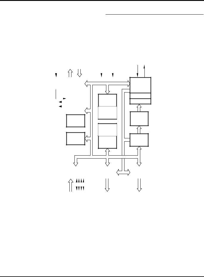
Counter/
Timers
Interrupt
Control
ALU
Flags |
Register |
Pointer |
Register File 208 x 8-Bytes
XTAL1 |
XTAL2 |
Machine
Timing & Inst.
Control
WDT
POR
Program
Memory
4 KB ROM
Program
Counter
Port 2 |
|
Port 0 |
|
Port 1 |
||||
|
|
|
|
|
|
|
|
|
4 |
|
|
|
I/O |
8 |
8 |
||
|
|
|
||||||
|
|
|
|
|||||
|
|
|
|
Open-Drain |
|
Open-Drain |
||
Input (Bit Programmable) |
|
|||||||
Output |
|
Output |
||||||
|
|
|
|
|
|
|
||
Figure 1. Z86KXX Functional Block Diagram
2 |
P R E L I M I N A R Y |
DS97KEY0204 |
|
Z86K13/K14/K15/K16/K17/K18 |
Zilog |
CMOS Z8® 8-Bit MCU Keyboard Controllers |
|
|
PIN DESCRIPTION
P30 |
|
1 |
40 |
|
|
P23 |
||
|
|
|||||||
P31 |
|
|
|
|
|
|
|
P22 |
|
|
|
|
|
|
|
||
P32 |
|
|
|
|
|
|
|
P21 |
|
|
|
|
|
|
|
||
P33 |
|
|
|
|
|
|
|
P20 |
|
|
|
|
|
|
|
||
*NC |
|
|
|
|
|
|
|
P37 |
|
|
|
|
|
|
|
||
*NC |
|
|
|
|
|
|
|
P36 |
|
|
|
|
|
|
|
||
P27 |
|
|
|
|
|
|
|
P35 |
|
|
|
|
|
|
|
||
P26 |
|
|
|
|
|
|
|
P34 |
|
|
|
|
|
|
|
||
P25 |
|
|
|
|
|
|
|
RCIN/XTAL1 |
|
|
|
|
|
|
|
||
P24 |
|
|
|
|
|
|
|
AGND/XTAL2 |
|
|
|
Z86KXX |
|
|
|||
GND |
|
|
|
DIP |
|
|
|
GND |
|
|
|
|
|
||||
VCC |
|
|
|
|
|
|
|
VCC |
|
|
|
|
|
|
|
||
P00 |
|
|
|
|
|
|
|
P17 |
|
|
|
|
|
|
|
||
P01 |
|
|
|
|
|
|
|
P16 |
|
|
|
|
|
|
|
||
P02 |
|
|
|
|
|
|
|
P15 |
|
|
|
|
|
|
|
||
P03 |
|
|
|
|
|
|
|
P14 |
|
|
|
|
|
|
|
||
P04 |
|
|
|
|
|
|
|
P13 |
|
|
|
|
|
|
|
||
P05 |
|
|
|
|
|
|
|
P12 |
|
|
|
|
|
|
|
||
P06 |
|
|
20 |
21 |
|
|
P11 |
|
|
|
|
|
|||||
P07 |
|
|
|
P10 |
||||
|
|
|||||||
|
|
|
|
|
|
|
|
|
Notes:
*Pin 5 and 6 used for testing Ground during normal operation. When Pin 5 is connected to VCC. Pin 6 is CLK OUT.
When Pin 5 is connected to GND, Pin 6 outputs nothing. These pins must be tied to ground in application.
Figure 2. 40-Pin DIP Configuration
Table 1. 40-Pin DIP Pin Identification
Pin # |
Symbol |
Function |
Direction |
|
|
|
|
1-4 |
P30-P33 |
Port 3, Pins 0,1,2,3 |
Input |
5-6 |
NC |
Tied to GND |
|
7-10 |
P27-P24 |
Port 2, Pins 7,6,5,4 |
In/Output |
11 |
GND |
Ground |
|
12 |
VCC |
Power Supply |
Input |
13-20 |
P00-P07 |
Port 0, Pins 0,1,2,3,4,5,6,7 |
Output |
21-28 |
P10-P17 |
Port 1, Pins 0,1,2,3,4,5,6,7 |
Output |
29 |
VCC |
Power Supply |
|
30 |
GND |
Ground |
|
31 |
AGND/XTAL2 |
Analog Ground or Crystal Clock Out |
|
32 |
RCIN/XTAL1 |
RCIN/Crystal Oscillator Clock |
Input |
33-36 |
P34-P37 |
Port 3, Pins 4,5,6,7 |
Output |
37-40 |
P20-P23 |
Port 2, Pins 0,1,2,3 |
Input |
|
|
|
|
DS97KEY0204 |
P R E L I M I N A R Y |
3 |
Z86K13/K14/K15/K16/K17/K18 |
|
CMOS Z8® 8-Bit MCU Keyboard Controllers |
Zilog |
PIN DESCRIPTION (Continued)
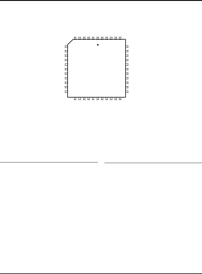
|
NC |
NC |
P33 |
P32 |
P31 |
P30 |
P23 |
P22 |
P21 |
P20 |
P37 |
|
||
|
6 |
|
|
|
|
|
1 |
|
|
|
|
|
40 |
|
NC |
7 |
|
|
|
|
|
|
|
|
|
|
|
39 |
NC |
P27 |
|
|
|
|
|
|
|
|
|
|
|
|
|
P36 |
P26 |
|
|
|
|
|
|
|
|
|
|
|
|
|
P35 |
P25 |
|
|
|
|
|
|
|
|
|
|
|
|
|
P34 |
P24 |
|
|
|
|
|
|
|
|
|
|
|
RCIN/XTAL1 |
||
|
|
|
|
|
Z86KXX |
|
|
|
|
|
||||
GND |
|
|
|
|
|
PLCC |
|
|
|
|
|
NC |
||
VCC |
|
|
|
|
|
|
|
|
|
|
|
|
|
AGND/XTAL2 |
|
|
|
|
|
|
|
|
|
|
|
|
|
||
P00 |
|
|
|
|
|
|
|
|
|
|
|
|
|
GND |
P01 |
|
|
|
|
|
|
|
|
|
|
|
|
|
VCC |
P02 |
|
|
|
|
|
|
|
|
|
|
|
|
|
P17 |
P03 |
17 |
|
|
|
|
|
|
|
|
|
|
|
29 |
NC |
|
18 |
|
|
|
|
|
|
|
|
|
|
|
28 |
|
|
P04 |
P05 |
P06 |
P07 |
P10 |
P11 |
P12 |
P13 |
P14 |
P15 |
P16 |
|
||
Notes:
Pins 5 and 6 used for testing. Ground during normal operation
When Pin 43 is connected to VCC, Pin 44 is CLKOUT.
When Pin 43 is connected to GND. Pin 44 outputs nothing.
Figure 3. 44-Pin PLCC Pin Assignments
Table 2. 44-Pin PLCC Pin Assignments
Pin # |
Symbol |
Function |
Direction |
|
|
|
|
1-4 |
P30-P33 |
Port 3, Pins |
Input |
|
|
0,1,2,3 |
|
|
|
|
|
5-7 |
NC |
Test Pins (GND) |
|
|
|
|
|
8-11 |
P27-P24 |
Port 2, Pins |
In/Output |
|
|
4,5,6,7 |
|
|
|
|
|
12 |
GND |
Ground |
|
|
|
|
|
13 |
VCC |
Power Supply |
|
14-21 |
P00-P07 |
Port 0, Pins |
Output |
|
|
0,1,2,3,4,5,6,7 |
|
|
|
|
|
22-28 |
P10-P16 |
Port 1, Pins |
Output |
|
|
0,1,2,3,4,5,6 |
|
|
|
|
|
29 |
NC |
Not Connected |
|
|
|
|
|
Table 2. 44-Pin PLCC Pin Assignments
Pin # |
Symbol |
Function |
Direction |
|
|
|
|
30 |
P17 |
Port 1, Pin 7 |
Output |
|
|
|
|
31 |
VCC |
Power Supply |
|
32 |
GND |
Ground |
|
|
|
|
|
33 |
AGND/ XTAL2 |
Analog Ground |
|
|
|
or Crystal Clock |
|
|
|
Out |
|
|
|
|
|
34 |
NC |
Not Connected |
|
|
|
|
|
35 |
RCIN/ XTAL1 |
RCIN/Crystal |
Input |
|
|
Oscillator Clock |
|
|
|
|
|
36-38 |
P34-P37 |
Port 3, Pins |
Output |
|
|
4,5,6,7 |
|
|
|
|
|
39 |
NC |
Not Connected |
|
|
|
|
|
40 |
P37 |
Port 3, Pin 7 |
Output |
|
|
|
|
41-44 |
P20-P23 |
Port 2, Pins |
In/Output |
|
|
0,1,2,3 |
|
|
|
|
|
4 |
P R E L I M I N A R Y |
DS97KEY0204 |
|
|
|
|
|
|
|
|
|
|
Z86K13/K14/K15/K16/K17/K18 |
Zilog |
|
|
|
|
|
|
|
|
CMOS Z8® 8-Bit MCU Keyboard Controllers |
|
|
|
|
|
|
|
|
|
|
|
|
|
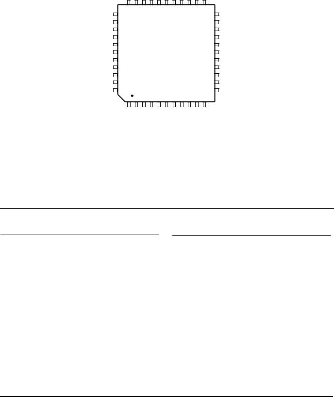
NC |
P36 |
P35 |
P34 |
RCIN/XTAL1 NC AGND/XTAL2 |
GND |
VCC |
P17 |
NC |
|
|
33 |
|
|
|
|
|
|
|
23 |
|
P37 |
34 |
|
|
|
|
|
|
|
22 |
P16 |
P20 |
|
|
|
|
|
|
|
|
|
P15 |
P21 |
|
|
|
|
|
|
|
|
|
P14 |
P22 |
|
|
|
|
|
|
|
|
|
P13 |
P23 |
|
|
|
|
Z86KXX |
|
|
|
|
P12 |
P30 |
|
|
|
|
|
|
|
|
P11 |
|
|
|
|
|
QFP |
|
|
|
|
||
P31 |
|
|
|
|
|
|
|
|
P10 |
|
|
|
|
|
|
|
|
|
|
||
P32 |
|
|
|
|
|
|
|
|
|
P07 |
P33 |
|
|
|
|
|
|
|
|
|
P06 |
NC |
|
|
|
|
|
|
|
|
|
P05 |
NC |
44 |
|
|
|
|
|
|
|
12 |
P04 |
|
1 |
|
|
|
|
|
|
|
11 |
|
|
NC |
P27 |
P26 |
P25 |
P24 GND VCC |
P00 |
P01 |
P02 |
P03 |
|
Notes:
Pins 43 and 44 are used for testing ground during normal operation.
When Pin 45 is connected to VCC, Pin 46 is CLKOUT.
When Pin 45 is connected to GND. Pin 46 outputs nothing.
Figure 4. 44-Pin QFP Pin Assignments
Table 3. 44-Pin QFP Pin Identification
Pin # |
Symbol |
Function |
Direction |
|
|
|
|
1 |
NC |
Not Connected |
|
|
|
|
|
2-5 |
P24-P27 |
Port 2, Pins |
In/Output |
|
|
4,5,6,7 |
|
|
|
|
|
6 |
GND |
Ground |
|
|
|
|
|
7 |
VCC |
Supply Voltage |
|
8-15 |
P00-P07 |
Port 0, Pins |
Output |
|
|
0,1,2,3,4,5,6,7, |
|
|
|
|
|
16-22 |
P10-P16 |
Port 1, Pins |
Output |
|
|
0,1,2,3,4,5,6 |
|
|
|
|
|
23 |
NC |
Not Connected |
|
|
|
|
|
24 |
P17 |
Port 1, Pin 7 |
Output |
|
|
|
|
25 |
VCC |
Supply Voltage |
|
Table 3. 44-Pin QFP Pin Identification
Pin # |
Symbol |
Function |
Direction |
|
|
|
|
26 |
GND |
Ground |
|
|
|
|
|
27 |
AGND/ XTAL2 Analog Ground/ |
|
|
|
|
Crystal Clock Out |
|
|
|
|
|
28 |
NC |
Not Connected |
|
|
|
|
|
29 |
RCIN / XTAL1 |
RCIN/Crystal |
Input |
|
|
Oscillator Clock |
|
|
|
|
|
30-32 |
P34-P36 |
Port 3, Pins 4,5,6 |
Output |
|
|
|
|
33 |
NC |
Not Connected |
|
|
|
|
|
34 |
P37 |
Port 3, Pin 7 |
Output |
|
|
|
|
35-38 |
P20-P23 |
Port 2, Pins |
Input |
|
|
0,1,2,3 |
|
|
|
|
|
39-42 |
P30-P33 |
Port 3, Pins |
Input |
|
|
0,1,2,3 |
|
|
|
|
|
43-44 |
NC |
Test Pins (GND) |
|
|
|
|
|
DS97KEY0204 |
P R E L I M I N A R Y |
5 |
Z86K13/K14/K15/K16/K17/K18 |
|
CMOS Z8® 8-Bit MCU Keyboard Controllers |
Zilog |
ABSOLUTE MAXIMUM RATINGS
Symbol |
Description |
Min |
Max |
Units |
|
|
|
|
|
VCC |
Supply Voltage* |
–0.3 |
+7.0 |
V |
TSTG |
Storage Temp |
–65 |
+150 |
°C |
TA |
Oper Ambient Temp |
0 |
+105 |
°C |
Note: * Voltage on all pins with respect to GND.
Stresses greater than those listed under Absolute Maximum Ratings may cause permanent damage to the device. This is a stress rating only; operation of the device at any condition above those indicated in the operational sections of these specifications is not implied. Exposure to absolute maximum rating conditions for extended periods may affect device reliability.
STANDARD TEST CONDITIONS
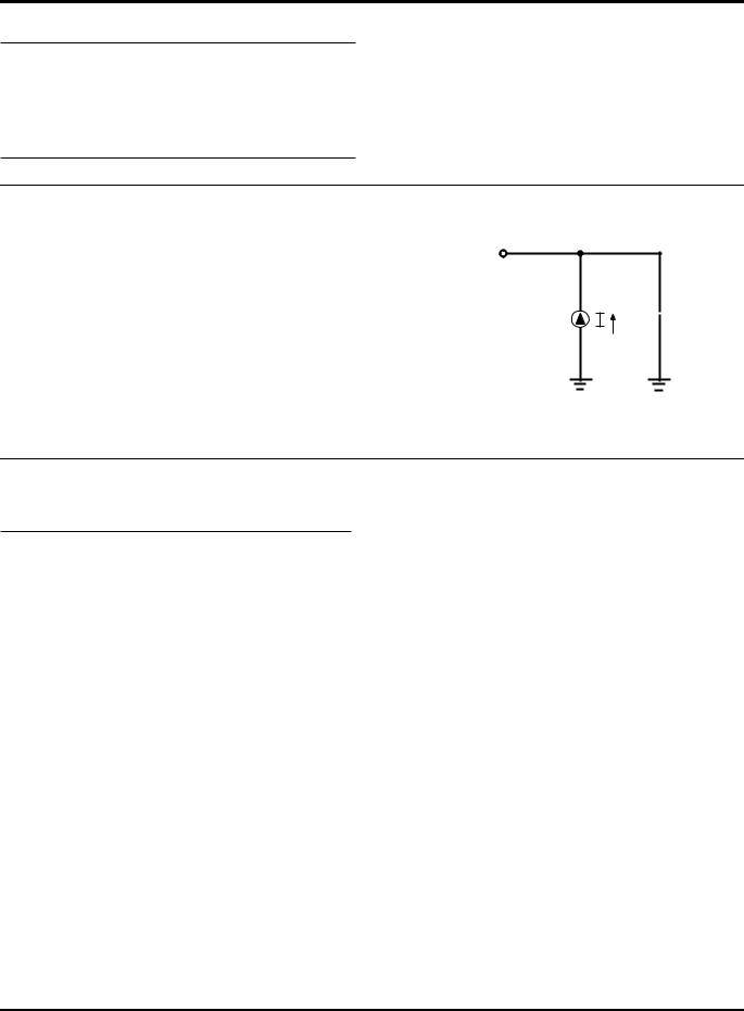
The characteristics listed here apply for standard test conditions as noted. All voltages are referenced to GND. Positive current flows into the referenced pin (Figure 5).
From Output
Under Test
 150 pF
Figure 5. Test Load Diagram
CAPACITANCE
TA = 25°C; VCC = GND = 0V; f = 1.0 MHz; unmeasured pins returned to GND.
Parameter |
Max |
|
|
Input Capacitance |
12 pF |
Output Capacitance |
12 pF |
I/O Capacitance |
12 pF |
|
|
Frequency tolerance ±10%
6 |
P R E L I M I N A R Y |
DS97KEY0204 |

|
Z86K13/K14/K15/K16/K17/K18 |
Zilog |
CMOS Z8® 8-Bit MCU Keyboard Controllers |
|
|
DC CHARACTERISTICS
VCC = 5.0V ± 10% @ 0°C to +70°C
Sym |
Parameter |
Min |
Max |
Typ* |
Unit |
Condition |
|
|
|
|
|
|
|
VCH |
Clock Input High Voltage |
0.7 VCC |
VCC + 0.3V |
2.5 |
V |
Driven by External Clock Generator |
VCL |
Clock Input Low Voltage |
GND –0.3 |
0.2 VCC |
1.5 |
V |
Driven by External Clock Generator |
VIH |
Input High Voltage |
0.7 VCC |
VCC + 0.3 |
2.5 |
V |
|
VIL |
Input Low Voltage |
GND –0.3 |
0.2 VCC |
1.5 |
V |
|
VOH |
Output High Voltage |
VCC –0.4 |
|
4.7 |
V IOH = –2.0 mA |
|
VOH |
Output High Voltage |
VCC –0.6 |
|
|
V IOH = –2.0 mA (see note 1 below.) |
|
VOL |
Output Low Voltage |
|
.4 |
|
V |
IOL= 4 mA |
VOL |
Output Low Voltage |
|
.8 |
|
V |
IOL= 4 mA (see note 1 below.) |
IOL |
Output Low |
10 |
20 |
|
mA |
VOL= VCC –2.2 V (see note 1, 2 below.) |
IOL |
Output Leakage |
–1 |
1 |
<1 |
A |
VIN = 0V, 5.25V |
ICC |
VCC Supply Current |
|
12 |
6 |
mA |
@ 5.0 MHz |
ICC1 |
Halt Mode Current |
|
|
2 |
mA |
@ 5.0 MHz |
ICC2 |
Stop Mode Current |
|
10 |
|
A |
|
Rp |
Pull Up Resistor |
6.76 |
14.04 |
10.4 |
K ohm |
|
|
|
|
|
|
|
|
Rp |
Pull Up Resistor (P26-P27) |
1.8 |
3 |
2.4 |
K ohm |
|
|
|
|
|
|
|
|
Notes:
*Typical @ 25°C
1.Ports P37-P34. These may be used for LEDs or as general-purpose outputs requiring high sink current.
2.Vcc = 5.0V ± 5% @ 0°C to + 70°C
DS97KEY0204 |
P R E L I M I N A R Y |
7 |

Z86K13/K14/K15/K16/K17/K18 |
|
CMOS Z8® 8-Bit MCU Keyboard Controllers |
Zilog |
AC ELECTRICAL CHARACTERISTICS
|
|
|
VCC |
TA = 0°C to 70°C |
|
|
|
No |
Symbol |
Parameter |
5 MHz |
Units |
Notes |
||
Note[4] |
Min |
Max |
|||||
|
|
|
|
|
|
|
|
1 |
TpC |
Input Clock Period |
5.0V |
200 |
250 |
ns |
1 |
|
|
|
|
|
|
|
|
2 |
TrC,TfC |
Clock Input Rise & Fall Times |
5.0V |
|
25 |
ns |
1 |
|
|
|
|
|
|
|
|
3 |
TwC |
Input Clock Width |
5.0V |
37 |
|
ns |
1 |
|
|
|
|
|
|
|
|
4 |
TwTinL |
Timer Input Low Width |
5.0V |
70 |
|
ns |
1 |
|
|
|
|
|
|
|
|
5 |
TwTinH |
Timer Input High Width |
5.0V |
2.5TpC |
|
|
1 |
|
|
|
|
|
|
|
|
6 |
TpTin |
Timer Input Period |
5.0V |
4TpC |
|
|
1 |
|
|
|
|
|
|
|
|
7 |
TrTin, |
Timer Input Rise & Fall Timer |
5.0V |
|
100 |
ns |
|
|
|
|
|
|
|
|
|
8A |
TwIL |
Int. Request Low Time |
5.0V |
70 |
|
ns |
1,2 |
|
|
|
|
|
|
|
|
8B |
TwIL |
Int. Request Low Time |
5.0V |
3TpC |
|
|
1,3 |
|
|
|
|
|
|
|
|
9 |
TwIH |
Int. Request Input High Time |
5.0V |
3TpC |
|
|
1,2 |
|
|
|
|
|
|
|
|
10 |
Twsm |
STOP Mode Recovery Width Spec |
5.0V |
5TpC |
|
ns |
|
|
|
|
|
|
|
|
|
11 |
Tost |
Oscillator Start-up Time |
5.0V |
|
5TpC |
|
|
|
|
|
|
|
|
|
|
12 |
Twdt |
Watch-Dog Timer Delay Time |
5.0V |
53 |
|
ms |
|
|
|
|
|
|
|
|
|
13 |
TPOR |
Power--On Reset |
5.0V |
106 |
130 |
ms |
|
Notes:
1.Timing Reference uses 0.7 VCC for a logic 1 and 0.2 VCC for a logic 0.
2.Interrupt request through Port 3 (P31-P33).
3.Interrupt request through Port 3 (P30).
1 |
3 |
Clock
2 |
2 |
3 |
7 |
7 |
TIN |
|
4 |
5 |
|
6 |
IRQN |
|
8 |
9 |
Clock
Setup
11
Stop
Mode
Recovery
Source
10
Figure 6. Additional Timing
8 |
P R E L I M I N A R Y |
DS97KEY0204 |
 Loading...