


ZILOG Z86L8708FSC, Z86L8708PSC, Z86L8708VSC, Z86L8808PSC, Z86L8808SSC Datasheet
...PRELIMINARY PRODUCT SPECIFICATION
1
Z86L88/81/86/87/89/73 1
IR/LOW-VOLTAGE MICROCONTROLLER
FEATURES
|
ROM |
RAM* |
I/O |
Voltage |
|
– |
Programmable Input Glitch Filter for Pulse |
|
Device |
(KB) |
(Bytes) |
Lines |
Range |
|
|
Reception |
|
|
|
|
|
|
|
|
|
|
Z86L88 |
16 |
237 |
23 |
2.0V to 3.9V |
■ |
Five Priority Interrupts |
||
Z86L81 |
24 |
237 |
23 |
2.0V to 3.9V |
||||
|
– |
Three External |
||||||
Z86L86 |
32 |
237 |
23 |
2.0V to 3.9V |
|
|||
|
– Two Assigned to Counter/Timers |
|||||||
Z86L87 |
16 |
236 |
31 |
2.0V to 3.9V |
|
|||
|
|
|
||||||
Z86L89 |
24 |
236 |
31 |
2.0V to 3.9V |
■ |
Low Voltage Detection and Standby Mode |
||
Z86L73 |
32 |
236 |
31 |
2.0V to 3.9V |
■ Programmable Watch-Dog/Power-On Reset Circuits |
|||
|
|
|
|
|
||||
|
|
|
|
|
||||
Note: *General-Purpose
■Low Power Consumption - 40 mW (Typical)
■Three Standby Modes
–STOP
–HALT
–Low Voltage
■Special Architecture to Automate Both Generation and Reception of Complex Pulses or Signals:
–One Programmable 8-Bit Counter/Timer with Two Capture Registers
–One Programmable 16-Bit Counter/Timer with One 16-Bit Capture Register
■Two Independent Comparators with Programmable Interrupt Polarity
■On-Chip Oscillator that Accepts a Crystal, Ceramic Resonator, LC, RC (Mask Option), or External Clock Drive
■Mask Selectable 200 kOhms Pull-Ups on Ports 0, 2, 3
–All Eight Port 2 Bits at One Time or Not
–Pull-Ups Automatically Disabled Upon Selecting Individual Pins as Outputs.
■Maskable Mouse/Trackball Interface on P00 Through P03.
■32 kHz Oscillator Mask Option
GENERAL DESCRIPTION
The Z86LXX family of IR (Infrared) CCP™ (Consumer Controller Processor) Controllers are ROM/ROMless-based members of the Z8® single-chip microcontroller family with 256 bytes of internal RAM. The differentiating factor between these devices is the availability of ROM, and package options. For the 40 and 44-pin devices the use of external memory enables these Z8 microcontrollers to be used where code flexibility is required. Zilog’s CMOS microcontrollers offers fast executing, efficient use of memory, sophisticated interrupts, input/output bit manipulation capabilities, automated pulse generation/reception, and in-
ternal key-scan pull-up resistors. The Z86LXX product line offers easy hardware/software system expansion cost-ef- fective and low power consumption.
The Z86LXX architecture is based on Zilog's 8-bit microcontroller core with an Expanded Register File to allow access to register mapped peripherals, I/O circuits, and powerful counter/timer circuitry. The CCP offers a flexible I/O scheme, an efficient register and address space structure, and a number of ancillary features that are useful in many
DS96LV00800 |
P R E L I M I N A R Y |
1 |
Z86L88/81/86/87/89/73
IR/Low-Voltage Microcontroller
GENERAL DESCRIPTION (Continued)
consumer, automotive, computer peripheral, and battery operated hand-held applications.
There are four basic address spaces available to support a wide range of configurations: Program Memory, Register File, Expanded Register File, and External Memory. The register file is composed of 256 bytes of RAM. It includes four I/O port registers, 16 control and status registers and the rest are General Purpose registers. The Expanded Register File consists of two additional register groups (F and D). External Memory is not available on 28pin versions.
To unburden the program from coping with such real-time problems as generating complex waveforms or receiving and demodulating complex waveform/pulses, the Z86LXX family offers a new intelligent counter/timer architecture
HI16
 8
8
with 8-bit and 16-bit counter/timers (Figure 1). Also included are a large number of user-selectable modes, and two on-board comparators to process analog signals with separate reference voltages (Figure 2).
Notes: All Signals with a preceding front slash, "/", are active Low, e.g., B//W (WORD is active Low); /B/W (BYTE is active Low, only).
Power connections follow conventional descriptions below:
Connection |
Circuit |
Device |
|
|
|
Power |
VCC |
VDD |
Ground |
GND |
VSS |
LO16
 8
8
|
|
|
|
16-Bit |
|
Timer 16 |
|
|
|
|
T16 |
|
|
|
|
|
|
|
|
|
1 |
2 |
4 |
8 |
16 |
|
|
|
|
|
8 |
|
8 |
|
SCLK |
Clock |
TC16H |
|
TC16L |
|
|
|
Divider |
|
|
|||
|
|
|
|
|
And/Or |
Timer 8/16 |
|
|
|
|
|
Logic |
|
|
|
|
|
|
|
|
|
|
|
HI8 |
|
LO8 |
|
|
|
|
8 |
|
8 |
|
Input Glitch |
|
Edge |
|
|
|
|
|
Detect |
|
|
|
||
Filter |
|
8-Bit |
|
Timer 8 |
||
|
Circuit |
|
||||
|
|
T8 |
|
|||
|
|
|
|
|
|
|
|
|
|
8 |
|
8 |
|
|
|
|
TC8H |
|
TC8L |
|
Figure 1. Counter/Timers Diagram
2 |
P R E L I M I N A R Y |
DS96LV00800 |
|
|
|
|
|
|
Z86L88/81/86/87/89/73 |
|
|
|
|
|
|
|
IR/Low-Voltage Microcontroller |
|
|
P00 |
|
Register File |
|
|
Pref1 |
|
|
P01 |
|
|
|
|||
|
|
|
|
P31 |
|||
|
4 |
|
256 x 8-bit |
|
|
||
|
P02 |
|
|
|
P32 |
||
|
|
|
|
|
|
||
|
P03 |
|
|
|
|
|
P33 |
|
P04 |
|
Port 0 |
|
|
Port 3 |
P34 |
|
|
Register Bus |
|
|
|
||
|
|
|
|
|
P35 |
||
|
P05 |
|
|
|
|
||
|
4 |
|
Internal |
|
|
||
|
|
|
|
P36 |
|||
|
|
|
|
|
|||
|
P06 |
|
|
Address Bus |
|
|
|
|
|
|
|
|
P37 |
||
|
P07 |
|
|
|
|
|
|
|
|
ROM |
|
|
|
|
|
|
|
|
|
|
Z8 Core |
|
|
|
|
|
24K/32K x 8 |
|
|
|
|
|
|
|
|
|
|
|
|
|
P10 |
|
|
Internal Data Bus |
|
|
|
|
P11 |
|
|
|
|
|
|
|
|
|
|
|
|
|
|
|
P12 |
|
|
|
|
|
|
|
P13 |
8 |
Port 1 |
|
|
Machine |
XTAL |
|
P14 |
|
|
|
|||
|
|
|
|
|
|
||
|
|
|
Expanded |
Timing |
|
||
|
P15 |
|
|
/AS |
|||
|
|
Expanded |
Register Bus |
& |
|||
|
P16 |
|
|||||
|
|
Register |
|
|
Instruction |
/DS |
|
|
P17 |
|
|
|
|||
|
|
File |
|
|
Control |
R/W |
|
|
|
|
|
|
|||
|
|
|
|
|
|
|
/RESET |
|
P20 |
|
|
|
|
|
R//RL |
|
P21 |
|
|
|
|
|
|
|
|
|
|
|
|
(44-Pin) |
|
|
P22 |
|
|
|
|
|
|
|
|
|
|
|
|
VDD |
|
|
P23 |
|
|
|
|
Power |
|
I/O Bit |
|
Port 2 |
|
|
VSS |
||
P24 |
|
|
|
|
|||
Programmable |
|
|
|
|
|
|
|
|
P25 |
|
Counter/Timer 8 |
Counter/Timer 16 |
|
||
|
P26 |
|
|
||||
|
P27 |
|
8-Bit |
|
16-Bit |
|
|
Figure 2. Functional Block Diagram
DS96LV00800 |
P R E L I M I N A R Y |
3 |
Z86L88/81/86/87/89/73
IR/Low-Voltage Microcontroller
PIN DESCRIPTION
P25 |
|
1 |
28 |
|
|
P24 |
||
|
|
|||||||
P26 |
|
|
|
|
|
|
|
P23 |
|
|
|
|
|
|
|
||
P27 |
|
|
|
|
|
|
|
P22 |
|
|
|
|
|
|
|
||
P04 |
|
|
|
|
|
|
|
P21 |
|
|
|
|
|
|
|
||
P05 |
|
|
|
|
|
|
|
P20 |
|
|
|
|
|
|
|
||
P06 |
|
|
|
|
|
|
|
P03 |
|
|
|
Z86L88/86/81 |
|
|
|
||
P07 |
|
|
|
|
|
|
VSS |
|
|
|
|
DIP |
|
|
|
||
VDD |
|
|
|
|
|
|
P02 |
|
XTAL2 |
|
|
|
|
|
|
|
P01 |
|
|
|
|
|
|
|
||
XTAL1 |
|
|
|
|
|
|
|
P00 |
|
|
|
|
|
|
|
||
P31 |
|
|
|
|
|
|
|
Pref1 |
|
|
|
|
|
|
|
||
P32 |
|
|
|
|
|
|
|
P36 |
|
|
|
|
|
|
|
||
P33 |
|
|
14 |
15 |
|
|
P37 |
|
|
|
|
|
|||||
P34 |
|
|
|
P35 |
||||
|
|
|||||||
|
|
|
|
|
|
|
|
|
Figure 3. 28-Pin DIP
Pin Assignments
P25 |
|
1 |
28 |
|
|
P24 |
||
|
|
|||||||
P26 |
|
|
|
|
|
|
|
P23 |
|
|
|
|
|
|
|
||
P27 |
|
|
|
|
|
|
|
P22 |
|
|
|
|
|
|
|
||
P04 |
|
|
|
|
|
|
|
P21 |
|
|
|
|
|
|
|
||
P05 |
|
|
|
|
|
|
|
P20 |
|
|
|
|
|
|
|
||
P06 |
|
|
|
|
|
|
|
P03 |
|
|
|
|
|
|
|
||
P07 |
|
|
|
Z86L88/86/81 |
|
|
|
VSS |
|
|
|
SOIC |
|
|
|
||
VDD |
|
|
|
|
|
|
P02 |
|
|
|
|
|
|
|
|
||
XTAL2 |
|
|
|
|
|
|
|
P01 |
|
|
|
|
|
|
|
||
XTAL1 |
|
|
|
|
|
|
|
P00 |
P31 |
|
|
|
|
|
|
|
Pref1 |
P32 |
|
|
|
|
|
|
|
P36 |
P33 |
|
|
|
|
|
|
|
P37 |
P34 |
|
14 |
15 |
|
|
P35 |
||
|
|
|
|
|
|
|
|
|
Figure 4. 28-Pin SOIC
Pin Assignments
4 |
P R E L I M I N A R Y |
DS96LV00800 |
Z86L88/81/86/87/89/73
IR/Low-Voltage Microcontroller
R//W |
|
1 |
40 |
|
|
/DS |
||
|
|
|||||||
P25 |
|
|
|
|
|
|
|
P24 |
|
|
|
|
|
|
|
||
P26 |
|
|
|
|
|
|
|
P23 |
|
|
|
|
|
|
|
||
P27 |
|
|
|
|
|
|
|
P22 |
|
|
|
|
|
|
|
||
P04 |
|
|
|
|
|
|
|
P21 |
|
|
|
|
|
|
|
||
P05 |
|
|
|
|
|
|
|
P20 |
|
|
|
|
|
|
|
||
P06 |
|
|
|
|
|
|
|
P03 |
|
|
|
|
|
|
|
||
P14 |
|
|
|
|
|
|
|
P13 |
|
|
|
|
|
|
|
||
P15 |
|
|
|
|
|
|
|
P12 |
|
|
|
|
|
|
|
||
P07 |
|
|
|
|
|
|
|
VSS |
|
|
|
Z86L73/89/87 |
|
|
|||
|
|
|
|
|
||||
VDD |
|
|
|
DIP |
|
|
|
P02 |
|
|
|
|
|
||||
P16 |
|
|
|
|
|
|
|
P11 |
|
|
|
|
|
|
|
||
P17 |
|
|
|
|
|
|
|
P10 |
|
|
|
|
|
|
|
||
XTAL2 |
|
|
|
|
|
|
|
P01 |
|
|
|
|
|
|
|
||
XTAL1 |
|
|
|
|
|
|
|
P00 |
|
|
|
|
|
|
|
||
P31 |
|
|
|
|
|
|
|
Pref1 |
|
|
|
|
|
|
|
||
P32 |
|
|
|
|
|
|
|
P36 |
|
|
|
|
|
|
|
||
P33 |
|
|
|
|
|
|
|
P37 |
|
|
|
|
|
|
|
||
P34 |
|
|
20 |
21 |
|
|
P35 |
|
|
|
|
|
|||||
/AS |
|
|
|
/RESET |
||||
|
|
|||||||
|
|
|
|
|
|
|
|
|
Figure 5. 40-Pin DIP
Pin Assignments
|
P20 |
P03 |
P13 |
P12 |
VSS |
VSS |
P02 |
P11 |
P10 |
P01 |
P00 |
|
|
6 |
|
|
|
|
1 |
|
|
|
|
40 |
|
P21 |
7 |
|
|
|
|
|
|
|
|
|
39 |
Pref1 |
P22 |
|
|
|
|
|
|
|
|
|
|
|
P36 |
P23 |
|
|
|
|
|
|
|
|
|
|
|
P37 |
P24 |
|
|
|
|
|
|
|
|
|
|
|
P35 |
/DS |
|
|
|
Z86L73/89/73 |
|
|
/RESET |
|||||
R//RL |
|
|
|
|
|
VSS |
||||||
R//W |
|
|
|
|
PLCC |
|
|
|
|
/AS |
||
P25 |
|
|
|
|
|
|
|
|
|
|
|
P34 |
P26 |
|
|
|
|
|
|
|
|
|
|
|
P33 |
P27 |
|
|
|
|
|
|
|
|
|
|
|
P32 |
P04 |
17 |
|
|
|
|
|
|
|
|
|
29 |
P31 |
|
18 |
|
|
|
|
|
|
|
|
|
28 |
|
|
P05 |
P06 |
P14 |
P15 |
P07 |
VDD |
VDD |
P16 |
P17 |
XTAL2 |
XTAL1 |
|
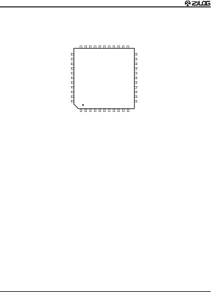
Figure 6. 44-Pin PLCC
Pin Assignments
DS96LV00800 |
P R E L I M I N A R Y |
5 |
Z86L88/81/86/87/89/73
IR/Low-Voltage Microcontroller
PIN DESCRIPTION (Continued)
|
P20 |
P03 |
P13 |
P12 |
VSS VSS P02 |
P11 |
P10 |
P01 |
P00 |
|
|
33 |
|
|
|
|
|
|
|
23 |
|
P21 |
34 |
|
|
|
|
|
|
|
22 |
Pref1 |
P22 |
|
|
|
|
|
|
|
|
|
P36 |
P23 |
|
|
|
|
|
|
|
|
|
P37 |
P24 |
|
|
|
|
|
|
|
|
|
P35 |
/DS |
|
|
|
|
|
|
|
|
|
/RESET |
R//RL |
|
|
|
|
|
|
|
|
|
VSS |
R//W |
|
|
|
Z86L73/89/87 |
|
|
|
/AS |
||
P25 |
|
|
|
|
QFP |
|
|
|
|
P34 |
P26 |
|
|
|
|
|
|
|
|
|
P33 |
P27 |
|
|
|
|
|
|
|
|
|
P32 |
P04 |
44 |
|
|
|
|
|
|
|
12 |
P31 |
|
1 |
|
|
|
|
|
|
|
11 |
|
|
P05 |
P06 |
P14 |
P15 |
P07 VDD VDD |
P16 |
P17 |
XTAL2 |
XTAL1 |
|
Figure 7. 44-Pin QFP
Pin Assignments
6 |
P R E L I M I N A R Y |
DS96LV00800 |

|
|
|
|
|
Z86L88/81/86/87/89/73 |
|
|
|
|
|
|
IR/Low-Voltage Microcontroller |
|
|
|
|
|
|
|
|
|
|
|
Table 1. Pin Identification |
|
|
|
|
|
|
|
|
|
|
40-Pin |
44-Pin |
44-Pin |
|
|
|
|
DIP # |
PLCC # |
QFP # |
Symbol |
Direction |
Description |
|
|
|
|
|
|
|
|
26 |
40 |
23 |
P00 |
Input/Output |
Port 0 is Nibble Programmable. |
|
|
|
|
|
|
|
|
27 |
41 |
24 |
P01 |
Input/Output |
Port 0 can be configured as |
|
|
|
|
|
|
|
|
30 |
44 |
27 |
P02 |
Input/Output |
A15-A8 external program |
|
|
|
|
|
|
|
|
34 |
5 |
32 |
P03 |
Input/Output |
ROM Address Bus. |
|
|
|
|
|
|
|
|
5 |
17 |
44 |
P04 |
Input/Output |
Port 0 can be configured as a |
|
|
|
|
|
|
|
|
6 |
18 |
1 |
P05 |
Input/Output |
mouse/trackball input. |
|
|
|
|
|
|
|
|
7 |
19 |
2 |
P06 |
Input/Output |
|
|
|
|
|
|
|
|
|
10 |
22 |
5 |
P07 |
Input/Output |
|
|
|
|
|
|
|
|
|
28 |
42 |
25 |
P10 |
Input/Output |
Port 1 is byte programmable. |
|
|
|
|
|
|
|
|
29 |
43 |
26 |
P11 |
Input/Output |
Port 1 can be configured as |
|
|
|
|
|
|
|
|
32 |
3 |
30 |
P12 |
Input/Output |
multiplexed A7-A0/D7-D0 |
|
|
|
|
|
|
|
|
33 |
4 |
31 |
P13 |
Input/Output |
external program ROM |
|
|
|
|
|
|
|
|
8 |
20 |
3 |
P14 |
Input/Output |
Address/Data Bus. |
|
|
|
|
|
|
|
|
9 |
21 |
4 |
P15 |
Input/Output |
|
|
|
|
|
|
|
|
|
12 |
25 |
8 |
P16 |
Input/Output |
|
|
|
|
|
|
|
|
|
13 |
26 |
9 |
P17 |
Input/Output |
|
|
|
|
|
|
|
|
|
35 |
6 |
33 |
P20 |
Input/Output |
Port 2 pins are individually |
|
|
|
|
|
|
|
|
36 |
7 |
34 |
P21 |
Input/Output |
configurable as input or output. |
|
|
|
|
|
|
|
|
37 |
8 |
35 |
P22 |
Input/Output |
|
|
|
|
|
|
|
|
|
38 |
9 |
36 |
P23 |
Input/Output |
|
|
|
|
|
|
|
|
|
39 |
10 |
37 |
P24 |
Input/Output |
|
|
|
|
|
|
|
|
|
2 |
14 |
41 |
P25 |
Input/Output |
|
|
|
|
|
|
|
|
|
3 |
15 |
42 |
P26 |
Input/Output |
|
|
|
|
|
|
|
|
|
4 |
16 |
43 |
P27 |
Input/Output |
|
|
|
|
|
|
|
|
|
16 |
29 |
12 |
P31 |
Input |
IRQ2/Modulator input |
|
|
|
|
|
|
|
|
17 |
30 |
13 |
P32 |
Input |
IRQ0 |
|
|
|
|
|
|
|
|
18 |
31 |
14 |
P33 |
Input |
IRQ1 |
|
|
|
|
|
|
|
|
19 |
32 |
15 |
P34 |
Output |
T8 output |
|
|
|
|
|
|
|
|
22 |
36 |
19 |
P35 |
Output |
T16 output |
|
|
|
|
|
|
|
|
24 |
38 |
21 |
P36 |
Output |
T8/T16 output |
|
|
|
|
|
|
|
|
23 |
37 |
20 |
P37 |
Output |
|
|
|
|
|
|
|
|
|
20 |
33 |
16 |
/AS |
Output |
Address Strobe |
|
|
|
|
|
|
|
|
40 |
11 |
38 |
/DS |
Output |
Data Strobe |
|
|
|
|
|
|
|
|
1 |
13 |
40 |
R//W |
Output |
Read/Write |
|
|
|
|
|
|
|
|
21 |
35 |
18 |
/RESET |
Input |
Reset |
|
|
|
|
|
|
|
|
15 |
28 |
11 |
XTAL1 |
Input |
Crystal, Oscillator Clock |
|
|
|
|
|
|
|
|
14 |
27 |
10 |
XTAL2 |
Output |
Crystal, Oscillator Clock |
|
|
|
|
|
|
|
|
11 |
23,24 |
6,7 |
VDD |
|
Power Supply |
|
31 |
1,2, 34 |
17,28,29 |
VSS |
|
Ground |
|
25 |
39 |
22 |
Pref1 |
Input |
Comparator 1 Reference |
|
|
|
|
|
|
|
|
|
12 |
39 |
R//RL |
Input |
ROM/ROMless |
|
|
|
|
|
|
|
|
DS96LV00800 |
P R E L I M I N A R Y |
7 |

Z86L88/81/86/87/89/73
IR/Low-Voltage Microcontroller
PIN DESCRIPTION (Continued)
Table 2. Pin Identification
28-Pin |
|
|
|
DIP & SOIC |
Symbol |
Direction |
Description |
|
|
|
|
19 |
P00 |
Input/Output |
Port 0 is Nibble Programmable |
|
|
|
|
20 |
P01 |
Input/Output |
Port 0 can be configured as |
|
|
|
|
21 |
P02 |
Input/Output |
A15-A8 external program |
|
|
|
|
23 |
P03 |
Input/Output |
ROM Address Bus. |
|
|
|
|
4 |
P04 |
Input/Output |
|
|
|
|
|
5 |
P05 |
Input/Output |
Port 0 can be configured as a |
|
|
|
mouse/trackball input. |
|
|
|
|
6 |
P06 |
Input/Output |
|
|
|
|
|
7 |
P07 |
Input/Output |
|
|
|
|
|
24 |
P20 |
Input/Output |
Port 2 pins are individually |
|
|
|
|
25 |
P21 |
Input/Output |
configurable as input or output. |
|
|
|
|
26 |
P22 |
Input/Output |
|
|
|
|
|
27 |
P23 |
Input/Output |
|
|
|
|
|
28 |
P24 |
Input/Output |
|
|
|
|
|
1 |
P25 |
Input/Output |
|
|
|
|
|
2 |
P26 |
Input/Output |
|
|
|
|
|
3 |
P27 |
Input/Output |
|
|
|
|
|
18 |
Pref1 |
Input |
Analog Ref Input |
|
|
|
|
11 |
P31 |
Input |
IRQ2/Modulator input |
|
|
|
|
12 |
P32 |
Input |
IRQ0 |
|
|
|
|
13 |
P33 |
Input |
IRQ1 |
|
|
|
|
14 |
P34 |
Output |
T8 output |
|
|
|
|
15 |
P35 |
Output |
T16 output |
|
|
|
|
17 |
P36 |
Output |
T8/T16 output |
|
|
|
|
16 |
P37 |
Output |
|
|
|
|
|
10 |
XTAL1 |
Input |
Crystal, Oscillator Clock |
|
|
|
|
9 |
XTAL2 |
Output |
Crystal, Oscillator Clock |
|
|
|
|
8 |
VDD |
|
Power Supply |
22 |
VSS |
|
Ground |
8 |
P R E L I M I N A R Y |
DS96LV00800 |
Z86L88/81/86/87/89/73
IR/Low-Voltage Microcontroller
ABSOLUTE MAXIMUM RATINGS
Symbol |
Description |
Min |
Max |
Units |
|
|
|
|
|
VCC |
Supply Voltage |
–0.3 |
+7.0 |
V |
|
(*) |
|
|
|
|
|
|
|
|
TSTG |
Storage Temp. |
–65° |
+150° |
C |
TA |
Oper. Ambient |
|
† |
C |
|
Temp. |
|
|
|
Notes: :
* Voltage on all pins with respect to GND.
† See Ordering Information.
Stresses greater than those listed under Absolute Maximum Ratings may cause permanent damage to the device. This is a stress rating only; operation of the device at any condition above those indicated in the operational sections of these specifications is not implied. Exposure to absolute maximum rating conditions for an extended period may affect device reliability.
STANDARD TEST CONDITIONS
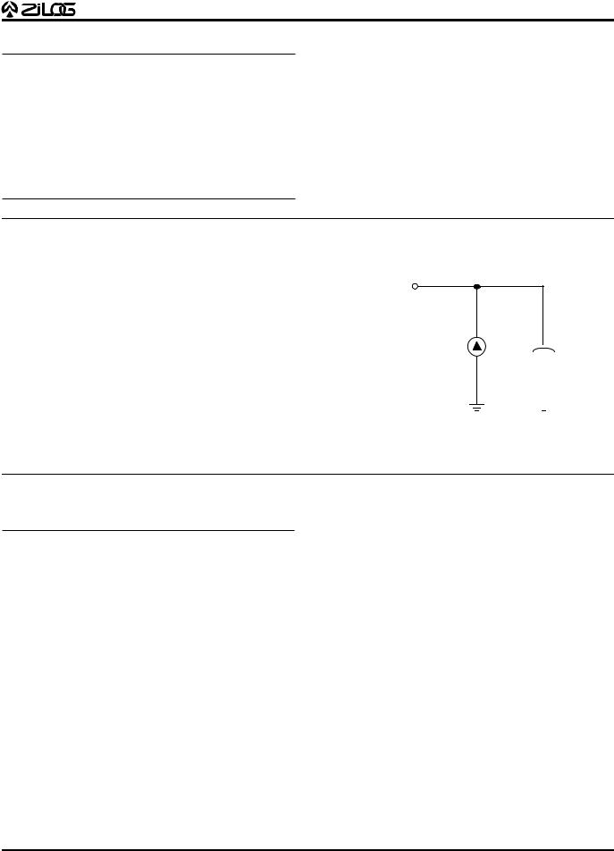
The characteristics listed below apply for standard test conditions as noted. All voltages are referenced to GND. Positive current flows into the referenced pin (Figure 8).
From Output
Under Test
I |
|
|
|
|
|
|
|
150 pF |
|
|
|
|
|
|
|
||
|
||||||||
|
|
|
|
|
|
|
|
|
|
|
|
|
|
|
|
|
|
Figure 8. Test Load Diagram
CAPACITANCE
TA = 25°C, VCC = GND = 0V, f = 1.0 MHz, unmeasured pins returned to GND.
Parameter |
Max |
|
|
Input capacitance |
12 pF |
|
|
Output capacitance |
12 pF |
|
|
I/O capacitance |
12 pF |
|
|
DS96LV00800 |
P R E L I M I N A R Y |
9 |

Z86L88/81/86/87/89/73
IR/Low-Voltage Microcontroller
DC CHARACTERISTICS
Preliminary
|
|
|
TA = 0°C to +70°C |
Typ @ |
|
|
|
|
|
Sym |
Parameter |
VCC |
Min |
Max |
25°C |
Units |
Conditions |
Notes |
|
|
Max Input Voltage 2.0V |
|
7 |
|
V |
IIN <250 A |
|
|
|
|
|
3.9V |
|
7 |
|
V |
IIN <250 A |
|
|
VCH |
Clock Input |
2.0V |
0.8 VCC |
VCC + 0.3 |
|
V |
Driven by External |
|
|
|
High Voltage |
|
|
|
|
|
Clock Generator |
|
|
|
|
3.9V |
0.8 VCC |
VCC + 0.3 |
|
V |
Driven by External |
|
|
|
|
|
|
|
|
|
Clock Generator |
|
|
VCL |
Clock Input |
2.0V |
VSS – 0.3 |
0.2 VCC |
|
V |
Driven by External |
|
|
|
Low Voltage |
|
|
|
|
|
Clock Generator |
|
|
|
|
3.9V |
VSS– 0.3 |
0.2 VCC |
|
V |
Driven by External |
|
|
|
|
|
|
|
|
|
Clock Generator |
|
|
VIH |
Input High Voltage2.0V |
0.7 VCC |
VCC + 0.3 |
0.5VCC |
V |
|
|
|
|
|
|
3.9V |
0.7 VCC |
VCC + 0.3 |
0.5VCC |
V |
|
|
|
VIL |
Input Low Voltage 2.0V |
VSS – 0.3 |
0.2 VCC |
0.5VCC |
V |
|
|
|
|
|
|
3.9V |
VSS – 0.3 |
0.2 VCC |
0.5VCC |
V |
|
|
|
VOH1 |
Output High |
2.0V |
VCC – 0.4 |
|
1.7 |
V IOH = –0.5 mA |
|
|
|
|
Voltage |
3.9V |
VCC – 0.4 |
|
3.7 |
V |
IOH = –0.5 mA |
|
|
VOH2 |
Output High |
2.0V |
VCC - 0.8 |
|
|
V IOH = –7 mA |
|
|
|
|
Voltage (P36, |
3.9V |
VCC - 0.8 |
|
|
V |
IOH = –7 mA |
|
|
|
P37,P00, P01) |
|
|
|
|
|
|
|
|
VOL1 |
Output Low |
2.0V |
|
0.4 |
0.1 |
V |
IOL = 1.0 mA |
|
|
|
Voltage |
3.9V |
|
0.4 |
0.2 |
V |
IOL = 4.0 mA |
|
|
VOL2* |
Output Low |
2.0V |
|
0.8 |
0.5 |
V IOL = 5.0 mA |
|
|
|
|
Voltage |
|
|
|
|
|
|
|
|
|
|
3.9V |
|
0.8 |
0.3 |
V |
IOL = 7.0 mA |
|
|
|
|
|
|
|
|
|
|
|
|
VOL2 |
Output Low |
2.0V |
|
0.8 |
0.3 |
V IOL = 10 mA |
|
|
|
|
Voltage(P36, |
3.9V |
|
0.8 |
0.2 |
V |
IOL = 10 mA |
|
|
|
P37,P00,P01) |
|
|
|
|
|
|
|
|
|
|
|
|
|
|
|
|
|
|
VRH |
Reset Input |
2.0V |
0.8 VCC |
VCC |
1.5 |
V |
|
|
|
|
High Voltage |
3.9V |
0.8 VCC |
VCC |
2.0 |
V |
|
|
|
VRl |
Reset Input |
2.0V |
VSS – 0.3 |
0.2 VCC |
0.5 |
V |
|
|
|
|
Low Voltage |
3.9V |
VSS – 0.3 |
0.2 VCC |
0.9 |
V |
|
|
|
VOFFSET |
Comparator Input 2.0V |
|
25 |
10 |
mV |
|
|
|
|
|
Offset Voltage |
3.9V |
|
25 |
10 |
mV |
|
|
|
IIL |
Input Leakage |
2.0V |
-1 |
1 |
< 1 |
A |
VIN = OV, VCC |
|
|
|
|
3.9V |
-1 |
1 |
< 1 |
A |
VIN = OV, VCC |
|
|
IOL |
Output Leakage |
2.0V |
–1 |
1 |
< 1 |
A |
VIN = OV, VCC |
|
|
|
|
3.9V |
–1 |
1 |
< 1 |
A |
VIN = OV, VCC |
|
|
IIR |
Reset Input Pull- |
2.0V |
|
–230 |
-90 |
A |
VIN = OV |
|
|
|
Up Current |
3.9V |
|
–400 |
–220 |
A |
VIN = OV‘ |
|
|
ICC |
Supply Current |
2.0V |
|
10 |
4 |
mA |
@ 8.0 MHz |
1,2 |
|
|
|
3.9V |
|
15 |
10 |
mA |
@ 8.0 MHz |
1,2 |
|
|
|
|
|
|
|
|
|
|
|
|
|
2.0V |
|
250 |
100 |
A |
@ 32 kHz |
1,2,7 |
|
|
|
3.9V |
|
850 |
500 |
A |
@ 32 kHz |
1,2,7 |
|
|
|
|
|
|
|
|
|
||
|
|
|
|
|
|
|
|
|
|
10 |
|
|
P R E L I M I N A R Y |
|
|
DS96LV00800 |
|||
Z86L88/81/86/87/89/73
IR/Low-Voltage Microcontroller
|
|
|
TA = 0°C to +70°C |
Typ @ |
|
|
|
|
Sym |
Parameter |
VCC |
Min |
Max |
25°C |
Units |
Conditions |
Notes |
ICC1 |
Standby Current |
2.0V |
|
3 |
1 |
mA |
HALT Mode |
1,2 |
|
(WDT Off) |
|
|
|
|
|
VIN = OV, VCC @ |
|
|
|
3.9V |
|
5 |
4 |
mA |
8.0 MHz |
1,2 |
|
|
|
HALT Mode |
|||||
|
|
|
|
|
|
|
VIN = OV, VCC |
|
|
|
|
|
|
|
|
@ 8.0 MHz |
|
|
|
|
|
|
|
|
|
|
|
|
2.0V |
|
2 |
0.8 |
mA |
Clock Divide-by- |
1,2 |
|
|
|
|
|
|
|
16 @ 8.0 MHz |
|
|
|
3.9V |
|
4 |
2.5 |
mA |
Clock Divide-by- |
1,2 |
|
|
|
|
|
|
|
16 @ 8.0 MHz |
|
|
|
|
|
|
|
|
|
|
ICC2 |
Standby Current |
2.0V |
|
8 |
2 |
A |
STOP Mode |
3,5 |
|
|
|
|
|
|
|
VIN = OV, VCC |
|
|
|
|
|
|
|
|
WDT is not |
|
|
|
3.9V |
|
10 |
3 |
A |
Running |
3,5 |
|
|
|
STOP Mode |
|||||
|
|
|
|
|
|
|
VIN = OV, VCC |
|
|
|
|
|
|
|
|
WDT is not |
|
|
|
|
|
|
|
|
Running |
|
|
|
|
|
|
|
|
|
|
|
|
2.0V |
|
500 |
310 |
A |
STOP Mode |
3,5 |
|
|
3.9V |
|
800 |
600 |
A |
VIN = OV, VCC |
|
|
|
|
|
|
|
|
WDT is Running |
|
|
|
|
|
|
|
|
|
|
TPOR |
Power-On Reset |
2.0V |
12 |
75 |
18 |
ms |
|
|
|
|
3.9V |
5 |
20 |
7 |
ms |
|
|
|
|
|
|
|
|
|
|
|
Vram |
Static RAM Data |
Vram |
0.8 |
|
0.5 |
V |
|
6 |
|
Retention Voltage |
|
|
|
|
|
|
|
|
|
|
|
|
|
|
|
|
VLV |
VCC Low Voltage |
|
|
2.15 |
1.7 |
V |
8 MHz max |
4 |
(Vbo) |
Protection |
|
|
|
|
|
Ext. CLK Freq. |
|
|
|
|
|
|
|
|
|
|
Notes: |
ICC1 |
Typ |
Max |
Unit |
Frequency |
|
|
|
|
Crystal/Resonator |
3.0 mA |
5 |
mA |
8.0 MHz |
|
|
|
|
External Clock Drive |
0.3 mA |
5 |
mA |
8.0 MHz |
|
|
|
1.All outputs unloaded, inputs at rail.
2.CL1 = CL2 = 100 pF
3.Same as note [4] except inputs at VCC.
4.The VLV increases as the temperature decreases.
5.Oscillator stopped.
6.Oscillator stops when VCC falls below Vlv limit
7.32 kHz clock driver input.
*All Outputs excluding P00, P01, P36, and P37.
DS96LV00800 |
P R E L I M I N A R Y |
11 |

Z86L88/81/86/87/89/73
IR/Low-Voltage Microcontroller
AC CHARACTERISTICS
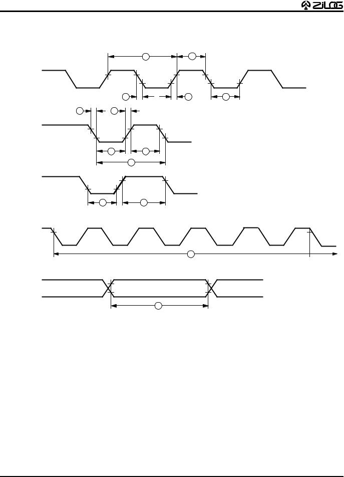
External I/O or Memory Read and Write Timing Diagram
R//W |
|
|
|
|
|
|
|
|
13 |
12 |
|
|
|
19 |
|
|
|
|
|
Port 0, /DM |
|
|
|
|
|
16 |
|
|
20 |
18 |
3 |
|
|
|
Port 1 |
A7 - A0 |
|
D7 - D0 |
IN |
|
|
|||
1 |
2 |
|
|
9 |
/AS |
|
|
|
|
|
|
8 |
|
11 |
4 |
|
|
|
|
|
5 |
6 |
|
|
/DS |
|
|
|
|
(Read) |
17 |
|
|
|
|
|
|
|
10 |
Port 1 |
A7 - A0 |
D7 - D0 |
OUT |
|
|
|
|||
|
14 |
|
|
15 |
|
|
|
7 |
|
/DS |
|
|
|
|
(Write) |
|
|
|
|
Figure 9. External I/O or Memory Read/Write Timing
12 |
P R E L I M I N A R Y |
DS96LV00800 |

Z86L88/81/86/87/89/73
IR/Low-Voltage Microcontroller
AC CHARACTERISTICS
Preliminary
External I/O or Memory Read and Write Timing Table
|
|
|
|
TA = 0°C to +70°C |
|
|
|
|
|
|
|
8.0MHz |
|
|
|
No |
Symbol |
Parameter |
VCC |
Min |
Max |
Units |
Notes |
1 |
TdA(AS) |
Address Valid to |
2.0V |
55 |
|
ns |
2 |
|
|
/AS Rising Delay |
3.9V |
55 |
|
ns |
|
|
|
|
|
|
|
|
|
2 |
TdAS(A) |
/AS Rising to Address |
2.0V |
70 |
|
ns |
2 |
|
|
Float Delay |
3.9V |
70 |
|
ns |
2 |
|
|
|
|
|
|
|
|
3 |
TdAS(DR) |
/AS Rising to Read |
2.0V |
|
400 |
ns |
1,2 |
|
|
Data Required Valid |
3.9V |
|
400 |
ns |
|
|
|
|
|
|
|
|
|
4 |
TwAS |
/AS Low Width |
2.0V |
80 |
|
ns |
2 |
|
|
|
3.9V |
80 |
|
ns |
|
|
|
|
|
|
|
|
|
5 |
Td |
Address Float to |
2.0V |
0 |
|
ns |
|
|
|
/DS Falling |
3.9V |
0 |
|
ns |
|
|
|
|
|
|
|
|
|
6 |
TwDSR |
/DS (Read) Low Width |
2.0V |
300 |
|
ns |
1,2 |
|
|
|
3.9V |
300 |
|
ns |
|
|
|
|
|
|
|
|
|
7 |
TwDSW |
/DS (Write) Low Width |
2.0V |
165 |
|
ns |
1,2 |
|
|
|
3.9V |
165 |
|
ns |
|
|
|
|
|
|
|
|
|
8 |
TdDSR(DR) |
/DS Falling to Read |
2.0V |
|
260 |
ns |
1,2 |
|
|
Data Required Valid |
3.9V |
|
260 |
ns |
|
|
|
|
|
|
|
|
|
9 |
ThDR(DS) |
Read Data to /DS Rising |
2.0V |
0 |
|
ns |
2 |
|
|
Hold Time |
3.9V |
0 |
|
ns |
|
|
|
|
|
|
|
|
|
10 |
TdDS(A) |
/DS Rising to Address |
2.0V |
85 |
|
ns |
2 |
|
|
Active Delay |
3.9V |
95 |
|
ns |
|
|
|
|
|
|
|
|
|
11 |
TdDS(AS) |
/DS Rising to /AS |
2.0V |
60 |
|
ns |
2 |
|
|
Falling Delay |
3.9V |
70 |
|
ns |
|
|
|
|
|
|
|
|
|
12 |
TdR/W(AS) |
R//W Valid to /AS |
2.0V |
70 |
|
ns |
2 |
|
|
Rising Delay |
3.9V |
70 |
|
ns |
|
|
|
|
|
|
|
|
|
13 |
TdDS(R/W) |
/DS Rising to |
2.0V |
70 |
|
ns |
2 |
|
|
R//W Not Valid |
3.9V |
70 |
|
ns |
|
|
|
|
|
|
|
|
|
14 |
TdDW(DSW) |
Write Data Valid to /DS |
2.0V |
80 |
|
ns |
2 |
|
|
Falling (Write) Delay |
3.9V |
80 |
|
ns |
|
|
|
|
|
|
|
|
|
15 |
TdDS(DW) |
/DS Rising to Write |
2.0V |
70 |
|
ns |
2 |
|
|
Data Not Valid Delay |
3.9V |
80 |
|
ns |
|
|
|
|
|
|
|
|
|
16 |
TdA(DR) |
Address Valid to Read |
2.0V |
|
475 |
ns |
1,2 |
|
|
Data Required Valid |
3.9V |
|
475 |
ns |
|
|
|
|
|
|
|
|
|
17 |
TdAS(DS) |
/AS Rising to |
2.0V |
100 |
|
ns |
2 |
|
|
/DS Falling Delay |
3.9V |
100 |
|
ns |
|
|
|
|
|
|
|
|
|
18 |
TdDM(AS) |
/DM Valid to /AS |
2.0V |
55 |
|
ns |
2 |
|
|
Falling Delay |
3.9V |
55 |
|
ns |
|
|
|
|
|
|
|
|
|
19 |
TdDS(DM) |
/DS Rise to |
2.0V |
70 |
|
ns |
|
|
|
/DM Valid Delay |
3.9V |
70 |
|
ns |
|
|
|
|
|
|
|
|
|
20 |
ThDS(A) |
/DS Rise to Address |
2.0V |
70 |
|
ns |
|
|
|
Valid Hold Time |
3.9V |
70 |
|
|
|
|
|
|
|
|
|
|
|
Notes:
1.When using extended memory timing add 2 TpC.
2.Timing numbers given are for minimum TpC.
Standard Test Load
All timing references use 0.9 VCC for a logic 1 and 0.1 VCC for a logic 0.
DS96LV00800 |
P R E L I M I N A R Y |
13 |
Z86L88/81/86/87/89/73
IR/Low-Voltage Microcontroller
AC CHARACTERISTICS
Additional Timing Diagram
1 |
3 |
Clock
2 |
2 |
3 |
7 |
7 |
TIN
4 |
5 |
6
IRQ N
8 |
9 |
Clock
Setup
11
Stop
Mode
Recovery
Source
10
Figure 10. Additional Timing
14 |
P R E L I M I N A R Y |
DS96LV00800 |

Z86L88/81/86/87/89/73
IR/Low-Voltage Microcontroller
AC CHARACTERISTICS
Preliminary
Additional Timing Table
|
|
|
|
|
|
|
|
|
|
|
|
TA = 0°C to +70°C |
|
|
|
|
|
|
|
8.0MHz |
|
|
|
No |
Sym |
Parameter |
VCC |
Min |
Max |
Units |
Notes |
1 |
TpC |
Input Clock Period |
2.0V |
121 |
DC |
ns |
1 |
|
|
|
3.9V |
121 |
DC |
ns |
1 |
|
|
|
|
|
|
|
|
2 |
TrC,TfC |
Clock Input Rise |
2.0V |
|
25 |
ns |
1 |
|
|
and Fall Times |
3.9V |
|
25 |
ns |
1 |
|
|
|
|
|
|
|
|
3 |
TwC |
Input Clock Width |
2.0V |
37 |
|
ns |
1 |
|
|
|
3.9V |
37 |
|
ns |
1 |
|
|
|
|
|
|
|
|
4 |
TwTinL |
Timer Input |
2.0V |
100 |
|
ns |
1 |
|
|
Low Width |
3.9V |
70 |
|
ns |
1 |
|
|
|
|
|
|
|
|
5 |
TwTinH |
Timer Input |
2.0V |
3TpC |
|
|
1 |
|
|
High Width |
3.9V |
3TpC |
|
|
1 |
|
|
|
|
|
|
|
|
6 |
TpTin |
Timer Input |
2.0V |
8TpC |
|
|
1 |
|
|
Period |
3.9V |
8TpC |
|
|
1 |
|
|
|
|
|
|
|
|
7 |
TrTin,TfTin |
Timer Input Rise |
2.0V |
|
100 |
ns |
1 |
|
|
and Fall Timers |
3.9V |
|
100 |
ns |
1 |
|
|
|
|
|
|
|
|
8A |
TwIL |
Interrupt Request |
2.0V |
100 |
|
ns |
1,2 |
|
|
Low Time |
3.9V |
70 |
|
ns |
1,2 |
|
|
|
|
|
|
|
|
8B |
TwIL |
Interrupt Request |
2.0V |
5TpC |
|
|
1,3 |
|
|
Low Time |
3.9V |
5TpC |
|
|
1,3 |
|
|
|
|
|
|
|
|
9 |
TwIH |
Interrupt Request |
2.0V |
5TpC |
|
|
1,2 |
|
|
Input High Time |
3.9V |
5TpC |
|
|
1,2 |
|
|
|
|
|
|
|
|
10 |
Twsm |
Stop-Mode Recovery |
2.0V |
12 |
|
ns |
7 |
|
|
Width Spec |
3.9V |
12 |
|
ns |
7 |
|
|
|
2.0V |
5 TpC |
|
ns |
6 |
|
|
|
3.9V |
5 TpC |
|
ns |
6 |
|
|
|
|
|
|
|
|
11 |
Tost |
Oscillator |
2.0V |
|
5TpC |
|
4 |
|
|
Start-Up Time |
3.9V |
|
5TpC |
|
4 |
|
|
|
|
|
|
|
|
12 |
Twdt |
Watch-Dog Timer |
2.0V |
12 |
75 |
ms |
|
|
|
Delay Time (5 ms) |
3.9V |
5 |
20 |
ms |
|
|
|
(10 ms) |
2.0V |
25 |
150 |
ms |
|
|
|
|
3.9V |
10 |
40 |
ms |
|
|
|
(20 ms) |
2.0V |
50 |
300 |
ms |
|
|
|
|
3.9V |
20 |
80 |
ms |
|
|
|
(80 ms) |
2.0V |
225 |
1200 |
ms |
|
|
|
|
3.9V |
80 |
320 |
ms |
|
|
|
|
|
|
|
|
|
Notes:
1.Timing Reference uses 0.9 VCC for a logic 1 and 0.1 VCC for a logic 0.
2.Interrupt request through Port 3 (P33-P31).
3.Interrupt request through Port 3 (P30).
4.SMR – D5 = 0
DS96LV00800 |
P R E L I M I N A R Y |
15 |
Z86L88/81/86/87/89/73
IR/Low-Voltage Microcontroller
AC CHARACTERISTICS
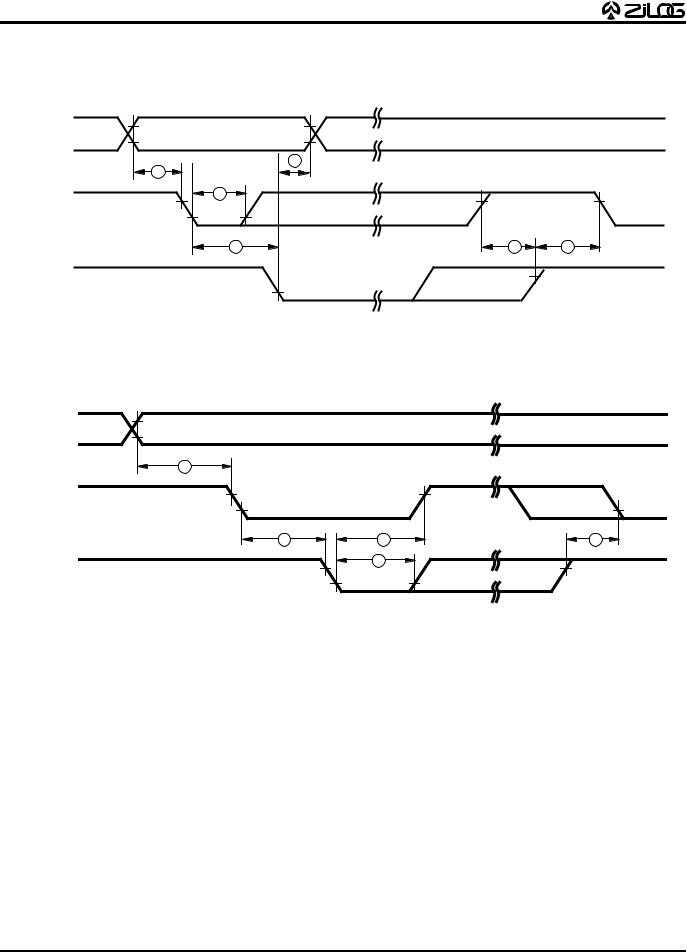
Handshake Timing Diagrams
Data In |
Data In Valid |
Next Data In Valid |
|
|
|
2 |
|
|
1 |
|
|
|
3 |
|
|
/DAV |
|
Delayed DAV |
|
(Input) |
|
|
|
|
4 |
5 |
6 |
RDY |
|
Delayed RDY |
|
(Output) |
|
|
|
Figure 11. Port Input Handshake Timing
Data Out |
Data Out Valid |
|
Next Data Out Valid |
|
7 |
|
|
/DAV |
|
|
Delayed DAV |
(Output) |
|
|
|
|
8 |
9 |
11 |
|
|
10 |
|
RDY |
|
|
Delayed RDY |
(Input) |
|
|
|
Figure 12. Port Output Handshake Timing
16 |
P R E L I M I N A R Y |
DS96LV00800 |

Z86L88/81/86/87/89/73
IR/Low-Voltage Microcontroller
AC CHARACTERISTICS
Preliminary
Handshake Timing Table
|
|
|
|
TA = 0°C to +70°C |
Data |
|
No |
Sym |
Parameter |
VCC |
Min |
Max |
Direction |
1 |
TsDI(DAV) |
Data In Setup Time |
2.0V |
0 |
|
IN |
|
|
|
3.9V |
0 |
|
IN |
|
|
|
|
|
|
|
2 |
ThDI(DAV) |
Data In Hold Time |
2.0V |
0 |
|
IN |
|
|
|
3.9V |
0 |
|
IN |
|
|
|
|
|
|
|
3 |
TwDAV |
Data Available Width |
2.0V |
155 |
|
IN |
|
|
|
3.9V |
110 |
|
IN |
|
|
|
|
|
|
|
4 |
TdDAVI(RDY) |
DAV Falling to RDY |
2.0V |
|
160 |
IN |
|
|
Falling Delay |
3.9V |
|
115 |
IN |
|
|
|
|
|
|
|
5 |
TdDAVId(RDY) |
DAV Rising to RDY |
2.0V |
|
120 |
IN |
|
|
Falling Delay |
3.9V |
|
80 |
IN |
|
|
|
|
|
|
|
6 |
TdRDYO(DAV) |
RDY Rising to DAV |
2.0V |
0 |
|
IN |
|
|
Falling Delay |
3.9V |
0 |
|
IN |
|
|
|
|
|
|
|
7 |
TdDO(DAV) |
Data Out to DAV |
2.0V |
63 |
|
OUT |
|
|
Falling Delay |
3.9V |
63 |
|
OUT |
|
|
|
|
|
|
|
8 |
TdDAV0(RDY) |
DAV Falling to RDY |
2.0V |
0 |
|
OUT |
|
|
Falling Delay |
3.9V |
0 |
|
OUT |
|
|
|
|
|
|
|
9 |
TdRDY0(DAV) |
RDY Falling to DAV |
2.0V |
|
160 |
OUT |
|
|
Rising Delay |
3.9V |
|
115 |
OUT |
|
|
|
|
|
|
|
10 |
TwRDY |
RDY Width |
2.0V |
110 |
|
OUT |
|
|
|
3.9V |
80 |
|
OUT |
|
|
|
|
|
|
|
11 |
TdRDY0d(DAV) |
RDY Rising to DAV |
2.0V |
|
110 |
OUT |
|
|
Falling Delay |
3.9V |
|
80 |
OUT |
|
|
|
|
|
|
|
DS96LV00800 |
P R E L I M I N A R Y |
17 |

Z86L88/81/86/87/89/73
IR/Low-Voltage Microcontroller
PIN FUNCTIONS
/DS (Output, active Low). Data Strobe is activated once for each external memory transfer. For a READ operation, data must be available prior to the trailing edge of /DS. For WRITE operations, the falling edge of /DS indicates that output data is valid.
/AS (Output, active Low). Address Strobe is pulsed once at the beginning of each machine cycle. Address output is through Port 0/Port 1 for all external programs. Memory address transfers are valid at the trailing edge of /AS. Under program control, /AS is placed in the high-impedance state along with Ports 0 and 1, Data Strobe, and Read/Write.
XTAL1 Crystal 1 (time-based input). This pin connects a parallel-resonant crystal, ceramic resonator, LC, or RC network or an external single-phase clock to the on-chip oscillator input.
XTAL2 Crystal 2 (time-based output). This pin connects a parallel-resonant, crystal, ceramic resonant, LC, or RC network to the on-chip oscillator output.
R//W Read/Write (output, write Low). The R//W signal is Low when the CCP is writing to the external program or data memory.
R//RL (input). This pin, when connected to GND, disables the internal ROM and forces the device to function as a ROMless Z8. (Note that, when left unconnected or pulled high to VCC, the part functions normally as a Z8 ROM version.)
Port 0 (P07-P00). Port 0 is an 8-bit, bidirectional, CMOS compatible port. These eight I/O lines are configured under software control as a nibble I/O port, or as an address port for interfacing external memory. The output drivers are push-pull. Port 0 can be placed under handshake control. In this configuration, Port 3, lines P32 and P35 are used as the handshake control /DAV0 and RDY0. Handshake signal function is dictated by the I/O direction of the Port 0 upper nibble P07-P04. The lower nibble must have the same direction as the upper nibble.
For external memory references, Port 0 can provide address bits A11-A8 (lower nibble) or A15-A8 (lower and upper nibble) depending on the required address space. If the address range requires 12 bits or less, the upper nibble of Port 0 can be programmed independently as I/O while the lower nibble is used for addressing. If one or both nibbles are needed for I/O operation, they must be configured by writing to the Port 0 mode register. After a hardware reset, Port 0 is configured as an input port.
Port 0 is set in the high-impedance mode (if selected as an address output) along with Port 1 and the control signals /AS, /DS, and R//W through P3M bits D4 and D3(Figure 13).
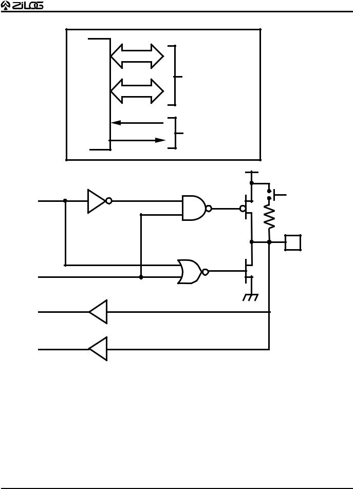
A ROM mask option is available to program 0.4 VDD CMOS trip inputs on P00-P03. This allows direct interface to mouse/trackball IR sensors.
An optional 200 kOhms pull-up is available as a mask option on all Port 0 bits with nibble select.
Note: Internal pull-ups are disabled on any given pin or group of port pins when programmed into output mode.
18 |
P R E L I M I N A R Y |
DS96LV00800 |
Z86L88/81/86/87/89/73
IR/Low-Voltage Microcontroller
|
4 |
|
Z86LXX |
4 |
|
MCU |
||
|
Port 0 (I/O or A15 - A8)
Optional
Handshake Controls
/DAV0 and RDY0
(P32 and P35)
OEN
Out
In
In
* Mask Selectable
0.4 VDD
Trip Point Buffer Refer to the Z86C17 specification for application information in utilizing these inputs in a mouse or trackball application.
Mask
Option
200 kΩ
PAD
Figure 13. Port 0 Configuration
DS96LV00800 |
P R E L I M I N A R Y |
19 |
Z86L88/81/86/87/89/73
IR/Low-Voltage Microcontroller
PIN FUNCTIONS (Continued)
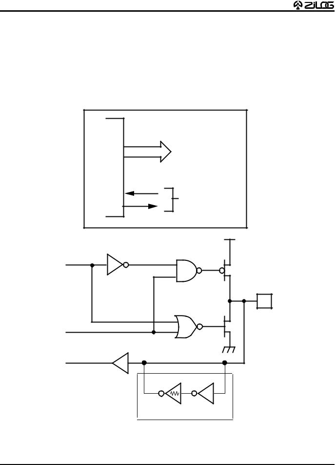
Port 1 (P17-P10). Port 1 is a multiplexed Address (A7-A0) and Data (D7-D0), CMOS compatible port. Port 1 is dedicated to the Zilog ZBus® -compatible memory interface. The operations of Port 1 are supported by the Address Strobe (/AS) and Data Strobe (/DS) lines, and by the Read/Write (R//W) and Data Memory (/DM) control lines. Data memory read/write operations are done through this
port (Figure 14). If more than 256 external locations are required, Port 0 outputs the additional lines.
Port 1 can be placed in the high-impedance state along with Port 0, /AS, /DS, and R//W, allowing the Z86LXX to share common resources in multiprocessor and DMA applications. Port1 can also be configured for standard port output mode..
8
Port 1
(I/O or AD7 - AD0)
Z86LXX
MCU
Optional
Handshake Controls
/DAV1 and RDY1
(P33 and P34)
OEN
PAD
Out
In
Auto Latch |
R ≈ 500 KΩ
Figure 14. Port 1 Configuration
20 |
P R E L I M I N A R Y |
DS96LV00800 |
 Loading...