


ZILOG Z8624312FSC, Z8624312PEC, Z8624312PSC, Z8624312VEC, Z8624312VSC Datasheet
...Z86233/243
CP96DZ81201
CUSTOMER P ROCUREMENT S PECIFICA TION
Z86233/243
CMOS Z8® 8K ROM
CONSUMER CONTROLLER PROCESSOR
FEATURES
|
ROM |
RAM |
|
Package |
Part |
Kbytes |
bytes |
I/O |
Information |
|
|
|
|
|
Z86233 |
8 |
237 |
24 |
28-pinDIP,SOIC,PLCC |
Z86243 |
8 |
236 |
32 |
40-pin DIP, |
|
|
|
|
44-pin PLCC, |
|
|
|
|
44-pin QFP |
|
|
|
|
|
■3.0-to 5.5-Volt Operating Range
■Low-Power Consumption: 40 mW (Typical @5.0V)
■0°C to +70°C Temperature Range
(–40°C to +105°C Temperature Range Available)
■Three Expanded Register File Control Registers
■Z86C33/C43 Pin and Package Compatible Version (With Addition of 4K ROM)
■32 Input/Output Lines (Three with Comparator Inputs)
(Z86243 Only)
■Vectored, Prioritized Interrupts with Programmable Polarity
■Two Comparators
■Two Programmable 8-Bit Counter/Timers, Each with a 6-Bit Programmable Prescaler
■Watch-Dog Timer (WDT)/Power-On Reset (POR)
■On-Chip Oscillator that Accepts a Crystal, Ceramic Resonator, LC, RC, or External Clock Drive
■RAM and ROM Protect
■Clock Free Watch-Dog Timer (WDT) Reset
GENERAL DESCRIPTION
The Z86233/243 Consumer Controller Processor is a member of Zilog's Z8® single-chip microcontroller family featuring enhanced wake-up circuitry, programmable Watch-Dog timers and low-EMI options. The parts provide flexible and efficient growth paths for designers currently using the 4K ROM versions of the consumer controller devices (Z86C30/C40/C33/C43).
Four address spaces, the Program Memory, Register File, Data Memory and Expanded Register File (ERF), support a wide range of memory configurations. Through the ERF, the designer has access to two additional control registers which provide extra peripheral devices, I/O ports, and register addresses.
For applications demanding powerful I/O capabilities, the Z86243 provides 32 pins dedicated to input and output. The Z86233 provides 24 pins dedicated to input and output. These lines are grouped into four ports with eight lines each, and are configurable under software control to provide timing, status signals, or parallel I/O.
With ROM/ROMless selectivity, the Z86243 provides both external memory and pre-programmed ROM, which enables this Z8 microcontroller to be used in high-volume applications, or where code flexibility is required.
Note: All Signals with a preceding front slash, "/", are active Low, e.g., B//W (WORD is active Low); /B/W (BYTE is active Low, only).
Power connections follow conventional descriptions below:
Connection |
Circuit |
Device |
|
|
|
Power |
VCC |
VDD |
Ground |
GND |
VSS |
CP96DZ81201 (8/96) |
1 |

Z86233/243
CP96DZ81201
GENERAL DESCRIPTION (Continued)
Output Input |
Vcc |
GND |
|
* |
* |
* |
* |
|
XTAL |
/AS /DS R//W /RESET |
|||||||
|
|
|
||||||
|
|
|
|
|
|
|
|
|
|
|
|
|
|
|
|
|
|
|
|
|
|
|
|
|
|
|
|
|
|
|
|
|
|
|
|
|
|
|
|
|
|
|
|
|
|
|
|
|
|
|
|
|
|
|
|
|
|
|
|
|
|
|
|
|
|
|
|
|
|
|
|
|
|
|
|
|
|
|
|
|
|
|
|
|
|
|
|
|
|
|
|
|
|
|
|
|
|
|
|
|
|
|
|
|
|
|
|
|
|
|
|
|
|
|
|
|
|
|
|
|
|
|
|
|
|
Port 3 |
|
|
|
|
|
|
|
|
|
|
|
|
|
|
|
|
|
|
Machine Timing |
|
|
R//RL† |
|||||||||||||||
|
|
|
|
|
|
|
|
|
|
|
|
|
|
|
|
|
|
|
|
|
|
|
||||||||||||||||||
|
|
|
|
|
|
|
|
|
|
|
|
|
|
|
|
|
|
|
|
|||||||||||||||||||||
|
|
|
|
|
|
|
|
|
|
|
|
|
|
|
|
|
|
|
& |
|
|
|
|
|
|
|||||||||||||||
|
|
|
|
|
|
|
|
|
|
|
|
|
|
|
|
|
|
|
|
|||||||||||||||||||||
|
|
|
|
|
|
|
|
|
|
|
|
|
|
|
|
|
|
|
|
|
|
|
|
|
|
|
|
|
|
|
|
|
|
|||||||
|
|
|
|
|
|
|
|
|
|
|
|
|
|
|
|
|
|
|
|
|
|
|
|
|
|
|
Instruction Control |
|
|
|
||||||||||
|
|
|
|
|
|
|
|
|
|
|
|
|
|
|
|
|
|
|
|
|
|
|
|
|
|
|
|
|
|
|||||||||||
|
|
|
|
|
|
|
|
|
|
|
|
|
|
|
|
|
|
|
|
|
|
|
|
|
|
|
|
|
|
|
|
|
|
|
|
|
|
|
|
|
|
|
|
|
|
|
|
|
|
|
|
|
|
|
|
|
|
|
|
|
|
|
|
|
|
|
|
|
|
|
RESET |
|
|
|
|||||||
|
|
Counter/ |
|
|
|
|
|
|
|
|
|
|
|
|
|
|
|
|
|
|
|
|
|
|
||||||||||||||||
|
|
|
|
|
|
|
|
|
|
|
|
|
|
|
|
|
|
|
|
|||||||||||||||||||||
|
|
|
|
|
|
|
|
ALU |
|
|
|
|
|
|
|
WDT, POR |
|
|
|
|||||||||||||||||||||
|
|
|
|
|
|
|
|
|
|
|
|
|
|
|
|
|||||||||||||||||||||||||
|
|
Timers (2) |
|
|
|
|
|
|
|
|
|
|
|
|
|
|
|
|
||||||||||||||||||||||
|
|
|
|
|
|
|
|
|
|
|
|
|
|
|
|
|
|
|
|
|
|
|
|
|
|
|
|
|
|
|
|
|
|
|
|
|
|
|
|
|
|
|
|
|
|
|
|
|
|
|
|
|
|
|
|
|
FLAGS |
|
|
|
|
|
|
|
|
|
|
|
|
|
|
|
|
|
|
|
|||||
|
|
Interrupt |
|
|
|
|
|
|
|
|
|
|
|
Prg. Memory |
|
|
|
|
||||||||||||||||||||||
|
|
|
|
|
|
|
|
|
|
|
|
|
|
|
|
|
|
|
|
|
|
|
|
|||||||||||||||||
|
|
|
|
|
|
|
|
|
|
|
|
|
|
|
|
|
|
|||||||||||||||||||||||
|
|
|
|
|
|
|
|
|
|
|
|
|
|
|
|
|
|
|||||||||||||||||||||||
|
|
Control |
|
|
|
|
|
|
|
|
|
|
|
|
|
|
|
|
|
|
8192 Bytes |
|
|
|
|
|||||||||||||||
|
|
|
|
|
|
|
|
|
|
|
|
|
|
|
|
|
|
|||||||||||||||||||||||
|
|
|
|
|
|
|
|
|
|
|
|
|
|
|
|
|
|
|||||||||||||||||||||||
|
|
|
|
|
|
|
|
|
|
|
|
|
|
|
|
|
|
|
|
|
|
|
|
|
|
|
|
|
|
|
|
|
|
|
|
|
||||
|
|
|
|
|
|
|
|
|
|
|
|
|
|
|
|
Register |
|
|
|
|
|
|
|
|
|
|
|
|
|
|
|
|
|
|
|
|||||
|
|
|
|
|
|
|
|
|
|
|
|
|
|
|
|
|
|
|
|
|
|
|
|
|
|
|
|
|
|
|
|
|
|
|||||||
|
|
|
|
|
|
|
|
|
|
|
|
|
|
|
|
Pointer |
|
|
|
|
|
|
|
|
|
|
|
|
|
|
|
|
|
|
|
|||||
|
Two Analog |
|
|
|
|
|
|
|
|
|
|
|
|
|
|
|
|
|
|
|
|
|
|
|
||||||||||||||||
|
Comparators |
|
|
|
|
Register File |
|
|
|
|
|
|
|
|
Program |
|
|
|
|
|||||||||||||||||||||
|
|
|
|
|
|
|
|
|
|
|
|
|
|
|
|
|
|
|
|
Counter |
|
|
|
|
||||||||||||||||
|
|
|
|
|
|
|
|
|
|
|
|
|
|
|
|
|
|
|
|
|
|
|
|
|
|
|
|
|
|
|
|
|
|
|||||||
|
|
|
|
|
|
|
|
|
|
|
|
|
|
|
|
ERF |
|
|
|
|
|
|
|
|
|
|
|
|
|
|
|
|
|
|
|
|||||
|
|
|
|
|
|
|
|
|
|
|
|
|
|
|
|
|
|
|
|
|
|
|
|
|
|
|
|
|
|
|
|
|
|
|||||||
|
|
|
|
|
|
|
|
|
|
|
|
|
|
|
|
|
|
|
|
|
|
|
|
|
|
|
|
|
|
|
|
|
|
|
|
|
|
|
|
|
|
|
|
|
|
|
|
|
|
|
|
|
|
|
|
|
|
|
|
|
|
|
|
|
|
|
|
|
|
|
|
|
|
|
|
|
|
|
|
|
|
|
|
|
|
|
|
|
|
|
|
|
|
|
|
|
|
|
|
|
|
|
|
|
|
|
|
|
|
|
|
|
|
|
|
|
|
|
|
|
|
|
|
|
|
|
|
|
|
|
|
|
|
|
|
|
|
|
|
|
|
|
|
|
|
|
|
|
|
|
|
|
|
|
|
|
|
|
|
|
|
|
|
|
|
|
|
|
|
|
|
|
|
|
|
|
|
|
|
|
|
|
|
|
|
|
|
|
|
|
|
|
|
|
|
|
|
|
|
|
|
|
|
|
|
|
|
|
|
|
|
|
|
|
|
|
|
|
|
|
|
|
|
|
|
|
|
|
|
|
|
|
|
|
|
|
|
|
|
|
|
|
|
|
|
|
|
|
|
Port 2 |
|
|
|
|
|
Port 0 |
|
|
|
|
|
Port 1 * |
|
||||||||||||||
|
|
|
|
|
|
|
|
|
|
|
|
|
|
|
|||||||||||||||||
|
|
|
|
|
|
|
|
|
|
|
|
|
|||||||||||||||||||
|
|
|
|
|
|
|
|
|
|
|
|
|
|
|
|
|
|
|
|
|
|
|
|
|
|
|
|
|
|
|
|
|
|
|
|
|
|
|
|
|
|
|
|
|
|
|
|
|
|
|
|
|
|
|
|
|
|
|
|
|
|
|
|
|
|
|
|
|
|
|
|
|
|
|
|
|
|
4 |
|
|
|
4 |
|
|
|
|
|
|
|
|
|
8 |
|
|
|
|
|
|
|
|
|
|
|
|
|
|
|
|
|
|
|
|
|
|
|
|
|
|
|||||||||
|
|
|
|
I/O |
|
|
|
|
|
|
|
|
|
|
|
|
|
|
|
|
|
|
|
||||||||
|
|
|
|
|
Address or I/O |
|
Address/Data or I/O |
||||||||||||||||||||||||
(Bit Programmable) |
(Nibble Programmable) |
|
(Byte Programmable) |
||||||||||||||||||||||||||||
* Not available on Z86233.
† Available on Z86243 44-Pin QFP and PLCC versions only.
Functional Block Diagram
2 |
CP96DZ81201 (8/96) |
Z86233/243
CP96DZ81201
PIN DESCRIPTION
P25 |
|
1 |
28 |
|
P24 |
|
28-Pin DIP/SOIC/PLCC Pin Identification |
||
|
|
|
|||||||
|
|
|
|
|
|
||||
P26 |
|
2 |
27 |
|
P23 |
Pin # |
Symbol |
Function |
Direction |
|
|
||||||||
|
|
||||||||
|
|
|
|
|
|
||||
P27 |
|
3 |
26 |
|
P22 |
1-3 |
P25-P27 |
Port 2, Pins 5,6,7 |
In/Output |
|
|
||||||||
|
|
4-7 |
P07-P04 |
Port 0, Pins 4,5,6,7 |
In/Output |
||||
P04 |
|
4 |
25 |
|
P21 |
||||
|
|
8 |
VCC |
Power Supply |
|
||||
|
|
|
|
|
|
|
|||
P05 |
|
5 |
24 |
|
P20 |
9 |
XTAL2 |
Crystal Oscillator |
Output |
|
|
||||||||
|
|
|
|
|
|
|
|
|
|
P06 |
|
6 |
23 |
|
P03 |
10 |
XTAL1 |
Crystal Oscillator |
Input |
|
|
||||||||
P07 |
|
7 |
Z86233 22 |
|
GND |
11-13 |
P33-P31 |
Port 3, Pins 1,2,3 |
Fixed Input |
|
|
||||||||
|
|
14-15 |
P35-P34 |
Port 3, Pins 4,5 |
Fixed Output |
||||
|
|
|
|
|
|
||||
VCC |
|
8 |
21 |
|
P02 |
16 |
P37 |
Port 3, Pin 7 |
Fixed Output |
|
|
||||||||
XTAL2 |
|
9 |
20 |
|
P01 |
17 |
P36 |
Port 3, Pin 6 |
Fixed Output |
|
|
||||||||
|
|
|
|
|
|
||||
XTAL1 |
|
10 |
19 |
|
P00 |
18 |
P30 |
Port 3, Pin 0 |
Fixed Input |
|
|
19-21 |
P02-P00 |
Port 0, Pins 0,1,2 |
In/Output |
||||
|
|
|
18 |
|
P30 |
||||
P31 |
|
11 |
|
22 |
GND |
Ground |
|
||
|
|
||||||||
P32 |
|
12 |
17 |
|
P36 |
23 |
P03 |
Port 0, Pins 3 |
In/Output |
|
|
24-28 |
P24-P20 |
Port 2, Pins 0,1,2,3,4 In/Output |
|||||
P33 |
|
13 |
16 |
|
P37 |
||||
|
|
|
|
|
|
||||
|
|
|
|
|
|||||
|
|
|
|
||||||
P34 |
|
14 |
15 |
|
P35 |
|
|
|
|
|
|
|
|
|
|
||||
|
|
|
|
|
|||||
|
|
|
|
|
|
|
|
|
|
28-Pin DIP Pin Configuration
P25 |
|
|
1 |
|
28 |
|
|
|
P24 |
|
|
|
|
|
|
|
|||||
P26 |
|
|
2 |
|
27 |
|
|
|
P23 |
|
|
|
|
|
|
|
|||||
P27 |
|
|
3 |
|
26 |
|
|
|
P22 |
|
|
|
|
|
|
|
|||||
P04 |
|
|
4 |
|
25 |
|
|
|
P21 |
|
|
|
|
|
|
|
|||||
P05 |
|
|
5 |
|
24 |
|
|
|
P20 |
|
|
|
|
|
|
|
|||||
P06 |
|
|
6 |
|
23 |
|
|
|
P03 |
|
|
|
|
|
|
|
|||||
P07 |
|
|
7 |
Z86233 |
22 |
|
|
|
GND |
|
|
|
|
|
|
||||||
VCC |
|
|
8 |
|
21 |
|
|
|
P02 |
|
|
|
|
|
|
|
|||||
XTAL2 |
|
|
9 |
|
20 |
|
|
|
P01 |
|
|
|
|
|
|
|
|||||
XTAL1 |
|
|
10 |
|
19 |
|
|
|
P00 |
|
|
|
|
|
|
|
|||||
P31 |
|
|
|
11 |
|
18 |
|
|
|
P30 |
|
|
|
|
|
|
|
||||
P32 |
|
|
|
12 |
|
17 |
|
|
|
P36 |
|
|
|
|
|
|
|
||||
P33 |
|
|
|
13 |
|
16 |
|
|
|
P37 |
|
|
|
|
|
|
|
||||
P34 |
|
|
|
14 |
|
15 |
|
|
|
P35 |
|
|
|
|
|
|
|
||||
|
|
|
|
|
|
|
|
|
|
|
28-Pin SOIC Pin Configuration
|
P04 |
P27 |
P26 |
P25 |
P24 |
P23 |
P22 |
|
|
4 |
|
|
1 |
|
|
26 |
|
P05XXX |
5 |
|
|
|
|
|
25 |
P21XXX |
XXXP06 |
|
|
|
|
|
|
|
XXXP20 |
XXXP07 |
|
|
Z86233 |
|
|
XXXP03 |
||
XXXVCC |
|
|
|
|
XXXGND |
|||
|
|
|
|
|
|
|
||
XT2XX |
|
|
|
|
|
|
|
P02XXX |
XT1XX |
|
|
|
|
|
|
|
P01XXX |
XXXP31 |
11 |
|
|
|
|
|
19 |
P00XXX |
|
12 |
|
|
|
|
|
18 |
|
|
P32 |
P33 |
P34 |
P35 |
P37 |
P36 |
P30 |
|
28-Pin PLCC Pin Configuration
CP96DZ81201 (8/96) |
3 |

Z86233/243
CP96DZ81201
PIN DESCRIPTION (Continued)
R//W |
|
1 |
|
||
P25 |
|
2 |
|
||
P26 |
|
3 |
|
||
P27 |
|
4 |
|
||
P04 |
|
5 |
|
||
P05 |
|
6 |
|
||
P06 |
|
7 |
|
||
P14 |
|
8 |
|
||
P15 |
|
9 |
|
||
P07 |
|
10 |
|
||
VCC |
|
11 |
|
||
P16 |
|
12 |
|
||
P17 |
|
13 |
|
||
XTAL2 |
|
14 |
|
||
XTAL1 |
|
15 |
|
||
P31 |
|
16 |
|
||
P32 |
|
17 |
|
||
P33 |
|
18 |
|
||
P34 |
|
19 |
|
||
/AS |
|
20 |
|
||
|
|
|
|
40 |
|
/DS |
|
|
||
|
39 |
|
P24 |
|
|
||
|
38 |
|
P23 |
|
|
||
|
37 |
|
P22 |
|
|
||
|
36 |
|
P21 |
|
|
||
|
35 |
|
P20 |
|
|
||
|
34 |
|
P03 |
|
|
||
|
33 |
|
P13 |
|
|
||
|
32 |
|
P12 |
|
|
||
Z86243 |
31 |
|
GND |
|
|||
DIP |
30 |
|
P02 |
|
|
||
|
29 |
|
P11 |
|
|
||
|
28 |
|
P10 |
|
|
||
|
27 |
|
P01 |
|
|
||
|
26 |
|
P00 |
|
|
||
|
25 |
|
P30 |
|
|
||
|
24 |
|
P36 |
|
|
||
|
23 |
|
P37 |
|
|
||
|
22 |
|
P35 |
|
|
||
|
21 |
|
/RESET |
|
|
||
|
|
|
|
40-Pin DIP Pin Configuration
40-Pin DIP Pin Configuaration
Pin # |
Symbol |
Function |
Direction |
|
|
|
|
1 |
R//W |
Read/Write |
Output |
2-4 |
P25-P27 |
Port 2, Pins 5, 6, 7 |
In/Output |
5-7 |
P04-P06 |
Port 0, Pins 4, 5, 6 |
In/Output |
|
|
|
|
8-9 |
P14-P15 |
Port 1, Pins 4, 5 |
In/Output |
10 |
P07 |
Port 0, Pin 7 |
In/Output |
11 |
VCC |
Power Supply |
|
12-13 |
P16-P17 |
Port 1, Pins 6, 7 |
In/Output |
14 |
XTAL2 |
Crystal Oscillator |
Output |
15 |
XTAL1 |
Crystal Oscillator |
Input |
|
|
|
|
16-18 |
P31-P33 |
Port 3, Pins 1, 2, 3 |
Input |
19 |
P34 |
Port 3, Pin 4 |
Output |
20 |
/AS |
Address Strobe |
Output |
21 |
/RESET |
Reset |
Input |
|
|
|
|
Pin # |
Symbol |
Function |
Direction |
|
|
|
|
22 |
P35 |
Port 3, Pin 5 |
Output |
23 |
P37 |
Port 3, Pin 7 |
Output |
24 |
P36 |
Port 3, Pin 6 |
Output |
|
|
|
|
25 |
P30 |
Port 3, Pin 0 |
Input |
26-27 |
P00-P01 |
Port 0, Pins 0,1 |
In/Output |
28-29 |
P10-P11 |
Port 1, Pins 0,1 |
In/Output |
|
|
|
|
30 |
P02 |
Port 0, Pin 2 |
In/Output |
31 |
GND |
Ground |
|
32-33 |
P12-P13 |
Port 1, Pins 2, 3 |
In/Output |
|
|
|
|
34 |
P03 |
Port 0, Pin 3 |
In/Output |
35-39 |
P20-P24 |
Port 2, Pins 0,1,2,3,4 |
In/Output |
40 |
/DS |
Data Strobe |
Output |
|
|
|
|
4 |
CP96DZ81201 (8/96) |
Z86233/243
CP96DZ81201
|
|
|
|
|
P20 |
|
P03 |
|
P13 |
|
P12 |
|
GND |
|
GND |
P02 |
P11 |
P10 |
P01 |
P00 |
|
|
|||||||
|
|
|
|
|
|
|
|
|
|
|
|
|
|
|
|
|
|
|
|
|
|
|
|
|
|
|
|
|
|
|
|
|
|
|
|
|
|
|
|
|
|
|
|
|
|
|
|
|
|
|
|
|
|
|
|
|
|
|
|
|
|
|
6 |
5 |
4 |
3 |
2 |
1 |
|
44 |
43 |
42 |
41 40 |
|
|
|
|
||||||||||||
|
|
|
|
|
|
|
|||||||||||||||||||||||
P21 |
|
|
7 |
|
|
|
|
|
|
|
|
|
|
|
|
|
|
|
|
|
|
|
|
39 |
|
P30 |
|||
|
|
|
|
|
|
|
|
|
|
|
|
|
|
|
|
|
|
|
|
|
|
|
|||||||
P22 |
|
|
8 |
|
|
|
|
|
|
|
|
|
|
|
|
|
|
|
|
|
|
|
|
38 |
|
P36 |
|||
|
|
|
|
|
|
|
|
|
|
|
|
|
|
|
|
|
|
|
|
|
|
|
|||||||
P23 |
|
|
9 |
|
|
|
|
|
|
|
|
|
|
|
|
|
|
|
|
|
|
|
|
37 |
|
P37 |
|||
|
|
|
|
|
|
|
|
|
|
|
|
|
|
|
|
|
|
|
|
|
|
|
|||||||
P24 |
|
|
10 |
|
|
|
|
|
|
|
|
|
|
|
|
|
|
|
|
|
|
|
|
36 |
|
P35 |
|||
|
|
|
|
|
|
|
|
|
|
|
|
|
|
|
|
|
|
|
|
|
|
|
|||||||
/DS |
|
|
11 |
|
|
|
|
|
|
|
|
Z86243 |
|
|
|
|
|
|
35 |
|
/RESET |
||||||||
|
|
|
|
|
|
|
|
|
|
|
|
|
|
|
|
|
|||||||||||||
NC |
|
|
12 |
|
|
|
|
|
|
|
|
|
|
|
|
|
|
34 |
|
R//RL |
|||||||||
|
|
|
|
|
|
|
|
|
|
PLCC |
|
|
|
|
|
|
|
||||||||||||
R//W |
|
|
13 |
|
|
|
|
|
|
|
|
|
|
|
|
|
|
33 |
|
/AS |
|||||||||
|
|
|
|
|
|
|
|
|
|
|
|
|
|
|
|
|
|
|
|
|
|
|
|||||||
P25 |
|
|
14 |
|
|
|
|
|
|
|
|
|
|
|
|
|
|
|
|
|
|
|
|
32 |
|
P34 |
|||
|
|
|
|
|
|
|
|
|
|
|
|
|
|
|
|
|
|
|
|
|
|
|
|||||||
P26 |
|
|
15 |
|
|
|
|
|
|
|
|
|
|
|
|
|
|
|
|
|
|
|
|
31 |
|
P33 |
|||
|
|
|
|
|
|
|
|
|
|
|
|
|
|
|
|
|
|
|
|
|
|
|
|||||||
P27 |
|
|
16 |
|
|
|
|
|
|
|
|
|
|
|
|
|
|
|
|
|
|
|
|
30 |
|
P32 |
|||
|
|
|
|
|
|
|
|
|
|
|
|
|
|
|
|
|
|
|
|
|
|
|
|||||||
P04 |
|
|
17 |
|
|
|
|
|
|
|
|
|
|
|
|
|
|
|
|
|
|
|
|
29 |
|
P31 |
|||
|
|
|
|
|
|
|
|
|
|
|
|
|
|
|
|
|
|
|
|
|
|
|
|||||||
|
|
|
18 |
19 |
20 |
21 |
22 |
23 |
|
24 |
25 |
26 |
27 |
28 |
|
|
|
||||||||||||
|
|
|
|
|
|
||||||||||||||||||||||||
|
|
|
|
|
|
|
|
|
|
|
|
|
|
|
|
|
|
|
|
|
|
|
|
|
|
|
|
||
|
|
|
|
|
|
|
|
|
|
|
|
|
|
|
|
|
|
|
|
|
|
|
|
|
|
|
|
|
|
|
|
|
|
|
P05 |
|
P06 |
|
P14 |
|
P15 |
|
P07 |
|
VCC |
VCC |
P16 |
P17 |
XTAL2 |
XTAL1 |
|
|
|||||||
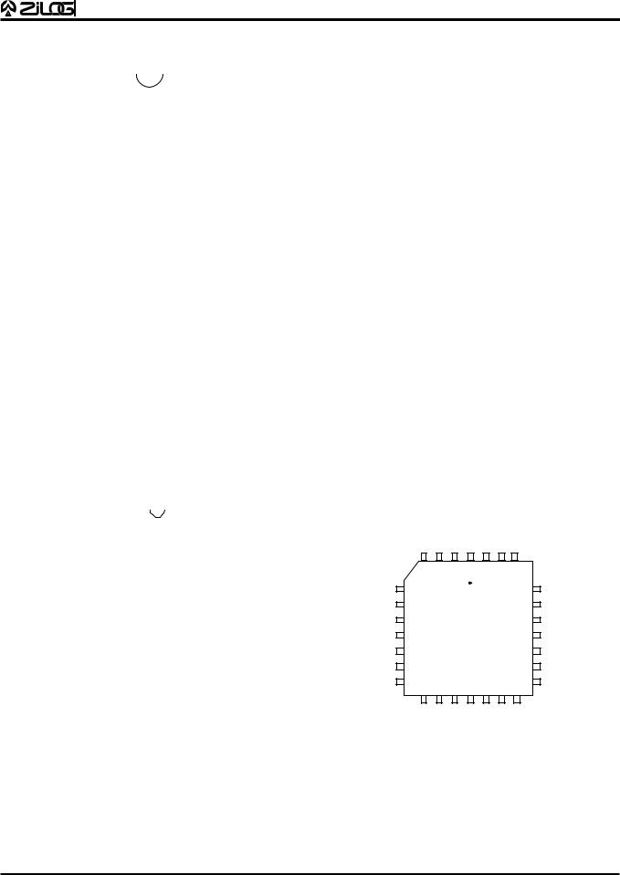
44-Pin PLCC Pin Configuration
44-Pin PLCC Pin Identification
Pin # |
Symbol |
Function |
Direction |
|
|
|
|
1 |
GND |
Ground |
|
2 |
GND |
Ground |
|
3-4 |
P12-P13 |
Port 1, Pins 2,3 |
In/Output |
5 |
P03 |
Port 0, Pin 3 |
In/Output |
6-10 |
P20-P24 |
Port 2, Pins 0,1,2,3,4 |
In/Output |
|
|
|
|
11 |
/DS |
Data Strobe |
Output |
12 |
N/C |
Not Connected |
|
13 |
R//W |
Read/Write |
Output |
14-16 |
P25-P27 |
Port 2, Pins 5,6,7 |
In/Output |
17-19 |
P04-P06 |
Port 0, Pins 4,5,6 |
In/Output |
|
|
|
|
20-21 |
P14-P15 |
Port 1, Pins 4,5 |
In/Output |
22 |
P07 |
Port 0, Pin 7 |
In/Output |
23 |
VCC |
Power Supply |
|
24 |
VCC |
Power Supply |
In/Output |
25-26 |
P16-P17 |
Port 1, Pins 6,7 |
|
|
|
|
|
Pin # |
Symbol |
Function |
Direction |
|
|
|
|
27 |
XTAL2 |
Crystal Oscillator |
Output |
28 |
XTAL1 |
Crystal Oscillator |
Input |
29-31 |
P31-P33 |
Port 3, Pins 1,2,3 |
Input |
32 |
P34 |
Port 3, Pin 4 |
Output |
33 |
/AS |
Address Strobe |
Output |
|
|
|
|
34 |
R//RL |
ROM/ROMless select |
Input |
35 |
/RESET |
Reset |
Input |
36 |
P35 |
Port 3, Pin 5 |
Output |
37 |
P37 |
Port 3, Pin 7 |
Output |
38 |
P36 |
Port 3, Pin 6 |
Output |
|
|
|
|
39 |
P30 |
Port 3, Pin 0 |
Input |
40-41 |
P00-P01 |
Port 0, Pins 0,1 |
In/Output |
42-43 |
P10-P11 |
Port 1, Pins 0,1 |
In/Output |
44 |
P02 |
Port 0, Pin 2 |
In/Output |
|
|
|
|
CP96DZ81201 (8/96) |
5 |
Z86233/243
CP96DZ81201
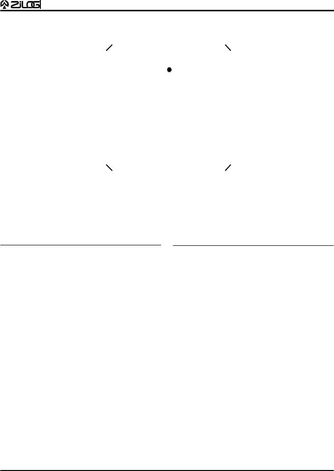
PIN DESCRIPTION (Continued)
|
|
|
|
|
|
|
|
|
|
P20 |
P03 |
P13 |
P12 |
GND |
GND |
P02 |
|
P11 |
|
P10 |
|
P01 |
|
P00 |
|
|
|
|
||||||||
|
|
|
|
|
|
|
|
|
|
|
|
|
|
|
|
|
|
|
|
|
|
|
|
|
|
|
|
|
|
|||||||
|
|
|
|
|
|
|
|
|
|
|
|
|
|
|
|
|
|
|
|
|
|
|
|
|
|
|
|
|
|
|
|
|
|
|
|
|
|
|
|
|
|
|
|
|
|
|
|
|
|
|
|
|
|
|
|
|
|
|
|
|
|
|
|
|
|
|
|
|
|
|
|
|
|
|
|
|
|
|
|
|
|
|
|
|
|
|
|
|
|
|
|
|
|
|
|
|
|
|
|
|
|
|
|
|||||||
P21 |
|
|
33 |
32 |
31 |
30 |
29 |
28 27 |
26 |
25 |
24 |
23 |
|
|
|
|
|
|
||||||||||||||||||
|
|
|
|
|
|
|
||||||||||||||||||||||||||||||
|
|
|
|
|
|
|
34 |
|
|
|
|
|
|
|
|
|
|
|
|
|
|
|
|
|
|
|
22 |
|
|
|
P30 |
|||||
P22 |
|
|
|
|
|
|
|
35 |
|
|
|
|
|
|
|
|
|
|
|
|
|
|
|
|
|
|
|
21 |
|
|
|
P36 |
||||
P23 |
|
|
|
|
|
|
|
36 |
|
|
|
|
|
|
|
|
|
|
|
|
|
|
|
|
|
|
|
20 |
|
|
|
P37 |
||||
P24 |
|
|
|
|
|
|
|
37 |
|
|
|
|
|
|
|
|
|
|
|
|
|
|
|
|
|
|
|
19 |
|
|
|
P35 |
||||
/DS |
|
|
|
|
|
|
|
38 |
|
|
|
|
|
|
|
|
Z86243 |
|
|
|
|
|
|
18 |
|
|
|
/RESET |
||||||||
NC |
|
|
|
|
|
|
|
39 |
|
|
|
|
|
|
|
|
|
|
|
|
|
|
17 |
|
|
|
R//RL |
|||||||||
R//W |
|
|
|
|
|
|
|
40 |
|
|
|
|
|
|
|
|
|
QFP |
|
|
|
|
|
|
|
|
|
|
||||||||
|
|
|
|
|
|
|
|
|
|
|
|
|
|
|
|
|
|
|
|
|
|
|
|
|
||||||||||||
P25 |
|
|
|
|
|
|
|
41 |
|
|
|
|
|
|
|
|
|
|
|
|
|
|
|
|
|
|
|
16 |
|
|
|
/AS |
||||
|
|
|
|
|
|
|
|
|
|
|
|
|
|
|
|
|
|
|
|
|
|
|
|
|
|
15 |
|
|
|
P34 |
||||||
P26 |
|
|
|
|
|
|
|
42 |
|
|
|
|
|
|
|
|
|
|
|
|
|
|
|
|
|
|
|
14 |
|
|
|
P33 |
||||
P27 |
|
|
|
|
|
|
|
43 |
|
|
|
|
|
|
|
|
|
|
|
|
|
|
|
|
|
|
|
13 |
|
|
|
P32 |
||||
P04 |
|
|
|
|
|
|
|
44 |
|
|
|
|
|
|
|
|
|
|
|
|
|
|
|
|
|
|
|
12 |
|
|
|
P31 |
||||
|
|
|
1 |
|
2 |
|
3 |
|
4 |
|
5 |
|
6 |
|
7 |
8 |
9 |
10 |
11 |
|
|
|
|
|
|
|||||||||||
|
|
|
|
|
|
|
|
|
|
|
|
|
|
|||||||||||||||||||||||
|
|
|
|
|
|
|
|
|
|
|
|
|
|
|
|
|
|
|
|
|
|
|
|
|
|
|
|
|
|
|
|
|
|
|
|
|
|
|
|
|
|
|
|
|
|
|
|
|
|
|
|
|
|
|
|
|
|
|
|
|
|
|
|
|
|
|
|
|
|
|
|
|
|
|
|
|
|
|
|
|
|
|
|
|
|
|
|
|
|
|
|
|
|
|
|
|
|
|
|
|
|
|
|
|
|
|
|
|
|
|
|
|
|
|
|
|
|
|
|
|
|
|
|
|
|
|
|
|
|
|
|
|
|
|
|
|
|
|
|
|
|
|
|
|
|
|
|
|
|
|
|
|
|
|
|
|
|
P05 |
P06 |
P14 |
P15 |
P07 |
VCC |
VCC |
|
P16 |
|
P17 |
|
XTAL2 |
|
XTAL1 |
|
|
|
|
||||||||
44-Pin QFP Pin Configuration
|
|
44-Pin QFP Pin Identification |
|
|
||
|
|
|
|
|
|
|
Pin # Symbol |
Function |
Direction |
|
Pin # Symbol |
Function |
Direction |
|
|
|
|
|
|
|
1-2 |
P05-P06 |
Port 0, Pins 5,6 |
In/Output |
3-4 |
P14-P05 |
Port 1, Pins 4,5 |
In/Output |
5 |
P07 |
Port 0, Pin 7 |
In/Output |
6-7 |
VCC |
Power Supply |
In/Output |
8-9 |
P16-P17 |
Port 1, Pins 6,7 |
|
10 |
XTAL2 |
Crystal Oscillator |
Output |
11 |
XTAL1 |
Crystal Oscillator |
Input |
|
|
|
|
12-14 P31-P33 |
Port 3, Pins 1,2,3 |
Input |
|
15 |
P34 |
Port 3, Pin 4 |
Output |
16 |
/AS |
Address Strobe |
Output |
17 |
R//RL |
ROM/ROMless select |
Input |
18 |
/RESET |
Reset |
Input |
19 |
P35 |
Port 3, Pin 5 |
Output |
20 |
P37 |
Port 3, Pin 7 |
Output |
|
|
|
|
21 |
P36 |
Port 3, Pin 6 |
Output |
22 |
P30 |
Port 3, Pin 0 |
Input |
23-24 P00-P01 |
Port 0, Pin 0,1 |
In/Output |
|
25-26 P10-P11 |
Port 1, Pins 0,1 |
In/Output |
|
27 |
P02 |
Port 0, Pin 2 |
In/Output |
28 |
GND |
Ground |
|
29 |
GND |
Ground |
|
30-31 P12-P13 |
Port 1, Pins 2,3 |
In/Output |
|
|
|
|
|
32 |
P03 |
Port 0, Pin 3 |
In/Output |
33-37 P20-24 |
Port 2, Pins 0,1,2,3,4 |
In/Output |
|
38 |
/DS |
Data Strobe |
Output |
39 |
N/C |
Not Connected |
|
40 |
R//W |
Read/Write |
Output |
41-43 P25-P27 |
Port 2, Pins 5,6,7 |
In/Output |
|
44 |
P04 |
Port 0, Pin 4 |
In/Output |
|
|
|
|
6 |
CP96DZ81201 (8/96) |
 Loading...