


ZILOG Z86E6320PSC, Z86E6320VSC, Z86E6116PSC, Z86E6116VSC, Z86E6120PSC Datasheet
...
|
P R E L I M I N A R Y |
Z86E61/E63 Z8® MCU |
|
|
WITH 16K/32K EPROM |
||
|
PRELIMINAR |
YP RODUCT S PECIFICA TION |
|
|
|
Z86E61/E63 |
|
|
CMOS Z8® 16K/32K EPROM |
|
|
MICROCONTROLLER |
FEATURES |
|
|
■ |
8-Bit CMOS Microcontroller |
■ High Voltage Protection on High Voltage Inputs |
■ 40-Pin DIP, 44-Pin PLCC Style Packages |
■ RAM and EPROM Protect |
|
■ 4.5V to 5.5V Operating Range |
■ EPROM: 16 Kbytes Z86E61 |
|
|
|
32 Kbytes Z86E63 |
■ Clock Speeds: 16 and 20 MHz |
|
|
|
|
■ 256 Bytes Register File |
■ |
Low Power Consumption: 275 mW (max) |
- 236 Bytes of General-Purpose RAM |
|
|
- 16 Bytes of Control and Status Registers |
■ |
Fast Instruction Pointer: 1.0 ms @ 12 MHz |
- 4 Bytes for Ports |
■ |
Two Standby Modes: STOP and HALT |
■ Two Programmable 8-Bit Counter/Timers Each |
|
|
with 6-Bit Programmable Prescaler |
■32 Input/Output Lines
|
|
■ |
Six Vectored, Priority Interrupts from Eight |
■ |
Full-Duplex UART |
|
Different Sources |
■ |
All Digital Inputs are TTL Levels |
■ |
On-Chip Oscillator that Accepts a Crystal, Ceramic |
|
|
|
Resonator, LC, or External Clock Drive |
■Auto Latches
GENERAL DESCRIPTION
The Z86E61/E63 microcontrollers are members of the Z8® single-chip microcontroller family with 16K/32 Kbytes of EPROM and 236 bytes of general-purpose RAM. Offered in 40-pin DIP or 44-pin PLCC package styles, these devices are pin-compatible EPROM versions of the Z86C61/ 63. The ROMless pin option is available on the 44-pin versions only.
With 4 Kbytes of ROM and 236 bytes of general-purpose RAM, the Z86E61/E63 offers fast execution, efficient use of memory, sophisticated interrupts, input/output bit manipulation capabilities, and easy hardware/software system expansion.
For applications demanding powerful I/O capabilities, the Z86E61/E63 offers 32 pins dedicated to input and output. These lines are grouped into four ports. Each port consists of eight lines, and is configurable under software control to provide timing, status signals, serial or parallel I/O with or without handshake, and an address/data bus for interfacing external memory.
The Z86E61/E63 can address both external memory and preprogrammed ROM, making it well suited for highvolume applications or where code flexibility is required.
1
P R E L I M I N A R Y |
Z86E61/E63 Z8® MCU |
WITH 16K/32K EPROM |
GENERAL DESCRIPTION (Continued)
There are three basic address spaces available to support this configuration: Program Memory, Data Memory, and 236 general-purpose registers.
To unburden the system from coping with real-time tasks such as counting/timing and serial data communication, the Z86E61/E63 offers two on-chip counter/timers with a large number of user selectable modes (Figure 1).
Notes:
All Signals with a preceding front slash, "/", are active Low, e.g., B//W (WORD is active Low); /B/W (BYTE is active Low, only).
Power connections follow conventional descriptions below:
Connection |
Circuit |
Device |
|
|
|
Power |
VCC |
VDD |
Ground |
GND |
VSS |
Output Input |
Vcc |
GND |
XTAL /AS /DS R//W /RESET |
|
|
|
|
|
|
|
|
|
|
|
|
|
|
|
|
|
|
|
|
|
|
|
|
|
|
|
|
|
|
|
|
|
|
|
|
|
|
|
|
|
|
|
|
|
|
|
|
|
|
|
|
|
|
|
|
|
|
|
|
|
|
|
|
|
|
|
|
|
|
|
|
|
|
|
|
|
|
|
|
|
|
|
|
|
|
|
|
|
|
|
|
|
|
|
|
|
|
|
|
|
|
|
|
|
|
|
|
|
|
|
|
|
|
Port 3 |
|
|
|
|
|
|
|
|
|
|
|
|
|
|
|
Machine Timing and |
|||||||||||||||||
|
|
|
|
|
|
|
|
|
|
|
|
|
|
|
|
|
|
|||||||||||||||||||
|
|
|
|
|
|
|
|
|
|
|
|
|
|
|
|
|
|
|
|
|
|
|
|
|
|
|
Instruction Control |
|||||||||
|
|
|
|
|
|
|
|
|
|
|
|
|
|
|
|
|
|
|
|
|
|
|
||||||||||||||
|
|
|
|
|
|
|
|
|
|
|
|
|
|
|
|
|
|
|
|
|
|
|
|
|
|
|
|
|
|
|
|
|
|
|
|
|
|
|
|
|
|
|
|
|
|
|
|
|
|
|
|
|
|
|
|
|
|
|
|
|
|
|
|
|
|
|
|
|
|
|
|
|
|
|
|
|
UART |
|
|
|
|
|
|
ALU |
|
|
|
|
|
|
|
|
|
|
|
|
|
|
|
|||||||||||
|
|
|
|
|
|
|
|
|
|
|
|
|
|
|
|
|
|
|
|
|
|
|
|
|||||||||||||
|
|
|
|
|
|
|
|
|
|
|
|
|
|
|
|
|
|
|
|
|
|
|
|
|
|
|
|
|
|
|
|
|
|
|
|
|
|
|
|
|
|
|
|
|
|
|
|
|
|
|
|
|
FLAGS |
|
|
|
|
|
|
|
|
|
|
|
|
|
|
|
|||||
|
|
Counter/ |
|
|
|
|
|
|
|
|
|
|
|
|
|
Prg. Memory |
|
|||||||||||||||||||
|
|
|
|
|
|
|
|
|
|
|
|
|
|
|
|
|
|
|
|
|
|
|||||||||||||||
|
|
Timers |
|
|
|
|
|
|
|
|
|
|
|
|
|
|
|
|
|
|
|
|
||||||||||||||
|
|
|
|
|
|
|
|
|
|
|
|
|
|
|
|
|
|
|
|
|
16K/32K |
|
||||||||||||||
(2) |
|
|
|
|
|
|
|
|
|
|
|
|
|
|
|
|
|
|
|
|
|
|
|
|
||||||||||||
|
|
|
|
|
|
|
|
|
|
|
|
|
|
|
|
|||||||||||||||||||||
|
|
|
|
|
|
|
|
|
|
|
|
|
|
|
|
|
|
|
|
|
|
|
|
|
|
|
|
|
|
|||||||
|
|
|
|
|
|
|
|
|
|
|
|
|
|
|
|
Register |
|
|
|
|
|
|
|
|
|
|
|
|
|
|
|
|||||
|
|
Interrupt |
|
|
|
|
|
Pointer |
|
|
|
|
|
|
|
|
|
|
|
|
|
|
|
|||||||||||||
|
|
Control |
|
|
|
|
|
|
|
|
|
|
|
|
|
|
|
|
|
|
|
Program |
|
|||||||||||||
|
|
|
|
|
|
|
Register File |
|
|
|||||||||||||||||||||||||||
|
|
|
|
|
|
|
|
|
|
|
|
|
|
|
|
256 x 8-Bit |
|
|
|
|
|
|
|
|
Counter |
|
||||||||||
|
|
|
|
|
|
|
|
|
|
|
|
|
|
|
|
|
|
|
|
|
|
|
|
|||||||||||||
|
|
|
|
|
|
|
|
|
|
|
|
|
|
|
|
|
|
|
|
|
|
|
|
|
|
|
|
|
|
|
||||||
|
|
|
|
|
|
|
|
|
|
|
|
|
|
|
|
|
|
|
|
|
|
|
|
|
|
|
|
|
|
|
|
|
|
|
|
|
|
|
|
|
|
|
|
|
|
|
|
|
|
|
|
|
|
|
|
|
|
|
|
|
|
|
|
|
|
|
|
|
|
|
|
|
|
|
|
|
|
|
|
|
|
|
|
|
|
|
|
|
|
|
|
|
|
|
|
|
|
|
|
|
|
|
|
|
|
|
|
|
|
|
|
|
|
|
|
|
|
|
|
|
|
|
|
|
|
|
|
|
|
|
|
|
|
|
|
|
|
|
|
|
|
|
|
|
|
|
|
|
|
|
|
|
|
|
|
|
|
|
|
|
|
|
|
|
|
|
|
|
|
|
|
|
|
|
|
|
|
|
|
|
|
|
|
|
|
|
|
|
Port 2 |
|
|
|
|
|
Port 0 |
|
|
|
|
|
Port 1 |
|
||||||||||||||
|
|
|
|
|
|
|
|
|
|
|
|
|
|
|
|||||||||||||||||
|
|
|
|
|
|
|
|
|
|
|
|
|
|
|
|
|
|
|
|
|
|
|
|
|
|
|
|
|
|
|
|
|
|
|
|
|
|
|
|
|
|
|
|
|
|
|
|
|
|
|
|
|
|
|
|
|
|
|
|
|
|
|
|
|
|
|
|
|
|
|
|
|
|
|
|
|
|
|
|
|
|
|
|
|
|
|
|
|
|
|
|
|
|
|
|
|
|
|
|
|
|
|
|
|
|
|
|
|
|
4 |
|
|
|
4 |
|
|
|
|
|
|
|
|
|
8 |
|
|
|
|
|
|
|
|
|
|
|
|
|
|
|
|
|
|
|
|
|
|
|
|
|
|
|||||||||
|
|
|
|
I/O |
|
|
|
|
|
|
|
|
|
|
|
|
|
|
|
|
|
|
|
||||||||
|
|
|
|
|
Address or I/O |
|
Address/Data or I/O |
||||||||||||||||||||||||
(Bit Programmable) |
(Nibble Programmable) |
|
(Byte Programmable) |
||||||||||||||||||||||||||||
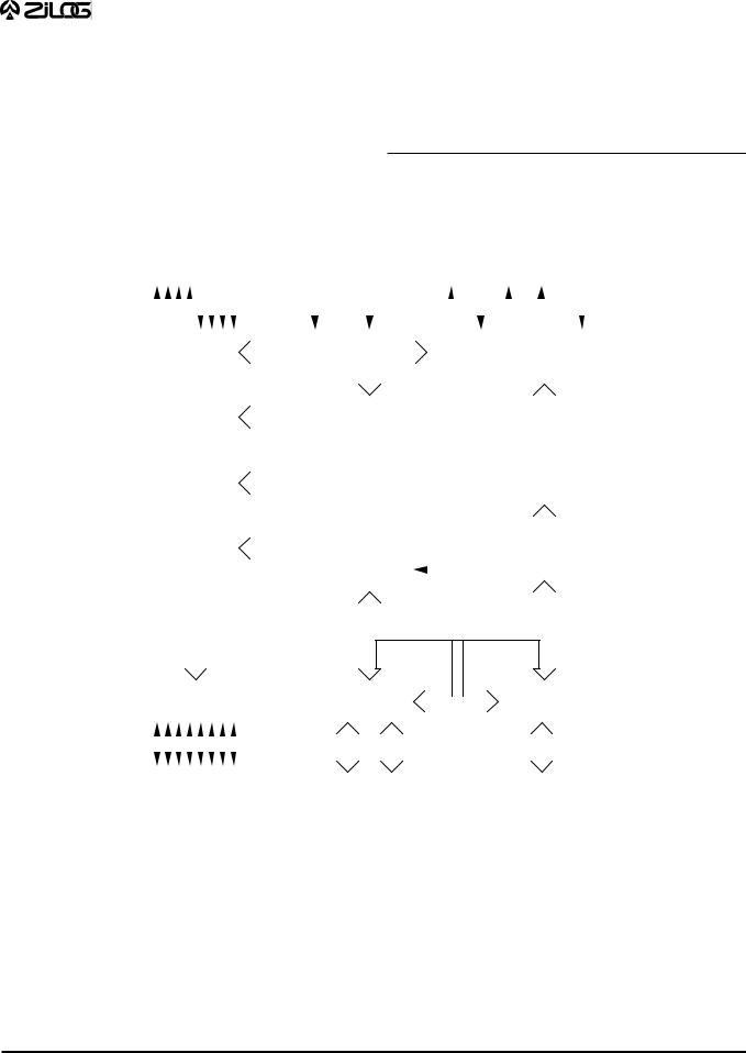
Figure 1. Z86E61/E63 Functional Block Diagram
2

P R E L I M I N A R Y |
Z86E61/E63 Z8® MCU |
WITH 16K/32K EPROM |
PIN DESCRIPTION
Standard Mode
VCC |
|
1 |
|
40 |
|
P36 |
|
|
|
||||
XTAL2 |
|
2 |
|
39 |
|
P31 |
|
|
|
||||
|
3 |
|
38 |
|
|
|
XTAL1 |
|
|
|
P27 |
||
P37 |
|
4 |
|
37 |
|
P26 |
|
|
|
||||
|
|
|
36 |
|
|
|
P30 |
|
5 |
|
|
P25 |
|
/RESET |
|
6 |
|
35 |
|
P24 |
|
|
|
||||
|
|
|
34 |
|
|
|
R//W |
|
7 |
|
|
P23 |
|
/DS |
|
8 |
|
33 |
|
P22 |
|
|
|
||||
|
|
|
32 |
|
P21 |
|
/AS |
|
9 |
Z86E61 |
|
||
P35 |
|
10 |
31 |
|
P20 |
|
|
|
|||||
GND |
|
11 |
/E63 |
30 |
|
P33 |
|
DIP |
|
||||
P32 |
|
12 |
29 |
|
P34 |
|
|
|
|
||||
|
|
|
||||
|
|
|
28 |
|
|
|
P00 |
|
13 |
|
|
P17 |
|
P01 |
|
14 |
|
27 |
|
P16 |
|
|
|
||||
|
|
|
26 |
|
|
|
P02 |
|
15 |
|
|
P15 |
|
P03 |
|
16 |
|
25 |
|
P14 |
|
|
|
||||
|
|
|
24 |
|
|
|
P04 |
|
17 |
|
|
P13 |
|
P05 |
|
18 |
|
23 |
|
P12 |
|
|
|
||||
|
|
|
22 |
|
|
|
P06 |
|
19 |
|
|
P11 |
|
P07 |
|
|
|
21 |
|
P10 |
|
20 |
|
|
|||
|
|
|
|
|
|
|
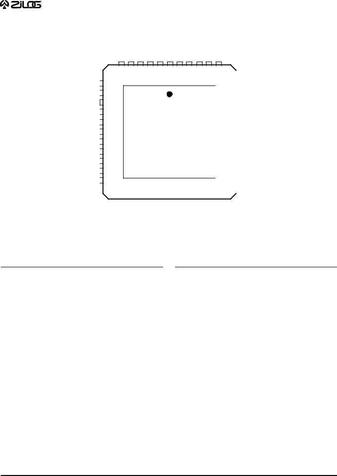
Figure 2. 40-Pin DIP Pin Configuration
Table 1. 40-Pin DIP Pin Identification
Standard Mode |
|
|
|
Pin # |
Symbol |
Function |
Direction |
|
|
|
|
1 |
VCC |
Power Supply |
Input |
2 |
XTAL2 |
Crystal, Oscillator Clock |
Output |
3 |
XTAL1 |
Crystal, Oscillator Clock |
Input |
4 |
P37 |
Port 3, Pin 7 |
Output |
5 |
P30 |
Port 3, Pin 0 |
Input |
|
|
|
|
6 |
/RESET |
Reset |
Input |
7 |
R//W |
Read/Write |
Output |
8 |
/DS |
Data Strobe |
Output |
9 |
/AS |
Address Strobe |
Output |
10 |
P35 |
Port 3, Pin 5 |
Output |
|
|
|
|
11 |
GND |
Ground |
Input |
12 |
P32 |
Port 3, Pin 2 |
Input |
13-20 |
P07-P00 |
Port 0, Pins 0,1,2,3,4,5,6,7 |
In/Output |
21-28 |
P17-P10 |
Port 1, Pins 0,1,2,3,4,5,6,7 |
In/Output |
29 |
P34 |
Port 3, Pin 4 |
Output |
|
|
|
|
30 |
P33 |
Port 3, Pin 3 |
Input |
31-38 |
P27-P20 |
Port 2, Pins 0,1,2,3,4,5,6,7 |
In/Output |
39 |
P31 |
Port 3, Pin 1 |
Input |
40 |
P36 |
Port 3, Pin 6 |
Output |
|
|
|
|
3
P R E L I M I N A R Y |
Z86E61/E63 Z8® MCU |
WITH 16K/32K EPROM |
PIN DESCRIPTION (Continued)
Standard Mode
N/C |
P30 |
6 5
/RESET 
 7 R//W
 8
8
/DS 9
/AS 
 10
10
P35 
 11
11
GND 
 12
12
P32 
 13
13
P00 
 14
14
P01 
 15
15
P02 
 16
16
R//RL 
 17
17
18 |
19 |
|
|
|
|
|
|
|
P03 |
|
P04 |
P37 |
XTAL1 |
XTAL2 |
VCC |
P36 |
P31 |
P27 |
P26 |
P25 |
|
||||||||||
4 |
|
3 |
|
2 |
|
1 |
|
44 |
43 |
42 |
41 |
40 |
|
|
|||||
|
|
|
|
|
|
||||||||||||||
|
|
|
|
|
|
|
|
|
|
|
|
|
|
|
|
39 |
|
NC |
|
|
|
|
|
|
|
|
|
|
|
|
|
|
|
|
|
|
|||
|
|
|
|
|
|
|
|
|
|
|
|
|
|
|
|
38 |
|
P24 |
|
|
|
|
|
|
|
|
|
|
|
|
|
|
|
|
|
|
|||
|
|
|
|
|
|
|
|
|
|
|
|
|
|
|
|
37 |
|
P23 |
|
|
|
|
|
|
|
|
|
|
|
|
|
|
|
|
|
|
|||
|
|
|
|
|
|
|
|
|
|
|
|
|
|
|
|
36 |
|
P22 |
|
|
|
|
|
|
|
|
|
|
|
|
|
|
|
|
|
|
|||
|
|
|
Z86E61/E63 |
|
|
|
|
35 |
|
P21 |
|||||||||
|
|
|
|
|
|
|
|
||||||||||||
|
|
|
|
|
|
|
34 |
|
P20 |
||||||||||
|
|
|
|
|
|
|
|||||||||||||
|
|
|
|
PLCC |
|
|
|
|
|
|
|
||||||||
|
|
|
|
|
|
|
|
|
|
33 |
|
P33 |
|||||||
|
|
|
|
|
|
|
|
|
|
|
|
|
|
|
|
|
|||
|
|
|
|
|
|
|
|
|
|
|
|
|
|
|
|
32 |
|
P34 |
|
|
|
|
|
|
|
|
|
|
|
|
|
|
|
|
|
|
|||
|
|
|
|
|
|
|
|
|
|
|
|
|
|
|
|
31 |
|
P17 |
|
|
|
|
|
|
|
|
|
|
|
|
|
|
|
|
|
|
|||
|
|
|
|
|
|
|
|
|
|
|
|
|
|
|
|
30 |
|
P16 |
|
|
|
|
|
|
|
|
|
|
|
|
|
|
|
|
|
|
|||
|
|
|
|
|
|
|
|
|
|
|
|
|
|
|
|
29 |
|
P15 |
|
|
|
|
|
|
|
|
|
|
|
|
|
|
|
|
|
|
|||
20 |
21 |
22 |
23 |
24 |
25 |
26 |
27 |
28 |
|
|
|||||||||
|
|
||||||||||||||||||
|
|
|
|
|
|
|
|
|
|
|
|
|
|
|
|
|
|
|
|
|
|
|
|
|
|
|
|
|
|
|
|
|
|
|
|
|
|
|
|
P05 |
P06 |
P07 |
P10 |
P11 |
P12 |
P13 |
P14 |
N/C |
|
||||||||||
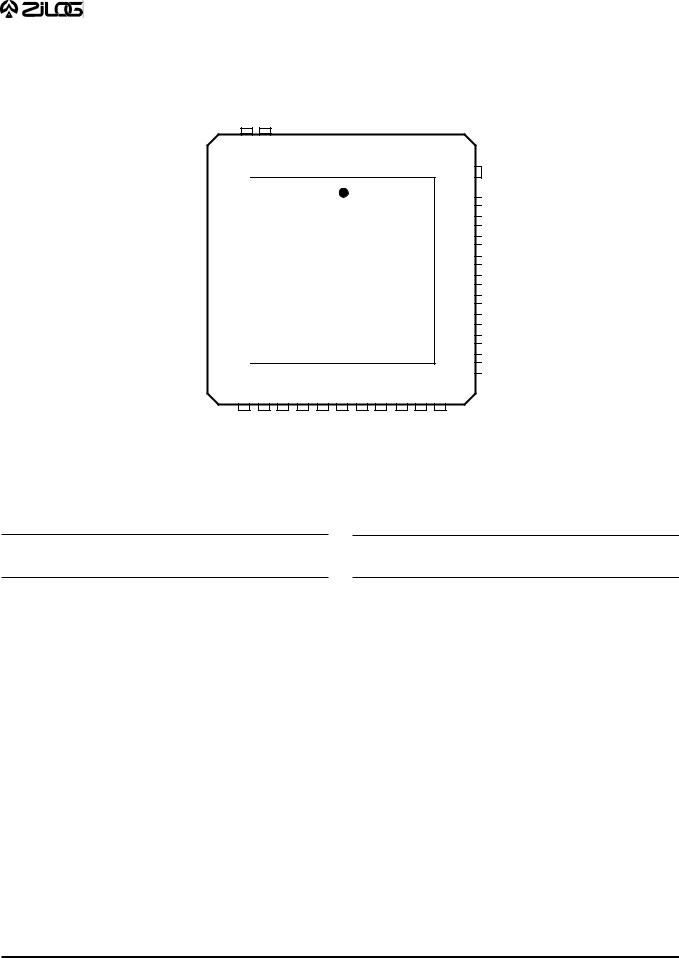
Figure 3. 44-Pin PLCC Pin Configuration
Table 2. 44-Pin PLCC Pin Identification
Standard Mode |
|
|
|
Pin # |
Symbol |
Function |
Direction |
|
|
|
|
1 |
VCC |
Power Supply |
Input |
2 |
XTAL2 |
Crystal, Osc. Clock |
Output |
3 |
XTAL1 |
Crystal, Osc. Clock |
Input |
4 |
P37 |
Port 3, Pin 7 |
Output |
|
|
|
|
5 |
P30 |
Port 3, Pin 0 |
Input |
6 |
N/C |
Not Connected |
Input |
7 |
/RESET |
Reset |
Input |
8 |
R//W |
Read/Write |
Output |
|
|
|
|
9 |
/DS |
Data Strobe |
Output |
10 |
/AS |
Address Strobe |
Output |
11 |
P35 |
Port 3, Pin 5 |
Output |
12 |
GND |
Ground |
Input |
13 |
P32 |
Port 3, Pin 2 |
Input |
|
|
|
|
Standard Mode |
|
|
|
Pin # |
Symbol |
Function |
Direction |
|
|
|
|
14-16 |
P02-P00 |
Port 0, Pins 0,1,2 |
In/Output |
17 |
R//RL |
ROM/ROMless control |
Input |
18-22 |
P07-P03 |
Port 0, Pins 3,4,5,6,7 |
In/Output |
23-27 |
P10-P14 |
Port 1, Pins 0,1,2,3,4 |
In/Output |
|
|
|
|
28 |
N/C |
Not Connected |
Input |
29-31 |
P17-P15 |
Port 1, Pins 5,6,7 |
In/Output |
32 |
P34 |
Port 3, Pin 4 |
Output |
33 |
P33 |
Port 3, Pin 3 |
Input |
|
|
|
|
34-38 |
P24-P20 |
Port 2, Pins 0,1,2,3,4 |
In/Output |
39 |
N/C |
Not Connected |
Input |
40-42 |
P27-P25 |
Port 2, Pins 5,6,7 |
In/Output |
43 |
P31 |
Port 3, Pin 1 |
Input |
44 |
P36 |
Port 3, Pin 6 |
Output |
|
|
|
|
4

P R E L I M I N A R Y |
Z86E61/E63 Z8® MCU |
WITH 16K/32K EPROM |
PIN DESCRIPTION
EPROM Mode
VCC |
|
1 |
|
40 |
|
N/C |
|
|
|
||||
XTAL2 |
|
2 |
|
39 |
|
/OE |
|
|
|
||||
XTAL1 |
|
3 |
|
38 |
|
/PGM |
|
|
|
||||
N/C |
|
4 |
|
37 |
|
A14 |
|
|
|
||||
/CE |
|
5 |
|
36 |
|
A13 |
|
|
|
||||
/RESET |
|
6 |
|
35 |
|
A12 |
|
|
|
||||
N/C |
|
7 |
|
34 |
|
A11 |
|
|
|
||||
N/C |
|
8 |
|
33 |
|
A10 |
|
|
|
||||
N/C |
|
9 |
Z86E61 |
32 |
|
A9 |
|
|
|||||
N/C |
|
10 |
31 |
|
A8 |
|
|
/E63 |
|
||||
|
|
|
|
|
|
|
GND |
|
11 |
DIP |
30 |
|
VPP |
|
|
|||||
EPM |
|
12 |
|
29 |
|
N/C |
|
|
|
||||
A0 |
|
13 |
|
28 |
|
D7 |
|
|
|
||||
A1 |
|
14 |
|
27 |
|
D6 |
|
|
|
||||
A2 |
|
15 |
|
26 |
|
D5 |
|
|
|
||||
A3 |
|
16 |
|
25 |
|
D4 |
|
|
|
||||
A4 |
|
17 |
|
24 |
|
D3 |
|
|
|
||||
A5 |
|
18 |
|
23 |
|
D2 |
|
|
|
||||
A6 |
|
19 |
|
22 |
|
D1 |
|
|
|
||||
A7 |
|
20 |
|
21 |
|
D0 |
|
|
|
||||
|
|
|
|
|
|
|
Figure 4. 40-Pin DIP Pin Configuration
Table 3. 40-Pin DIP Pin Identification
EPROM Mode |
|
|
|
Pin # |
Symbol |
Function |
Direction |
|
|
|
|
1 |
VCC |
Power Supply |
Input |
2 |
XTAL2 |
Crystal, Osc. Clock |
Output |
3 |
XTAL1 |
Crystal, Osc. Clock |
Input |
4 |
N/C |
Not Connected |
Input |
|
|
|
|
5 |
/CE |
Chip Enable |
Input |
6 |
/RESET |
Reset |
Input |
7-10 |
N/C |
Not Connected |
Input |
11 |
GND |
Ground |
Input |
|
|
|
|
12 |
EPM |
EPROM Prog Mode |
Input |
13-20 |
A7-A0 |
Address 0,1,2,3,4,5,6,7 |
Input |
21-28 |
D7-D0 |
Data 0,1,2,3,4,5,6,7 |
In/Output |
29 |
N/C |
Not Connected |
Input |
30 |
VPP |
Prog Voltage |
Input |
31-37 |
A14-A8 |
Address 8,9,10,11,12,13,14 |
Input |
38 |
/PGM |
Prog Mode |
Input |
39 |
/OE |
Output Enable |
Input |
40 |
N/C |
Not Connected |
Input |
|
|
|
|
5
P R E L I M I N A R Y |
Z86E61/E63 Z8® MCU |
WITH 16K/32K EPROM |
PIN DESCRIPTION (Continued)
EPROM Mode
N/C
6
/CE
5
N/C |
|
XTAL1 |
|
XTAL2 |
|
VCC |
|
N/C |
/OE |
/PGM |
|
A14 |
A13 |
||||
|
|
|
|
|
|
|
|
|
|
|
|
|
|
|
|
|
|
|
|
|
|
|
|
|
|
|
|
|
|
|
|
|
|
|
|
4 |
3 |
2 |
1 |
44 |
43 |
42 |
41 |
40 |
|||||||||
/RESET |
|
|
7 |
|
|
|
|
|
|
|
|
|
N/C |
|
8 |
|
|
|
|
|
|
|
|
|
|
|
|
|
|
|
|
|
|
|
|
|
||
N/C |
|
9 |
|
|
|
|
|
|
|
|
|
|
|
|
|
|
|
|
|
|
|
|
|
||
N/C |
|
10 |
|
|
|
|
|
|
|
|
|
|
|
|
|
|
|
|
|
|
|
|
|
||
N/C |
|
11 |
|
|
Z86E61/E63 |
|
|
|||||
|
|
|
|
|
|
|||||||
|
|
|
|
|
|
|
|
|||||
GND |
|
12 |
|
|
|
|
||||||
|
|
|
|
PLCC |
|
|
|
|||||
EPM |
|
|
13 |
|
|
|
|
|
|
|||
|
|
|
|
|
|
|
|
|
|
|
||
A0 |
|
14 |
|
|
|
|
|
|
|
|
|
|
|
|
|
|
|
|
|
|
|
|
|
||
A1 |
|
15 |
|
|
|
|
|
|
|
|
|
|
|
|
|
|
|
|
|
|
|
|
|
||
A2 |
|
16 |
|
|
|
|
|
|
|
|
|
|
|
|
|
|
|
|
|
|
|
|
|
||
N/C |
|
17 |
|
|
|
|
|
|
|
|
|
|
|
|
|
|
|
|
|
|
|
|
|
||
|
18 |
19 |
20 |
21 |
22 |
23 |
24 |
25 |
26 |
27 |
||
|
|
|
A3 |
A4 |
A5 |
A6 |
A7 |
D0 |
D1 |
D2 |
D3 |
D4 |
39 N/C
38  A12
A12
37 
 A11
A11
36 
 A10
A10
35 
 A9
A9
34 
 A8
A8
33 
 VPP
VPP
32 
 N/C
N/C
31 
 D7
D7
30 
 D6
D6
29 
 D5
D5
28
N/C
Figure 5. 44-Pin PLCC Pin Configuration
Table 4. 44-Pin PLCC Pin Identification
EPROM Mode |
|
Pin # Symbol Function |
Direction |
EPROM Mode |
|
Pin # Symbol Function |
Direction |
1 |
VCC |
Power Supply |
Input |
2 |
XTAL2 |
Crystal, Osc. Clock |
Input |
3 |
XTAL1 |
Crystal, Osc. Clock |
Input |
4 |
N/C |
Not Connected |
Input |
|
|
|
|
5 |
/CE |
Chip Enable |
Input |
6 |
N/C |
Not Connected |
Input |
7 |
/RESET |
Reset |
Input |
8-11 |
N/C |
Not Connected |
Input |
|
|
|
|
12 |
GND |
Ground |
Input |
13 |
EPM |
EPROM Prog Mode |
Input |
14-16 |
A0-A2 |
Address 0,1,2 |
Input |
17 |
N/C |
Not Connected |
Input |
|
|
|
|
18-22 |
A7-A3 |
Address 3,4,5,6,7 |
Input |
23-27 |
D4-D0 |
Data 0,1,2,3,4 |
In/Output |
28 |
N/C |
Not Connected |
Input |
29-31 |
D7-D5 |
Data 5,6,7 |
In/Output |
|
|
|
|
32 |
N/C |
Not Connected |
Input |
33 |
VPP |
Prog Voltage |
Input |
34-38 |
A12-A8 |
Address 8,9,10,11,12 |
Input |
39 |
N/C |
Not Connected |
Input |
|
|
|
|
40-41 |
A13-A14 |
Address 13, 14 |
Input |
42 |
/PGM |
Prog Mode |
Input |
43 |
/OE |
Output Enable |
Input |
44 |
N/C |
Not Connected |
Input |
|
|
|
|
6

P R E L I M I N A R Y |
Z86E61/E63 Z8® MCU |
WITH 16K/32K EPROM |
PIN FUNCTIONS
ROMless (input, active Low). Connecting this pin to GND disables the internal ROM and forces the device to function as a Z86C91 ROMless Z8 (see the Z86C91 product specification for more information). When left unconnected or pulled High to VCC, the device functions as a normal Z86E61/E63 EPROM version. Note: This pin is only available on the 44-pin versions of the Z86E61/E63.
/DS (output, active Low). Data Strobe is activated once for each external memory transfer. For a READ operation, data must be available prior to the trailing edge of /DS. For WRITE operations, the falling edge of /DS indicates that output data is valid.
/AS (output, active Low). Address Strobe is pulsed once at the beginning of each machine cycle. Address output is through Port 1 for all external programs. Memory address transfers are valid at the trailing edge of /AS. Under program control, /AS can be placed in the highimpedance state along with Ports 0 and 1, Data Strobe, and Read/Write.
XTAL2, XTAL1 Crystal 2, Crystal 1 (time-based input and output, respectively). These pins connect a parallelresonant crystal, ceramic resonator, LC, or any external single-phase clock to the on-chip oscillator and buffer.
R//W (output, write Low). The Read/Write signal is Low when the MCU is writing to the external program or data memory.
/RESET (input, active Low). To avoid asynchronous and noisy reset problems, the Z86E61/E63 is equipped with a reset filter of four external clocks (4TpC). If the external /RESET signal is less than 4TpC in duration, no reset occurs.
On the fifth clock after the /RESET is detected, an internal RST signal is latched and held for an internal register count of 18 external clocks, or for the duration of the external /RESET, whichever is longer. During the reset cycle, /DS is held active Low while /AS cycles at a rate of TpC/2. When /RESET is deactivated, program execution begins at location 000C (HEX). Power-up reset time must be held low for 50 ms, or until VCC is stable, whichever is longer.
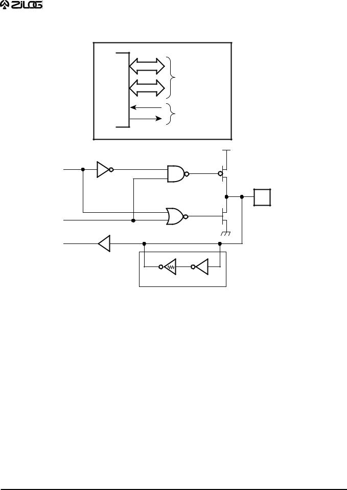
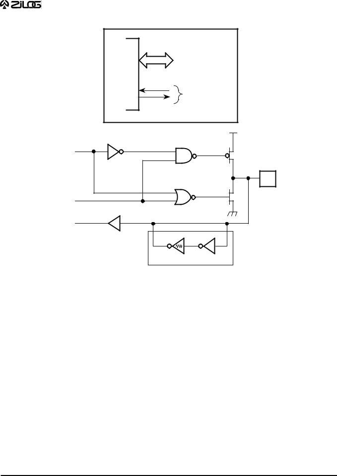
Port 0 (P07-P00). Port 0 is an 8-bit, nibble programmable, bidirectional, TTL compatible port. These eight I/O lines
can be configured under software control as a nibble I/O port, or as an address port for interfacing external memory. When used as an I/O port, Port 0 may be placed under handshake control. In this configuration, Port 3, lines P32 and P35 are used as the handshake control /DAV0 and RDY0 (Data Available and Ready). Handshake signal assignment is dictated by the I/O direction of the upper nibble P07-P04. The lower nibble must have the same direction as the upper nibble to be under handshake control.
For external memory references, Port 0 can provide address bits A11-A8 (lower nibble) or A15-A8 (lower and upper nibbles) depending on the required address space. If the address range requires 12 bits or less, the upper nibble of Port 0 can be programmed independently as I/O while the lower nibble is used for addressing. If one or both nibbles are needed for I/O operation, they must be configured by writing to the Port 0 Mode register.
In ROMless mode, after a hardware reset, Port 0 lines are defined as address lines A15-A8, and extended timing is set to accommodate slow memory access. The initialization routine can include reconfiguration to eliminate this extended timing mode (Figure 8).
Port 1 (P17-P10). Port 1 is an 8-bit, byte programmable, bidirectional, TTL compatible port. It has multiplexed Address (A7-A0) and Data (D7-D0) ports. For Z86E61/E63, these eight I/O lines can be programmed as input or output lines or are configured under software control as an address/data port for interfacing external memory. When used as an I/O port, Port 1 can be placed under handshake control. In this configuration, Port 3 lines, P33 and P34, are used as the handshake controls RDY1 and /DAV1.
Memory locations greater than 16384 (E61) or 32768 (E63) arereferencedthroughPort1.Tointerfaceexternalmemory, Port 1 must be programmed for the multiplexed Address/ Data mode. If more than 256 external locations are required, Port 0 must output the additional lines.
Port 1 can be placed in high-impedance state along with Port 0, /AS, /DS, and R//W, allowing the MCU to share common resources in multiprocessor and DMA applications. Data transfers are controlled by assigning P33 as a Bus Acknowledge input, and P34 as a Bus Request output (Figure 9).
7
P R E L I M I N A R Y |
Z86E61/E63 Z8® MCU |
WITH 16K/32K EPROM |
PIN FUNCTIONS (Continued)
4
Port 0 (I/O)
Z86E61
/E63 4
MCU
Handshake Controls
/DAV0 and RDY0
(P32 and P35)
OEN
PAD
Out
TTL Level Shifter
In
Auto Latch
R ≈ 500 kΩ
Figure 6. Port 0 Configuration
8
P R E L I M I N A R Y |
Z86E61/E63 Z8® MCU |
WITH 16K/32K EPROM |
8 |
Port 1 |
|
(AD7-AD0) |
||
Z86E61 |
||
|
||
/E63 |
|
|
MCU |
|
|
|
Handshake Controls |
|
|
/DAV1 and RDY1 |
|
|
(P33 and P34) |
OEN
PAD
Out
TTL Level Shifter
In
Auto Latch
R ≈ 500 kΩ
Figure 7. Port 1 Configuration
9

P R E L I M I N A R Y |
Z86E61/E63 Z8® MCU |
WITH 16K/32K EPROM |
PIN FUNCTIONS (Continued)
Port 2 (P27-P20). Port 2 is an 8-bit, bit programmable, bidirectional, CMOS compatible port. Each of these eight I/O lines can be independently programmed as an input or output, or globally as an open-drain output. Port 2 is always available for I/O operation. When used as an I/O port, Port 2 can be placed under handshake control. In this
configuration, Port 3 lines P31 and P36 are used as the handshake control lines /DAV2 and RDY2. The handshake signal assignment for Port 3 lines, P31 and P36, is dictated by the direction (input or output) assigned to P27 (Figure 8 and Table 5).
Z86E61 |
|
Port 2 (I/O) |
|
|
|
/E63 |
|
|
|
|
|
MCU |
|
|
|
|
|
Handshake Controls
/DAV2 and RDY2
(P31 and P36)
Open-Drain
OEN
PAD
Out
TTL Level Shifter
In
Auto Latch
R ≈ 500 kΩ
Figure 8. Port 2 Configuration
10
P R E L I M |
I N A R Y |
Z86E61/E63 Z8® MCU |
WITH 16K/32K EPROM |
||
Port 3 (P37-P30). Port 3 is an 8-bit, CMOS compatible four- |
output ports. Port 3, when used as serial I/O, is pro- |
|
fixed input and four-fixed output port. These eight I/O lines |
grammed as serial in and serial out, respectively |
|
have four-fixed (P33-P30) input and four-fixed (P37-P34) |
(Figure 9). |
|
|
|
|
|
|
|
|
Z86E61 |
|
|
|
|
Port 3 |
|
|
|
|
|
|||
|
|
|
|
|||
|
|
|
|
|||
|
|
|
|
|||
|
|
|
|
|||
/E63 |
|
|
|
|
||
MCU |
|
|
|
|
(I/O or Control) |
|
|
|
|
|
|||
|
|
|
||||
|
|
|
|
|
|
|
|
|
|
|
|
|
|
|
|
|
|
|
|
|
|
|
|
|
|
|
|
|
|
|
|
|
|
|
Figure 9. Port 3 Configuration
Port 3 is configured under software control to provide the following control functions: handshake for Ports 0 and 2 (/DAV and RDY); four external interrupt request signals
(IRQ3-IRQ0); timer input and output signals (TIN and TOUT), Data Memory Select (/DM) and EPROM control signals (P30 = /CE, P31 = /OE, P32 = EPM and P33 = VPP).
Table 5. Port 3 Pin Assignments
Pin |
I/O |
CTC1 |
Int. |
P0 HS |
P1 HS |
P2 HS |
UART |
Ext |
EPROM |
|
|
|
|
|
|
|
|
|
|
P30 |
IN |
|
IRQ3 |
|
|
|
Serial In |
|
/CE |
P31 |
IN |
TIN |
IRQ2 |
D/R |
|
D/R |
|
|
/OE |
P32 |
IN |
|
IRQ0 |
|
|
|
|
EPM |
|
P33 |
IN |
|
IRQ1 |
|
D/R |
|
|
|
VPP |
P34 |
OUT |
|
|
|
R/D |
|
|
DM |
|
P35 |
OUT |
|
|
R/D |
|
|
|
|
|
P36 |
OUT |
TOUT |
|
|
|
R/D |
Serial Out |
|
|
P37 |
OUT |
|
|
|
|
|
|
|
|
T0 |
|
|
IRQ4 |
|
|
|
|
|
|
T1 |
|
|
IRQ5 |
|
|
|
|
|
|
Notes:
HS = Handshake Signals
D = Data Available
R = Ready
11
P R E L I M I N A R Y |
Z86E61/E63 Z8® MCU |
WITH 16K/32K EPROM |
UART OPERATION
Port 3 lines, P37 and P30, are programmed as serial I/O lines for full-duplex serial asynchronous receiver/transmitter operation. The bit rate is controlled by Counter/ Timer0.
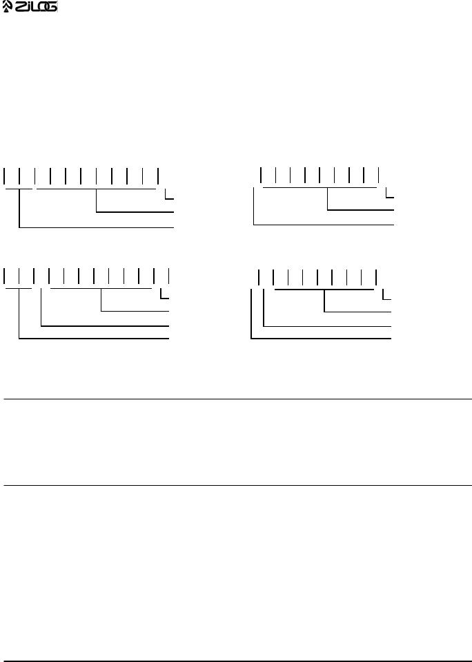
The Z86E61/E63 automatically adds a start bit and two stop bits to transmitted data (Figure 10). Odd parity is also available as an option. Eight data bits are always transmit-
ted, regardless of parity selection. If parity is enabled, the eighth bit is the odd parity bit. An interrupt request (IRQ4) is generated on all transmitted characters.
Received data must have a start bit, eight data bits, and at least one stop bit. If parity is on, bit 7 of the received data is replaced by a parity error flag. Received characters generate the IRQ3 interrupt request.
Transmitted Data (No Parity) |
|
|
|
|
|
|
|
Received Data (No Parity) |
|
|
|
|
|
|
|
||||||
SP SP |
D7 |
D6 |
D5 |
D4 |
D3 |
D2 |
D1 |
D0 |
ST |
|
SP |
D7 |
D6 D5 D4 |
D3 |
D2 |
D1 |
D0 |
ST |
|
||
|
|
|
|
|
|
|
|
|
|
|
Start Bit |
|
|
|
|
|
|
|
|
|
Start Bit |
|
|
|
|
|
|
|
|
|
|
|
|
|
|
|
|
|
|
|
|
||
|
|
|
|
|
|
|
|
|
|
|
Eight Data Bits |
|
|
|
|
|
|
|
|
|
Eight Data Bits |
|
|
|
|
|
|
|
|
|
|
|
|
|
|
|
|
|
|
|
|
|
|
|
|
|
|
|
|
|
|
|
|
|
Two Stop Bits |
|
|
|
|
|
|
|
|
|
One Stop Bit |
|
|
|
|
|
|
|
|
|
|
|
|
|
|
|
|
|
|
|
|
|
|
Transmitted Data (With Parity) |
|
|
|
|
|
|
|
Received Data (With Parity) |
|
|
|
|
|
|
|||||||
SP SP |
P |
D6 |
D5 |
D4 |
D3 |
D2 |
D1 |
D0 |
ST |
|
|
SP |
P |
D6 D5 D4 |
D3 |
D2 |
D1 |
D0 |
ST |
|
|
|
|
|
|
|
|
|
|
|
|
|
|
|
|
|
|
|
|
|
|
|
|
|
|
|
|
|
|
|
|
|
|
|
Start Bit |
|
|
|
|
|
|
|
|
|
Start Bit |
|
|
|
|
|
|
|
|
|
|
|
Seven Data Bits |
|
|
|
|
|
|
|
|
|
Seven Data Bits |
|
|
|
|
|
|
|
|
|
|
|
Odd Parity |
|
|
|
|
|
|
|
|
|
Parity Error Flag |
|
|
|
|
|
|
|
|
|
|
|
Two Stop Bits |
|
|
|
|
|
|
|
|
|
One Stop Bit |
Figure 10. Serial Data Formats
Auto Latch. The Auto Latch puts valid CMOS levels on all CMOS inputs that are not externally driven. This reduces excessive supply current flow in the input buffer when it is not driven by any source.
Note: P33-P30 inputs differ from the Z86C61/C63 in that there is no clamping diode to VCC because of the EPROM high voltage detection circuits. Exceeding the VIH maximum specification during standard operating mode may cause the device to enter EPROM mode
ADDRESS SPACE
Program Memory. The Z86E61/E63 can address 48 Kbytes (E61) or 32 Kbytes (E63) of external program memory (Figure 11). The first 12 bytes of program memory are reserved for the interrupt vectors. These locations contain six 16-bit vectors that correspond to the six available interrupts. For EPROM mode, byte 13 to byte
16383 (E61) or 32767 (E63) consists of on-chip EPROM. At addresses 16384 (E61) or 32768 (E63) and above, the Z86E61/E63 executes external program memory fetches. In ROMless mode, the Z86E61/E63 can address up to 64 Kbytes of program memory. Program execution begins at external location 000C (HEX) after a reset.
12
P R E L I M I N A R Y |
Z86E61/E63 Z8® MCU |
WITH 16K/32K EPROM |
65535 |
External |
||
|
|
||
16384 (E61) |
ROM and RAM |
||
32768 (E63) |
|
||
16383 (E61) |
|
||
32767 (E63) |
On-Chip PROM |
||
|
|
||
Location of |
12 |
|
|
First Byte of |
11 |
|
|
IRQ5 |
|||
Instruction |
|||
Executed |
10 |
|
|
IRQ5 |
|||
After RESET |
|||
|
9 |
|
|
|
IRQ4 |
||
|
8 |
|
|
|
IRQ4 |
||
|
7 |
|
|
Interrupt |
IRQ3 |
||
|
|
||
|
|
||
Vector |
6 |
IRQ3 |
|
(Lower Byte) |
|||
5 |
|
||
IRQ2 |
|||
|
|||
|
4 |
|
|
Interrupt |
IRQ2 |
||
|
|
||
|
|
||
Vector |
3 |
IRQ1 |
|
(Upper Byte) |
|||
2 |
|
||
IRQ1 |
|||
|
|||
|
1 |
|
|
|
IRQ0 |
||
|
0 |
|
|
|
IRQ0 |
||
|
|
|
|
Figure 11. Program Memory Configuration
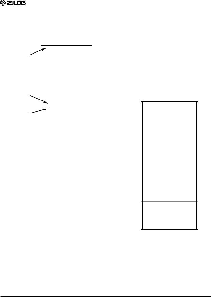
Data Memory (/DM). The EPROM version can address up to 48 Kbytes (E61) or 32 Kbytes (E63) of external data memory space beginning at location 16384 (E61) or 32768 (E63). The ROMless version can address up to 64 Kbytes of external data memory. External data memory may be included with, or separated from, the external program memory space. /DM, an optional I/O function that can be programmed to appear on pin P34, is used to distinguish between data and program memory space (Figure 12). The state of the /DM signal is controlled by the type instruction being executed. An LDC opcode references PROGRAM (/DM inactive) memory, and an LDE instruction references DATA (/DM active Low) memory.
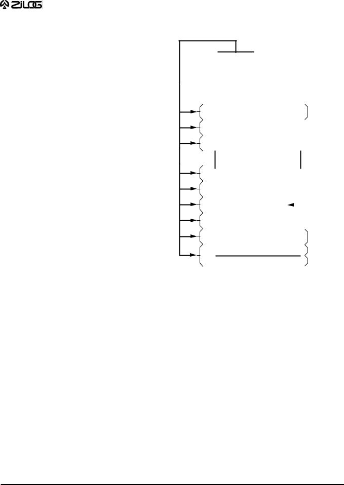
Register File. The register file consists of four I/O port registers, 236 general-purpose registers, and 16 control and status registers (Figure 13). The instructions can
access registers directly or indirectly through an 8-bit address field. The Z86E61/E63 also allows short 4-bit register addressing using the Register Pointer (Figure 14). In the 4-bit mode, the Register File is divided into 16 working register groups, each occupying 16 continuous locations. The Register Pointer addresses the starting location of the active working register group.
Stack. The Z86E61/E63 has a 16-bit Stack Pointer (R255R254) used for external stacks that reside anywhere in the data memory for the ROMless mode, but only from 16384 (E61) or 32768 (E63) to 65535 in the EPROM mode. An 8-bit Stack Pointer (R255) is used for the internal stack that resides within the 236 general-purpose registers (R239R4). The high byte of the Stack Pointer (SPH Bits 15-8) can be use as a general purpose register when using internal stack only.
65535
External
Data
Memory
32768 (E63)
16384 (E61)
16383 (E61)
32767 (E63)
Not Addressable
0
Figure 12. Data Memory Configuration
13
P R E L I M I N A R Y |
Z86E61/E63 Z8® MCU |
WITH 16K/32K EPROM |
ADDRESS SPACE (Continued)
LOCATION |
|
R255 |
|
Stack Pointer (Bits 7-0) |
|
R254 |
|
Stack Pointer (Bits 15-8) |
|
R253 |
|
Register Pointer |
|
R252 |
|
Program Control Flags |
|
R251 |
|
Interrupt Mask Register |
|
R250 |
|
Interrupt Request Register |
|
R249 |
|
Interrupt Priority Register |
|
R248 |
|
Ports 0-1 Mode |
|
|
|
R247 |
Port 3 Mode |
R246 |
|
Port 2 Mode |
|
R245 |
|
T0 Prescaler |
|
R244 |
|
Timer/Counter0 |
|
R243 |
|
T1 Prescaler |
|
|
|
R242 |
Timer/Counter1 |
R241 |
|
Timer Mode |
|
R240 |
|
Serial I/O |
|
R239 |
|
|
|
|
General-Purpose |
|
Registers |
R4 |
|
R3 |
|
Port 3 |
|
R2 |
|
Port 2 |
|
|
|
R1 |
Port 1 |
|
|
R0 |
Port 0 |
|
|
Figure 13. Register File
IDENTIFIERS SPL
SPH
RP
FLAGS
IMR
IRQ
IPR
P01M
P3M
P2M
PRE0
T0
PRE1
T1
TMR
SIO
P3
P2
P1
P0
|
r7 |
r6 |
r5 |
r4 |
r3 |
r2 |
r1 |
r0 |
|
R253 |
|||
|
|
|
|
|
|
|
|
|
|
|
(Register Pointer) |
||
|
|
|
|
|
|
|
|
|
|
||||
|
The upper nibble of the register file address |
||||||||||||
|
provided by the register pointer specifies |
|
|
|
|
||||||||
|
the active working-register group. |
|
|
|
|
|
|
||||||
FF |
|
|
|
|
|
|
|
|
|
|
|
|
|
|
|
Register Group F |
|
|
|
|
|
|
R15 to R0 |
||||
F0 |
|
|
|
|
|
|
|
|
|||||
|
|
|
|
|
|
|
|
||||||
|
|
|
|
|
|
|
|
|
|
|
|
|
|
• |
|
|
|
|
|
|
|
|
|
|
|
|
|
• |
|
|
|
|
|
|
|
|
|
|
|
|
|
• |
|
|
|
|
|
|
|
|
|
|
|
|
|
• |
|
|
|
|
|
|
|
|
|
|
|
|
|
• |
|
|
|
|
|
|
|
|
|
|
|
|
|
|
|
|
|
|
• |
|
|
|
|
|
|
|
|
|
|
|
|
|
• |
|
|
|
|
|
|
|
|
|
|
|
|
|
• |
|
|
|
|
|
|
|
|
• |
|
|
|
|
|
|
|
|
|
|
|
|
|
• |
|
|
|
|
|
|
|
|
|
|
|
The lower nibble |
|
• |
|
|
|
|
|
|
|
|
|
|
|
||
• |
|
|
|
|
|
|
|
|
|
|
|
of the register |
|
|
|
|
|
|
|
|
|
|
|
|
file address |
||
• |
|
|
Specified Working |
|
|
|
|
|
|||||
|
|
|
|
|
|
|
provided by the |
||||||
• |
|
|
Register Group |
|
|
|
|
|
|
||||
|
|
|
|
|
|
|
|
instruction points |
|||||
|
|
|
|
|
|
|
|
|
|
|
|
||
2F |
|
|
|
|
|
|
|
|
|
|
|
to the specified |
|
|
|
|
|
|
|
|
|
|
|||||
|
|
|
|
|
|
|
|
|
|
|
|
register. |
|
20 |
|
|
|
|
|
|
|
|
|
|
|
|
|
1F |
|
|
Register Group 1 |
|
|
|
|
|
|
R15 to R0 |
|||
10 |
|
|
|
|
|
|
|
|
|||||
|
|
|
|
|
|
|
|
||||||
|
|
|
|
|
|
|
|
|
|
|
|
|
|
0F |
|
|
Register Group 0 |
|
|
|
|
|
|
R15 to R4 |
|||
|
|
|
|
|
|
|
|
|
|||||
00 |
|
|
|
I/O Ports |
|
|
|
|
|
|
|
R3 to R0 |
|
|
|
|
|
|
|
|
|
|
|
||||
|
|
|
|
|
|
|
|
|
|
|
|
|
|
|
|
|
|
|
|
|
|
|
|
|
|
|
|
Figure 14. Register Pointer
14
 Loading...