


Z86319
PRELIMINARY PRODUCT SPECIFICATION
1
Z86319 |
1 |
PS/2 MOUSE CONTROLLER |
|
FEATURES
|
ROM |
RAM* |
I/O |
Voltage |
Device |
(KB) |
(Bytes) |
Lines |
Range |
|
|
|
|
|
Z86319 |
2 |
125 |
13 |
4.5V to 5.5V |
|
|
|
|
|
Note: *General-Purpose (144K Total RAM)
■0°C to + 40°C Operating Temperature Range
■Low-Power Consumption: 25 mW (Typical)
■P24-P27 Can Be Configured with a Voltage Divider During Input Mode
■On-Chip Oscillator (Tolerance = ±10%)
■Fast Instruction Pointer: 1.5 s @ 4 MHz
■ESD Protection Circuitry
■Hardwired Watch-Dog Timer (WDT)
■Excellent System Level EMI/EFT/ESD
GENERAL DESCRIPTION
The Z86319 is a member of the Z8 family of CMOS microcontrollers architecture to be used in mouse applications. These devices offer on-board pull-up and pull-down resistors, a trip-point buffer to accommodate opto-transistor outputs, and high drive ports capable of up to 10 mA current sinking per pin (3 pins maximum).
A permanently enabled Watch-Dog Timer ensures operational reliability across a broad range of mouse application environments. The precision RC oscillator filters out highfrequency noise from the oscillator input pin. When configured as inputs, P24-P27 have built in voltage dividers (25K pull-up /7.5K pull-down). The input levels are designed for connection to the emitters of the opto-transistors and switch at a voltage level of 0.4 VDD.
For applications requiring powerful I/O capabilities, the Z86319 provides dedicated input and output lines that are grouped into three ports. There are two basic address spaces available to support this configuration: Program Memory, and 125 bytes of general-purpose registers.
The Z86319 device provides two on-chip 8-bit programmable counter/timers with a large number of user-selectable modes. Each counter/timer is driven by its own 6-bit programmable prescaler. The Z86319 counter/timers off-load system real-time tasks such as counting/timing and input/output data communications for increased system efficiency.
DS97KEY1605 |
P R E L I M I N A R Y |
1 |

Z86319 |
|
PS/2 Mouse Controller |
Zilog |
GENERAL DESCRIPTION (Continued)
Input
Port 3
Counter/
Timers (2)
Interrupt
Control
Port 2
I/O
(Bit Programmable)
VDD |
|
|
GND AGND |
RCIN |
||||||||
|
|
|
|
|
||||||||
|
|
|
|
|
||||||||
|
|
|
|
|
|
|
|
|
|
|
|
|
|
|
|
|
|
|
|
|
|
|
|
|
|
|
|
|
|
|
|
|
|
|
|
|
|
|
|
|
|
|
|
|
|
|
|
|
|
|
|
|
|
|
|
|
|
|
|
|
|
Machine |
||
|
|
|
|
|
|
|
|
|
|
Timing & Inst. |
||
|
|
|
|
|
|
|
|
|
|
Control |
||
|
|
|
|
|
|
|
|
|
|
|||
|
|
|
|
|
|
|
|
|
|
|
|
|
|
|
|
|
|
|
|
|
|
|
|
|
|
|
|
ALU |
|
|
|
|
|
|
|
|||
|
|
|
|
|
|
|
|
|
||||
|
|
|
|
|
|
|
|
|
|
|
|
|
|
|
FLAG |
|
|
|
|
Prg. Memory |
|||||
|
|
|
|
|
|
2048 x 8-Bit |
||||||
|
|
|
|
|
|
|
|
|
|
|||
|
|
|
|
|
|
|
|
|
|
|
|
|
|
|
|
|
|
|
|
|
|
|
|
|
|
|
Register |
|
|
|
|
|
|
|
||||
|
|
Pointer |
|
|
|
|
|
|
|
|||
|
|
|
|
|
|
Program |
||||||
|
|
|
|
|
|
|
|
|
|
|||
Register File |
|
|
|
|
Counter |
|||||||
|
|
|
|
|||||||||
|
|
|
|
|
|
|
||||||
|
144 x 8-Bit |
|
|
|
|
|
|
|
||||
|
|
|
|
|
|
|
|
|
|
|
|
|
|
|
|
|
|
|
|
|
|
|
|
|
|
Port 0 |
WDT |
|
I/O
Figure 1. Z86319 Functional Block Diagram
2 |
P R E L I M I N A R Y |
DS97KEY1605 |

|
Z86319 |
Zilog |
PS/2 Mouse Controller |
|
|
PIN DESCRIPTIONS
P24 |
|
1 |
18 |
|
P23 |
|
|
||||||
|
||||||
P25 |
|
|
|
|
|
P22 |
|
|
|
|
|
||
|
|
|
|
|
||
P26 |
|
|
|
|
|
P21 |
|
|
|
|
|
||
|
|
|
|
|
||
P27 |
|
|
|
|
|
P20 |
|
|
18 - Pin |
|
|||
|
|
|
||||
VDD |
|
|
DIP/SOIC |
|
|
GND |
|
|
|
||||
|
|
|
||||
RCIN |
|
|
|
|
|
P02 |
|
|
|
|
|
||
AGND |
|
|
|
|
|
P01 |
|
|
|
|
|
||
|
|
|
|
|
||
P31 |
|
9 |
10 |
|
P00 |
|
|
|
|||||
|
|
|||||
GND |
|
|
P33 |
|||
|
|
|||||
|
|
|||||
|
|
|
|
|
|
|
Figure 2. 18-Pin DIP/SOIC Pin Configuration
Table 1. 18-Pin DIP/SOIC Pin Identification
Pin # |
Symbol |
Function |
Direction |
|
|
|
|
1-4 |
P24-P27 |
Port 2, Pins 4,5,6,7 |
In/Output |
|
|
|
|
5 |
VDD |
Power Supply |
Power |
6 |
RCIN |
RC Oscillator |
Input |
|
|
|
|
7 |
AGND |
Analog Ground |
Ground |
|
|
|
|
8 |
P31 |
Port 3, Pin 1 |
Input |
|
|
|
|
9 |
GND |
Ground |
Input |
|
|
|
|
10 |
P33 |
Port 3, Pin 3, |
Input |
|
|
|
|
11-13 |
P00-P02 |
Port 0, Pins 0,1,2 |
In/Output |
|
|
|
|
14 |
GND |
Ground |
Ground |
|
|
|
|
15-18 |
P20-P23 |
Port 2, Pins 0,1,2,3 |
In/Output |
|
|
|
|
DS97KEY1605 |
P R E L I M I N A R Y |
3 |
Z86319 |
|
PS/2 Mouse Controller |
Zilog |
PIN FUNCTIONS
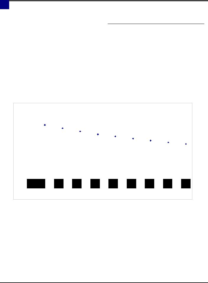
RCIN. A precision 1% resistor is connected to RCIN, generating oscillation with an internal capacitor.
Resistor values and corresponding typical frequencies are shown in Table 2 and graph chart (Figure 3).
Table 2. Resistor Values and Corresponding
Typical Frequencies
External Resistor |
Average Frequency |
|
|
14.0K |
5.01 MHz |
|
|
15.0K |
4.70 MHz |
|
|
16.0K |
4.43 MHz |
|
|
17.0K |
4.19 MHz |
|
|
18.0K |
3.97 MHz |
|
|
19.0K |
3.78 MHz |
|
|
20.0K |
3.60 MHz |
|
|
21.0K |
3.44 MHz |
|
|
22.0K |
3.30 MHz |
|
|
23.0K |
3.16 MHz |
|
|
FREQUENCY (MHz)
6
5 
4
3
2
1
0
1 4 |
1 5 |
1 6 |
1 7 |
1 8 |
1 9 |
2 0 |
2 1 |
2 2 |
2 3 |
RESISTOR VALUE (K OHMS)
Figure 3. Z86319 RC Frequency in Function of the External Resistance (typical numbers)
4 |
P R E L I M I N A R Y |
DS97KEY1605 |
|
Z86319 |
Zilog |
PS/2 Mouse Controller |
|
|
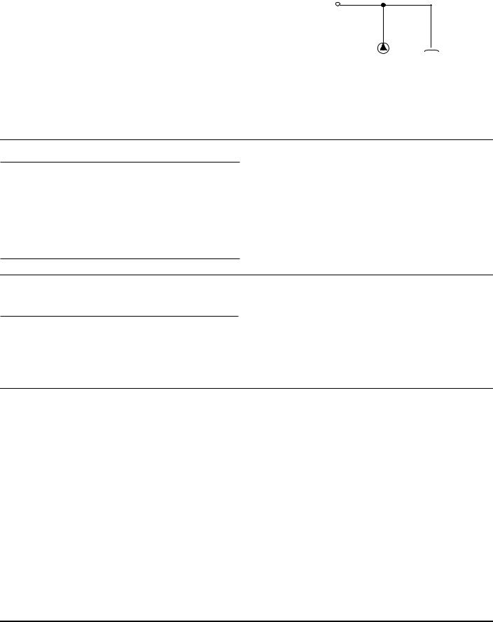
STANDARD TEST CONDITIONS
The characteristics listed below apply for standard test conditions as noted. All voltages are referenced to Ground. Positive current flows into the referenced pin (Figure 4).
From Output
Under Test
|
|
|
|
I |
|
|
|
|
|
|
|
150 pF |
|
|
|
|
|
|
|
|
|||||
|
|
|||||||||||
|
|
|
|
|
|
|
|
|
|
|
|
|
|
|
|
|
|
|
|
|
|
|
|
|
|
Figure 4. Test Load Diagram
ABSOLUTE MAXIMUM RATINGS
Sym |
Parameter |
Min |
Max |
Units |
|
|
|
|
|
VDD |
Supply Voltage* |
–0.3 |
+7 |
V |
TSTG |
Storage Temp |
–65° |
+150° |
C |
TA |
Oper Ambient |
0° |
40° |
C |
|
Temp |
|
|
|
Notes:
*Voltages on all pins with respect to Ground.
Stresses greater than those listed under Absolute Maximum Ratings may cause permanent damage to the device. This rating is a stress rating only; operation of the device at any condition above those indicated in the operational sections of these specifications is not implied. Exposure to absolute maximum rating conditions for extended periods may affect device reliability.
CAPACITANCE
TA = GND = 0V, f = 1.0 MHz, unmeasured pins returned to Ground.
Parameter |
Min |
Max |
|
|
|
Input Capacitance |
0 |
10 pF |
|
|
|
Output Capacitance |
0 |
20 pF |
|
|
|
I/O Capacitance |
0 |
25 pF |
|
|
|
VCC SPECIFICATION
VCC = 4.5V to 5.5V
Using the precision RC oscillator feature, f = 4.0 MHz ±10% under the following conditions:
■VCC = 5.0V ±10%
■Temp 0 to 40°C
■Application board capacitance:
–2.0 pF max.
–0.5 pF min.
DS97KEY1605 |
P R E L I M I N A R Y |
5 |

Z86319 |
|
PS/2 Mouse Controller |
Zilog |
DC ELECTRICAL CHARACTERISTICS
4.5V ≥ VDD ≤ 5.5V
|
|
TA = 0°C to +40°C |
|
|
|
Sym |
Parameter |
Min |
Max |
Units |
Conditions |
|
|
|
|
|
|
VIH |
Rising Input |
2.3 |
3.2 |
V |
Note 1 |
|
Schmitt-Triggered |
|
|
|
|
VIL |
Falling Input |
1.3 |
2.2 |
V |
Note 1 |
|
Schmitt-Triggered |
|
|
|
|
|
|
|
|
|
|
VIL |
Input Low Voltage CMOS Input |
|
|
V |
|
VOH |
Output High Voltage |
VDD – 0.4 |
|
V IOH = –2.0 mA; |
|
|
|
|
|
|
VDD=4.5V |
VOL1 |
Output Low Voltage |
|
0.4 |
V |
IOL = +4.0 mA; |
|
|
|
|
|
VDD=5.5V |
VOL2 |
Output Low Voltage |
|
0.8 |
V |
IOL = 10.0 mA, |
|
|
|
|
|
3 Pin Max; VDD=5.5V |
VLV |
VCC Low Voltage Protection |
2.25 |
2.95 |
V |
@ 4 MHz Max, Note 2 |
VTP |
Trip Point Voltage |
1.9 |
2.5 |
V |
P24-P27; VDD=5.5V |
|
(P24-P27) |
|
|
|
|
|
1.5 |
2.1 |
V |
VDD=4.5V |
|
|
|
||||
IIL |
Input Leakage |
–1.0 |
1.0 |
A |
VIN = 0V, or VCC |
|
|
|
|
|
Note 4 |
|
|
|
|
|
|
IOL |
Output Leakage |
–1.0 |
1.0 |
A |
VIN = 0V, or VCC |
|
|
|
|
|
Note 4 |
|
|
|
|
|
|
IDD |
Supply Current |
|
4.5 |
mA |
@ 4 MHz, Note 3; |
|
|
|
|
|
VDD=5.5V |
IDD1 |
Standby Current |
|
2.2 |
mA |
@ 4 MHz, Note 3; |
|
|
|
|
|
VDD=5.5V |
IPU |
Pull-Up Current (100K) |
–20 |
|
A |
VIH @ 1V |
|
P00-02, P31, P33 |
|
–95 |
A |
VIH @ 1V |
IPD |
Pull-Down Current (100K) |
+20 |
|
A |
VIL @ 3V |
|
P00-02, P31, P33 |
|
+85 |
A |
VIL @ 4V |
IPU |
Pull-Up Current (10K) |
–370 |
|
A |
VIL = 0V |
|
P20, P22 |
|
–670 |
A |
VIL = 0V |
Notes:
1.The min. and max. values of the Schmitt-Trigger input voltages track each other over temperature, VDD, and process variations.
2.The device is functional from VDD down to VLV voltage. The minimum operational VDD is determined by the value of the VLV voltage at ambient temperature. The VLV voltage increases as the temperature decreases.
3.All input pins are tied to GND and all output pins are floating.
6 |
P R E L I M I N A R Y |
DS97KEY1605 |
|
Z86319 |
Zilog |
PS/2 Mouse Controller |
|
|
AC ELECTRICAL CHARACTERISTICS
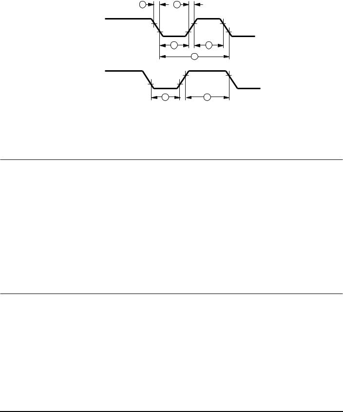
Timing Diagrams
1 |
1 |
TIN
2 |
3 |
4
IRQ N
5 |
6 |
Figure 5. Electrical Timing Diagram
|
|
|
|
TA = 0°C to +40°C |
|
|
|
No |
Symbol |
Parameter |
VDD |
Min |
Max |
Units |
Notes |
1 |
TrTin, TtTin |
Timer Input Rise and Fall Time |
5.5V |
|
100 |
ns |
1 |
|
|
|
|
|
|
|
|
2 |
TwTinL |
Timer Input Low Width |
5.5V |
70 |
|
ns |
1 |
|
|
|
|
|
|
|
|
3 |
TwTinH |
Timer Input High Width |
5.5V |
2.5TpC |
|
|
1 |
|
|
|
|
|
|
|
|
4 |
TpTin |
Timer Input Period |
5.5V |
4TpC |
|
|
1 |
|
|
|
|
|
|
|
|
5 |
TwIL |
Int. Request Input Low Time |
5.5V |
70 |
|
ns |
1,2 |
|
|
|
|
|
|
|
|
6 |
TwIH |
Int. Request Input High Time |
5.5V |
2.5TpC |
|
|
1,2 |
|
|
|
|
|
|
|
|
|
Twdt |
Watch-Dog Timer Time Out |
5.5V |
10 |
|
ms |
|
|
|
|
|
|
|
|
|
|
TPOR |
Power-On Reset Time |
5.5V |
2 |
10 |
ms |
|
|
|
|
|
|
|
|
|
|
TpC |
RC Oscillator Clock Period |
5.5V |
220 |
5000 |
ns |
|
|
|
|
|
|
|
|
|
Notes:
1.Timing Reference uses 0.9 VDD for a logic 1 and 0.1 VDD for a logic 0.
2.Interrupt request through Port 3 (P33-P31)
DS97KEY1605 |
P R E L I M I N A R Y |
7 |
 Loading...