


ZILOG Z8913820ASC, Z8913820FSC, Z8913929FSC, Z8913829ASC, Z8913829FSC Datasheet
...PRELIMINARY CUSTOMER PROCUREMENT SPECIFICATION
1
Z89138/ |
1 |
Z89139 (ROMLESS) |
|
VOICE PROCESSING CONTROLLERS
FEATURES
|
ROM |
RAM* |
I/O |
Voltage |
Device |
(KB) |
(Bytes) |
Lines |
Range |
|
|
|
|
|
Z89138 |
24 |
256 |
47 |
4.5V to 5.5V |
Z89139 |
|
256 |
47 |
4.5V to 5.5V |
|
|
|
|
|
Note: *General-Purpose
■Watch-Dog Timer and Power-On Reset
■Improved Low-Power STOP Mode
■On-Chip Oscillator that Accepts a Crystal or External Clock Drive
■Improved Global Power-Down Mode
■Low-Power Consumption - 200 mW (typical)
■Two Comparators
■RAM and ROM Protect
■On-Board Oscillator for 32.768 kHz Real-Time Clock
■Clock Speeds of 20.48 or 29.49 MHz
■16-Bit Digital Signal Processor (DSP)
■6K Word DSP Program ROM
■512 Words On-Chip DSP RAM
■8-Bit A/D Converter with up to 16 kHz Sample Rate
■10-Bit PWM D/A Converter
■Six Vectored, Prioritized Z8 Interrupts
■Three Vectored, Prioritized DSP Interrupts
■Two DSP Timers to Support Different A/D and D/A Sampling Rates
■IBM® PC-Based Development Tools
■Developer’s Toolbox for T.A.M. Applications
IBM is a registered trademark of IBM Corporation.
GENERAL DESCRIPTION
The Z89138/Z89139 is a fully integrated, dual processor controller designed for voice processing applications. The I/O control processor is a Z8® MCU with 24 KB of program memory, two 8-bit counter/timers, and up to 47 I/O pins. The DSP is a 16-bit processor with a 24-bit ALU and accumulator, 512x16 bits of RAM, single cycle instructions, and 6K words of program ROM. The chip also contains a halfflash 8-bit A/D converter with up to a 16 kHz sample rate and a 10-bit PWM D/A converter. The sampling rates for the converters are programmable. The precision of the 8- bit A/D can be extended by resampling the data at a lower rate in software. The Z8 and DSP processors are coupled by mailbox registers and an interrupt system. DSP or Z8
programs can be directed by events in each other’s domain.
The Z89139 is the ROMless version of the Z89138. However, the on-chip DSP is not ROMless.
Notes: All Signals with a preceding front slash, "/", are active Low. For example, B//W (WORD is active Low); /B/W (BYTE is active Low, only).
DS97TAD0201 |
P R E L I M I N A R Y |
1 |

Z89138/Z89139 |
|
Voice Processing Controllers |
Zilog |
GENERAL DESCRIPTION (Continued)
Power connections follow conventional descriptions below:
Connection |
Circuit |
Device |
|
|
|
Power |
VCC |
VDD |
Ground |
GND |
VSS |
Z8 Core Processor
The on-chip Z8 is Zilog’s 8-bit microcontroller core with an Expanded Register File to allow access to registermapped peripheral and I/O circuits. The Z8 offers a flexible I/O scheme, an efficient register and address space structure and a number of ancillary features, which makes it ideally suited for high-volume processing, peripheral controllers, and consumer applications.
For applications demanding powerful I/O capabilities, the Z89138 provides 47 pins dedicated to input and output. These I/O lines are grouped into six ports. Each port is configurable under software control to provide timing, status signals and parallel I/O with or without handshake.
Four basic memory resources for the Z8 are available to support a wide range of configurations: Program Memory, Register File, Data Memory, and Expanded Register File. The Z8 core processor is supported by an efficient register file that allows any of 256 on-board data and control registers to be either the source and/or the destination of almost any instruction. This unique architecture eliminates traditional microprocessor Accumulator bottlenecks and permits rapid content switching.
The Register File is composed of 236 bytes of general-pur- pose registers, four I/O port registers, and 15 control and status registers. The Expanded Register File consists of mailbox registers, WDT mode register, DSP Control register, Stop-Mode Recovery register, Port Configuration register, and the control and data registers for Port 4 and Port 5. Some of these registers are shared with the DSP.
To unburden the software from supporting real-time problems such as counting/timing and data communication, the Z8 offers two on-chip counter/timers with a large number of user-selectable modes.
Watch-Dog Timer and Stop-Mode Recovery features are software driven by setting specific bits in control registers.
STOP and HALT instructions support reduced power operation. The low-power Stop Mode allows parameter information to be stored in the register file if power fails. An external capacitor or battery will retain device memory and power the 32 kHz timer.
DSP Coprocessor
The DSP coprocessor is a second generation, 16-bit two’s- complement CMOS Digital Signal Processor (DSP). Most instructions, including multiply and accumulate, are accomplished in a single clock cycle. The processor contains two on-chip data RAM blocks of 256 words, a 6K word program ROM, 24-bit ALU, 16x16 multiplier, 24-bit Accumulator, shifter, six-level stack, three vectored interrupts and two inputs for conditional program jumps. Each RAM block contains a set of four pointers which can be incremented or decremented automatically to affect hardware looping without software overhead. The data RAMs can be simultaneously addressed and loaded to the multiplier for a true single-cycle scalar multiply.
Four external DSP registers are mapped into the expanded register file of the Z8. Communication between the Z8 and the DSP occurs through those common registers that form the mailbox registers.
The analog output is generated by a 10-bit resolution Pulse Width Modulator (PWM). The PWM output is a digital signal with CMOS output levels. The output signal has a resolution of 1 in 1024 with a sampling rate of 16 kHz (XTAL = 20.48 MHz). The sampling rate can be changed under software control and can be set at 10 and 16 kHz. The dynamic range of the PWM is from 0 to 4V.
An 8-bit resolution half-flash A/D converter is provided. The conversion is conducted with a sampling frequency of 16 kHz. (XTAL = 20.48 MHz) in order to provide oversampling. The input signal is 4V peak to peak.
Two additional timers (Timer2 and Timer3) have been added to support different sampling rates for the A/D and D/A converters. These timers are free-running counters that divide the crystal frequency to the appropriate sampling of frequency. Two DSP I/O pins: DSP0, DSP1 are provided for application.
2 |
P R E L I M I N A R Y |
DS97TAD0201 |
|
|
|
|
|
|
|
|
|
|
|
|
|
|
|
|
|
|
|
|
|
|
|
|
|
|
|
|
|
|
|
|
|
|
Z89138/Z89139 |
|
Zilog |
|
|
|
|
|
|
|
|
|
|
|
|
|
|
|
|
|
|
|
|
|
|
|
|
|
|
|
|
|
Voice Processing Controllers |
|||||
|
|
|
|
|
|
|
|
|
|
|
|
|
|
|
|
|
|
|
|
|
|
|
|
|
|
|
|
|
|
|
|
|
|
|
|
PIN DESCRIPTION |
|
|
|
|
|
|
|
|
|
|
|
|
|
|
|
|
|
|
|
|
|
|
|
|
|
|
|
|
|
|
|||||
|
P00 |
|
|
|
|
|
|
|
|
|
|
|
|
|
|
|
|
|
|
|
|
|
|
|
|
|
|
|
|
|
|
||||
|
|
|
|
|
|
Timer 0 |
|
|
|
|
|
|
|
|
|
|
|
Register File |
|
|
|
|
|
|
|
|
|||||||||
|
P01 |
|
|
|
|
|
|
|
|
|
|
|
|
|
|
Timer 1 |
|
|
|
|
|
|
|
|
|
P31 |
|
||||||||
|
P02 |
|
|
|
|
|
|
|
Capture Reg. |
|
|
|
|
|
|
|
|
|
|
|
256 x 8 Bit |
|
|
|
|
|
|
P32 |
Input |
||||||
Address |
|
|
|
|
|
|
|
|
|
|
|
|
|
|
|
|
|
|
|
|
|
|
|
|
|
|
|
|
|
|
|
||||
P03 |
|
|
|
|
|
|
|
|
|
|
|
|
|
|
|
|
|
|
|
|
|
|
|
|
|
|
|
|
|||||||
|
|
|
|
|
|
|
|
|
|
|
|
|
|
|
|
|
|
|
|
|
|
|
|
|
|
|
|
P33 |
|
||||||
or I/O |
|
|
|
|
|
Port 0 |
|
|
|
|
|
|
|
|
|
|
|
|
|
|
|
|
|
|
|
|
|
|
|
Port 3 |
|
|
|
|
|
|
|
|
|
|
|
|
|
|
|
|
|
|
|
|
|
|
|
|
|
|
|
|
|
|
|
|
|
|
|
|
|
|
|||
(Nibble |
P04 |
|
|
|
|
|
|
|
|
|
|
|
|
|
|
|
|
|
|
|
|
|
|
|
|
|
|
P34 |
|
||||||
Programmable) |
|
|
|
|
|
Register Bus |
|
|
|
|
|
|
|
|
|
|
|
|
|
|
|
|
P35 |
Output |
|||||||||||
P05 |
|
|
|
|
|
|
|
|
|
Internal Address Bus |
|
|
|
|
|
|
|
|
|
||||||||||||||||
|
|
|
|
|
|
|
|
|
24 Kbytes |
|
|
|
|
|
|
|
|
|
|
|
P36 |
|
|||||||||||||
|
P06 |
|
|
|
|
|
|
Program |
|
|
|
|
|
|
|
|
|
Z8 Core |
|
|
|
|
|
|
P37 |
|
|||||||||
|
P07 |
|
|
|
|
|
|
|
|
|
|
|
|
|
|
|
|
|
|
|
|
|
|||||||||||||
|
|
|
|
|
|
|
|
ROM |
|
|
|
|
|
|
|
|
|
|
|
|
|
|
|
|
|
|
|||||||||
|
|
|
|
|
|
|
|
|
|
|
|
|
|
|
|
|
|
|
|
|
|
|
|
|
|
|
|
|
|
||||||
|
|
|
|
|
|
|
|
|
|
|
|
(Z89138) |
Internal Data Bus |
|
|
|
|
|
|
|
|
|
|
|
|||||||||||
|
|
|
|
|
|
|
|
|
|
|
|
|
|
|
|
|
|
|
|
|
|
|
|||||||||||||
|
P10 |
|
|
|
|
P40 |
|
|
P11 |
|
|
|
Expanded |
P41 |
|
|
P12 |
|
|
|
P42 |
I/O |
|
Address/Data |
|
Expanded Register |
|
Register Bus |
|||
P13 |
|
|
P43 |
||||
|
|
|
(Bit |
||||
or I/O |
Port 1 |
File |
|
Port 4 |
|||
P14 |
|
P44 |
Programmable) |
||||
(Byte |
|
(Z8) |
|
|
|||
P15 |
|
|
|
P45 |
|
||
Programmable) |
|
|
|
|
|
||
|
P16 |
|
|
|
|
P46 |
|
|
P17 |
|
Peripheral |
Extended Bus of the DSP |
P47 |
|
|
|
|
|
Register |
|
|
|
|
|
|
|
(DSP) |
|
|
|
|
|
P20 |
|
|
256 Word |
256 Word |
P50 |
|
|
P21 |
|
mailbox |
P51 |
|
||
|
|
RAM 0 |
RAM 1 |
|
|||
|
P22 |
|
P52 |
|
|||
I/O |
|
|
|
|
I/O |
||
P23 |
|
|
|
|
P53 |
||
(Bit |
Port 2 |
|
|
Port 5 |
(Bit |
||
P24 |
|
|
P54 |
||||
Programmable) |
|
Internal Address Bus |
|
Programmable) |
|||
|
P25 |
|
6K Words |
|
|
P55 |
|
|
P26 |
|
Program |
DSP Core |
P56 |
|
|
|
P27 |
|
ROM |
|
|
P57 |
|
|
|
|
Internal Data Bus |
|
|
|
|
|
|
|
INT 1 |
|
|
|
|
RMLS |
|
|
|
|
|
|
|
|
|
|
|
|
|
|
|
INT 2 |
|
|
|
|
|
|
|
|
|
|
|
|
|
|
DSP0 |
/AS |
|
|
|
|
|
Ext. |
|
|
|
|
|
|
|
|
|
|
|
|
|
|
|
|
DSP Port |
|
|
|
DSP1 |
||||
|
|
|
|
|
|
|
|
|
|
|
|
|
|
|
|
|
|
|
|
|
|
|
|
|
|||||||
/DS |
|
|
|
|
|
Memory |
|
|
|
|
|
|
|
|
Extended Bus of the DSP |
|
|
|
|
|
|||||||||||
R/W |
|
|
|
|
|
Control |
|
Timer 2 |
|
Timer 3 |
|
|
|
|
|
|
|
|
|
|
PWM |
|
|
|
|
||||||
|
|
|
|
|
|
|
|
|
|
|
|
|
|
|
|
|
|
|
|
|
|
|
|||||||||
XTAL1 |
|
|
|
|
|
|
|
|
OSC |
|
|
|
|
|
|
|
|
|
|
|
|
|
|
|
|
(10-Bit) |
|
|
|
PWM |
|
|
|
|
|
|
|
|
|
|
|
|
|
|
|
|
|
|
|
|
|
|
|
|
|
|
|
|
|
||||
|
|
|
|
|
|
|
|
|
|
|
|
|
|
|
|
|
|
|
|
|
|
|
|
|
|
|
|
||||
XTAL2 |
|
|
|
|
|
|
|
|
|
|
|
|
|
|
|
|
|
|
|
|
|
|
|
|
|
AN IN |
|||||
|
|
|
|
|
|
|
|
|
|
|
|
|
|
|
|
|
|
|
|
|
|
|
|
|
|
||||||
VDD |
|
|
|
|
|
|
|
|
|
|
|
|
|
|
|
|
|
|
|
|
|
|
|
|
ADC |
|
|
|
AN VDD |
||
|
|
|
|
|
|
|
|
|
|
|
|
|
|
|
|
|
|
|
|
|
|
|
|
||||||||
GND |
|
|
|
|
|
|
|
|
Power |
|
|
|
|
|
|
|
|
|
|
|
|
|
|
|
|
|
|
|
AN GND |
||
|
|
|
|
|
|
|
|
|
|
|
|
|
|
|
|
|
|
|
|
|
|
|
|
(8-Bit) |
|
|
|
||||
|
|
|
|
|
|
|
|
|
|
|
|
|
|
|
|
|
|
|
|
|
|
||||||||||
/RESET |
|
|
|
|
|
|
|
|
|
|
|
|
|
|
|
|
|
|
|
|
|
|
|
|
|
|
|
VREF+ |
|||
|
|
|
|
|
|
|
|
|
|
|
|
|
|
|
|
|
|
|
|
|
|
|
|
|
|
||||||
|
|
|
|
|
|
|
|
|
|
|
|
|
|
|
|
|
|
|
|
|
|
|
|
|
|
|
|
|
|
|
VREF- |
|
|
|
|
|
|
|
|
|
|
|
|
|
|
|
|
|
|
|
|
|
|
|
|
|
|
|
|
|
|
|
|
OSC1 |
|
|
|
|
|
|
|
|
32 kHz |
|
|
|
|
|
|
|
|
|
|
|
|
|
|
|
|
|
|
|
|
|
|
|
|
|
|
OSC |
|
|
|
|
|
|
|
|
|
|
|
|
|
|
|
|
|
|
|
|
|
|
|||||
OSC2 |
|
|
|
|
|
|
|
|
|
|
|
|
|
|
|
|
|
|
|
|
|
|
|
|
|
|
|||||
|
|
|
|
|
|
|
|
|
|
|
|
|
|
|
|
|
|
|
|
|
|
|
|
|
|||||||
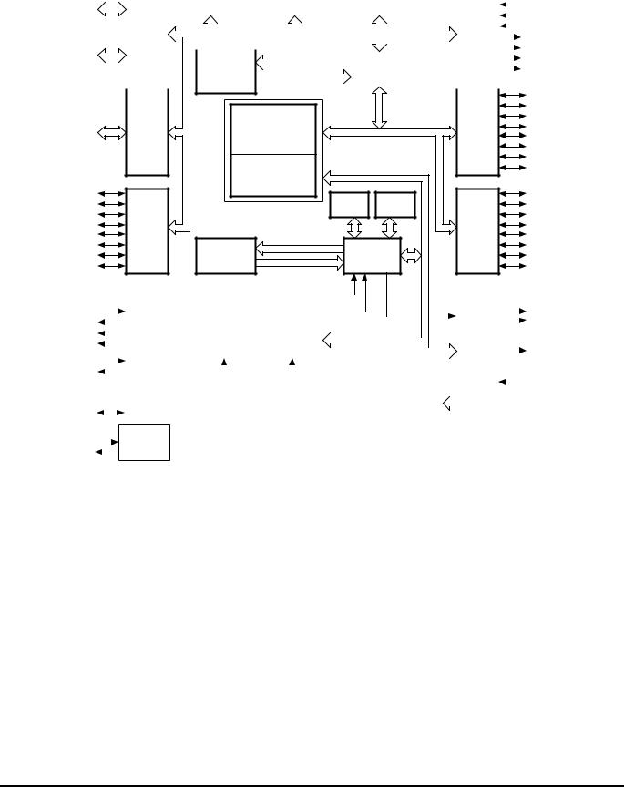
Figure 1. Z89138/139 Functional Block Diagram
DS97TAD0201 |
P R E L I M I N A R Y |
3 |
Z89138/Z89139 |
|
Voice Processing Controllers |
Zilog |
PIN DESCRIPTION (Continued)
P06
P05
P04
P03
P02
P01
P00
GND
P17
P16
P15
P14
P13
P12
P11
P10
GND
AGND VREFANIN
P07 NC NC VCC NC NC NC NC NC NC NC NC NC NC NC NC NC NC NC NC NC NC NC NC |
NC OSC02 OSC01 GND NC NC |
|
||||||
80 |
75 |
70 |
65 |
60 |
55 |
51 |
|
|
81 |
|
|
|
|
|
|
50 |
NC |
|
|
|
|
|
|
|
|
NC |
|
|
|
|
|
|
|
|
NC |
85 |
|
|
|
|
|
|
|
VCC |
|
|
|
|
|
|
|
P51 |
|
|
|
|
|
|
|
|
45 |
P50 |
|
|
|
|
|
|
|
|
P47 |
|
|
|
|
|
|
|
|
P46 |
90 |
|
|
|
100-Pin QFP |
|
|
|
P45 |
|
|
|
|
|
|
P44 |
||
|
|
|
|
|
|
|
40 |
P43 |
|
|
|
|
|
|
|
|
P42 |
|
|
|
|
|
|
|
|
P41 |
95 |
|
|
|
|
|
|
|
P40 |
|
|
|
|
|
|
|
P27 |
|
|
|
|
|
|
|
|
35 |
P26 |
|
|
|
|
|
|
|
|
P25 |
|
|
|
|
|
|
|
|
P24 |
100 |
|
|
|
|
|
|
P23 |
|
|
|
|
|
|
31 |
P22 |
||
1 |
5 |
|
10 |
15 |
20 |
25 |
30 |
|
VREF+ |
ANVDD GND PWM RMLS |
DSP1 DSP0 |
/AS /DS R//W NC P57 |
P56 P55 P54 VCC XTAL2 XTAL1 P53 |
P52 P37 P36 P35 P34 |
P33 P32 P31 /RESET P20 |
P21 |
|
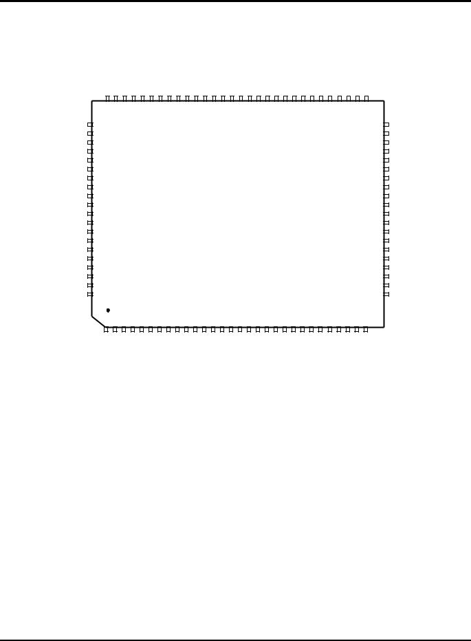
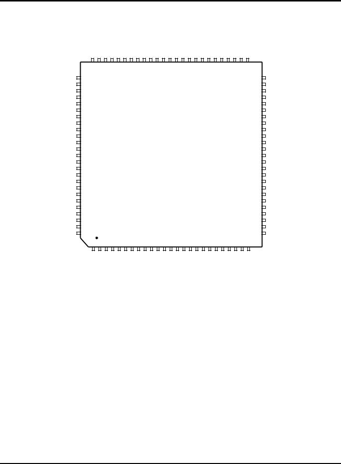
Figure 2. Z89138 100-Pin QFP Pin Configuration
4 |
P R E L I M I N A R Y |
DS97TAD0201 |

|
|
|
Z89138/Z89139 |
|
Zilog |
|
|
Voice Processing Controllers |
|
|
|
|
||
|
Table 1. Z89138 100-Pin QFP Pin Identification |
|||
|
|
|
|
|
I/O Port |
Pin |
|
|
|
Symbol |
Number |
Direction |
Function |
|
|
|
|
|
|
GND |
3, 53, 88, 97 |
|
Digital Ground |
|
|
|
|
|
|
VCC |
16, 47, 77 |
|
Digital VCC = +5V |
|
VREF+ |
1 |
Input/Output |
Analog Voltage Ref+ |
|
|
|
|
|
|
ANVDD |
2 |
|
Analog VDD |
|
PWM |
4 |
Output |
PWM Output |
|
|
|
|
|
|
RMLS |
5 |
Input |
Control Input |
|
|
|
|
|
|
DSP1-0 |
6, 7 |
Output |
DSP User Output 1, 0 |
|
|
|
|
|
|
/AS |
8 |
Output |
Address Strobe |
|
|
|
|
|
|
/DS |
9 |
Output |
Data Strobe |
|
|
|
|
|
|
R//W |
10 |
Output |
Read/Write |
|
|
|
|
|
|
NC |
11 |
|
No Connection |
|
|
|
|
|
|
P57-P54 |
12-15 |
Input/Output |
Port 5 Bit 7-4 |
|
|
|
|
|
|
XTAL2 |
17 |
Output |
Crystal Output (20.48 or 29.49 MHz) |
|
|
|
|
|
|
XTAL1 |
18 |
Input |
Crystal Input (20.48 or 29.49 MHz) |
|
|
|
|
|
|
P53-P52 |
19, 20 |
Input/Output |
Port 5 Bit 3-2 |
|
|
|
|
|
|
P37-P34 |
21-24 |
Output |
Port 3 Bit 7-4 |
|
|
|
|
|
|
P33-P31 |
25-27 |
Input |
Port 3 Bit 3-1 |
|
|
|
|
|
|
/RESET |
28 |
Input/Output |
Reset |
|
|
|
|
|
|
P20-P27 |
29-36 |
Input/Output |
Port 2, Bit 0-7 |
|
|
|
|
|
|
P40-P47 |
37-44 |
Input/Output |
Port 4, Bit 0-7 |
|
|
|
|
|
|
P50-P51 |
45, 46 |
Input/Output |
Port 5, Bit 0-1 |
|
|
|
|
|
|
NC |
48-52 |
|
No Connection |
|
|
|
|
|
|
OSC1 |
54 |
Input |
Crystal Input (32.768 kHz) |
|
|
|
|
|
|
OSC2 |
55 |
Output |
Crystal Output (32.768 kHz) |
|
|
|
|
|
|
NC |
56-76 |
|
No Connection |
|
|
|
|
|
|
NC |
78, 79 |
|
No Connection |
|
|
|
|
|
|
P07-P00 |
80-87 |
Input/Output |
Port 0, Bit 7-0 |
|
|
|
|
|
|
P17-P10 |
89-96 |
Input/Output |
Port 1, Bit 7-0 |
|
|
|
|
|
|
ANGND |
98 |
|
Analog GND |
|
|
|
|
|
|
VREF- |
99 |
Input |
Analog Voltage Ref- |
|
|
|
|
|
|
ANIN |
100 |
Input |
Analog Input |
|
|
|
|
|
|
DS97TAD0201 |
P R E L I M I N A R Y |
5 |
Z89138/Z89139 |
|
Voice Processing Controllers |
Zilog |
PIN DESCRIPTION (Continued)
|
VCC NC NC NC NC NC NC NC NC NC NC NC NC NC NC NC NC |
NC NC NC NC NC OSC2 OSC1 GND |
||||
|
75 |
70 |
65 |
60 |
55 |
51 |
NC |
76 |
|
|
|
|
50 |
NC |
|
|
|
|
|
|
P07 |
|
|
|
|
|
|
P06 |
|
|
|
|
|
|
P05 |
80 |
|
|
|
|
|
P04 |
|
|
|
|
|
45 |
P03 |
|
|
|
|
|
|
P02 |
|
|
|
|
|
|
P01 |
|
|
|
|
|
|
P00 |
85 |
|
|
|
|
|
GND |
|
|
|
|
40 |
|
|
|
|
|
|
||
P17 |
|
|
100-Pin VQFP |
|
|
|
P16 |
|
|
|
|
||
|
|
|
|
|
|
|
P15 |
|
|
|
|
|
|
P14 |
|
|
|
|
|
|
P13 |
90 |
|
|
|
|
35 |
P12 |
|
|
|
|
|
|
P11 |
|
|
|
|
|
|
P10 |
|
|
|
|
|
|
GND |
|
|
|
|
|
|
AGND |
95 |
|
|
|
|
30 |
VREF- |
|
|
|
|
|
|
|
|
|
|
|
|
|
ANIN |
|
|
|
|
|
|
VREF+ |
100 |
|
|
|
|
|
ANVDD |
|
|
|
|
26 |
|
|
1 |
5 |
10 |
15 |
20 |
25 |
|
GND PWM RMLS DSP1 |
DSP0 /AS |
/DS R//W NC P57 P56 |
P55 P54 VCC XTAL2 XTAL1 P53 |
P52 P37 P36 P35 P34 |
P33 P32 P31 |
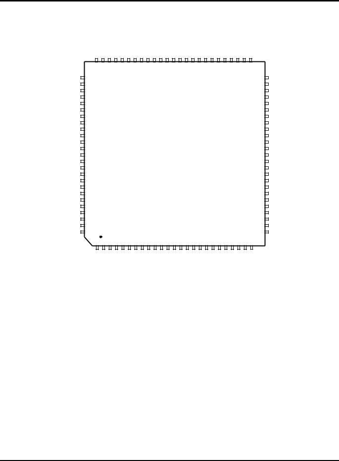
Figure 3. Z89138 100-Pin VQFP Pin Configuration
NC
NC
NC
NC
NC
VCC P51 P50 P47 P46 P45 P44 P43 P44 P45 P46 P47 P50 P51 VCC NC NC NC NC NC
6 |
P R E L I M I N A R Y |
DS97TAD0201 |

|
|
|
Z89138/Z89139 |
|
Zilog |
|
|
Voice Processing Controllers |
|
|
|
|
|
|
|
Table 2. Z89138 100-Pin VQFP Pin Identification |
|
|
|
|
|
|
|
|
I/O Port |
Pin |
|
|
|
Symbol |
Number |
Direction |
Symbol |
|
|
|
|
|
|
GND |
1, 51, 86, 95 |
|
Digital Ground |
|
|
|
|
|
|
VCC |
14, 45, 75 |
|
Digital VCC = +5V |
|
VREF+ |
99 |
Input/Output |
Analog Voltage Ref+ |
|
|
|
|
|
|
ANVDD |
100 |
|
Analog VDD |
|
PWM |
2 |
Output |
PWM Output |
|
|
|
|
|
|
RMLS |
3 |
Input |
Control Input |
|
|
|
|
|
|
DSP1-0 |
4, 5 |
Output |
DSP User Output 1, 0 |
|
|
|
|
|
|
/AS |
6 |
Output |
Address Strobe |
|
|
|
|
|
|
/DS |
7 |
Output |
Data Strobe |
|
|
|
|
|
|
R//W |
8 |
Output |
Read/Write |
|
|
|
|
|
|
NC |
9 |
|
No Connection |
|
|
|
|
|
|
P57-P54 |
10-13 |
Input/Output |
Port 5 Bit 7-4 |
|
|
|
|
|
|
XTAL2 |
15 |
Output |
Crystal Output (20.48 or |
|
|
|
|
29.49 MHz) |
|
|
|
|
|
|
XTAL1 |
16 |
Input |
Crystal Input (20.48 or 29.49 |
|
|
|
|
MHz) |
|
|
|
|
|
|
P53-P52 |
17, 18 |
Input/Output |
Port 5 Bit 3-2 |
|
|
|
|
|
|
P37-P34 |
19-22 |
Output |
Port 3 Bit 7-4 |
|
|
|
|
|
|
P33-P31 |
23-25 |
Input |
Port 3 Bit 3-1 |
|
|
|
|
|
|
/RESET |
26 |
Input/Output |
Reset |
|
|
|
|
|
|
P20-P27 |
27-34 |
Input/Output |
Port 2, Bit 0-7 |
|
|
|
|
|
|
P40-P47 |
35-42 |
Input/Output |
Port 4, Bit 0-7 |
|
|
|
|
|
|
P50-P51 |
43, 44 |
Input/Output |
Port 5, Bit 0-1 |
|
|
|
|
|
|
NC |
46-50 |
|
No Connection |
|
|
|
|
|
|
OSC1 |
52 |
Input |
Crystal Input (32.768 kHz) |
|
|
|
|
|
|
OSC2 |
53 |
Output |
Crystal Output (32.768 kHz) |
|
|
|
|
|
|
NC |
54-74 |
|
No Connection |
|
|
|
|
|
|
NC |
76, 77 |
|
No Connection |
|
|
|
|
|
|
P07-P00 |
78-85 |
Input/Output |
Port 0, Bit 7-0 |
|
|
|
|
|
|
P17-P10 |
87-94 |
Input/Output |
Port 1, Bit 7-0 |
|
|
|
|
|
|
ANGND |
96 |
|
Analog GND |
|
|
|
|
|
|
VREF- |
97 |
Input |
Analog Voltage Ref- |
|
|
|
|
|
|
ANIN |
98 |
Input |
Analog Input |
|
|
|
|
|
|
DS97TAD0201 |
P R E L I M I N A R Y |
7 |
Z89138/Z89139 |
|
Voice Processing Controllers |
Zilog |
PIN DESCRIPTION (Continued)
P06
P05
P04
P03
P02
P01
P00
GND
P17
P16
P15
P14
P13
P12
P11
P10
GND
AGND VREFANIN
P07 NC NC VCC NC |
NC NC NC NC NC NC NC NC NC NC NC NC NC NC NC NC |
NC NC NC NC OSC02 OSC01 |
GND NC NC |
|
||||
80 |
75 |
70 |
65 |
60 |
55 |
51 |
|
|
81 |
|
|
|
|
|
|
50 |
NC |
|
|
|
|
|
|
|
|
NC |
|
|
|
|
|
|
|
|
NC |
85 |
|
|
|
|
|
|
|
VCC |
|
|
|
|
|
|
|
P51 |
|
|
|
|
|
|
|
|
45 |
P50 |
|
|
|
|
|
|
|
|
P47 |
|
|
|
|
|
|
|
|
P46 |
90 |
|
|
|
100-Pin QFP |
|
|
|
P45 |
|
|
|
|
|
|
P44 |
||
|
|
|
|
|
|
|
40 |
P43 |
|
|
|
|
|
|
|
|
P42 |
|
|
|
|
|
|
|
|
P41 |
95 |
|
|
|
|
|
|
|
P40 |
|
|
|
|
|
|
|
P27 |
|
|
|
|
|
|
|
|
35 |
P26 |
|
|
|
|
|
|
|
|
P25 |
|
|
|
|
|
|
|
|
P24 |
100 |
|
|
|
|
|
|
P23 |
|
|
|
|
|
|
31 |
P22 |
||
1 |
5 |
|
10 |
15 |
20 |
25 |
30 |
|
VREF+ |
ANVDD GND PWM VCC |
DSP1 DSP0 |
/AS /DS R//W NC P57 |
P56 P55 P54 VCC XTAL2 XTAL1 P53 |
P52 P37 |
P36 P35 P34 P33 P32 P31 |
/RESET P20 P21 |
|
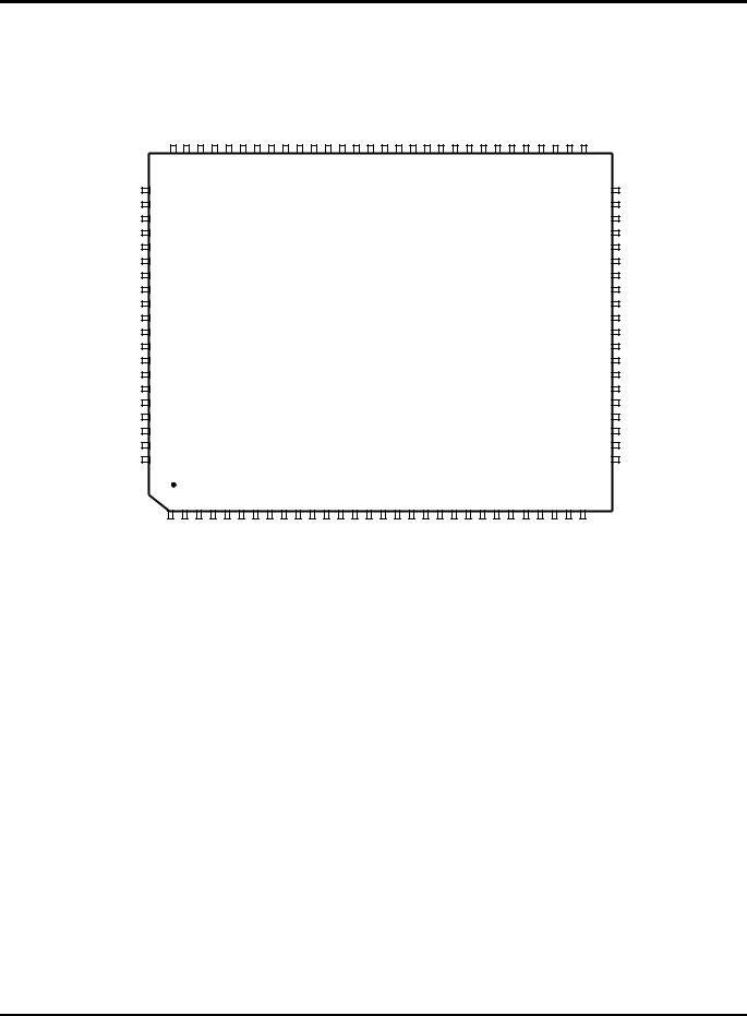
Figure 4. Z89139 100-Pin QFP Pin Configuration
8 |
P R E L I M I N A R Y |
DS97TAD0201 |

|
|
|
Z89138/Z89139 |
|
Zilog |
|
|
Voice Processing Controllers |
|
|
|
|
||
|
Table 3. Z89139 100-Pin QFP Pin Identification |
|||
|
|
|
|
|
I/O Port |
|
|
|
|
Symbol |
Pin Number |
Direction |
Function |
|
|
|
|
|
|
GND |
3, 53, 88, 97 |
|
Digital Ground |
|
|
|
|
|
|
VCC |
5, 16, 47, 77 |
|
Digital VCC = +5V |
|
VREF+ |
1 |
Input/Output |
Analog Voltage Ref+ |
|
|
|
|
|
|
ANVDD |
2 |
|
Analog VDD |
|
PWM |
4 |
Output |
PWM Output |
|
|
|
|
|
|
DSP1-0 |
6, 7 |
Output |
DSP User Output 1, 0 |
|
|
|
|
|
|
/AS |
8 |
Output |
Address Strobe |
|
|
|
|
|
|
/DS |
9 |
Output |
Data Strobe |
|
|
|
|
|
|
R//W |
10 |
Output |
Read/Write |
|
|
|
|
|
|
NC |
11 |
|
No Connection |
|
|
|
|
|
|
P57-P54 |
12-15 |
Input/Output |
Port 5 Bit 7-4 |
|
|
|
|
|
|
XTAL2 |
17 |
Output |
Crystal Output (20.48 or 29.49 MHz) |
|
|
|
|
|
|
XTAL1 |
18 |
Input |
Crystal Input (20.48 or 29.49 MHz) |
|
|
|
|
|
|
P53-P52 |
19, 20 |
Input/Output |
Port 5 Bit 3-2 |
|
|
|
|
|
|
P37-P34 |
21-24 |
Output |
Port 3 Bit 7-4 |
|
|
|
|
|
|
P33-P31 |
25-27 |
Input |
Port 3 Bit 3-1 |
|
|
|
|
|
|
/RESET |
28 |
Input/Output |
Reset |
|
|
|
|
|
|
P20-P27 |
29-36 |
Input/Output |
Port 2, Bit 0-7 |
|
|
|
|
|
|
P40-P47 |
37-44 |
Input/Output |
Port 4, Bit 0-7 |
|
|
|
|
|
|
P50-P51 |
45, 46 |
Input/Output |
Port 5, Bit 0-1 |
|
|
|
|
|
|
NC |
48-52 |
|
No Connection |
|
|
|
|
|
|
OSC1 |
54 |
Input |
Crystal Input (32.768 kHz) |
|
|
|
|
|
|
OSC2 |
55 |
Output |
Crystal Output (32.768 kHz) |
|
|
|
|
|
|
NC |
56-76 |
|
No Connection |
|
|
|
|
|
|
NC |
78-79 |
|
No Connection |
|
|
|
|
|
|
P07-P00 |
80-87 |
Input/Output |
Port 0, Bit 7-0 |
|
|
|
|
|
|
P17-P10 |
89-96 |
Input/Output |
Port 1, Bit 7-0 |
|
|
|
|
|
|
ANGND |
98 |
|
Analog GND |
|
|
|
|
|
|
VREF- |
99 |
Input |
Analog Voltage Ref- |
|
|
|
|
|
|
ANIN |
100 |
Input |
Analog Input |
|
|
|
|
|
|
DS97TAD0201 |
P R E L I M I N A R Y |
9 |
Z89138/Z89139 |
|
Voice Processing Controllers |
Zilog |
PIN DESCRIPTION (Continued)
|
VCC NC NC NC NC NC NC NC NC NC NC NC NC NC NC NC NC NC |
NC NC NC NC OSC2 OSC1 GND |
||||
|
75 |
70 |
65 |
60 |
55 |
51 |
NC |
76 |
|
|
|
|
50 |
NC |
|
|
|
|
|
|
P07 |
|
|
|
|
|
|
P06 |
|
|
|
|
|
|
P05 |
80 |
|
|
|
|
|
P04 |
|
|
|
|
|
45 |
P03 |
|
|
|
|
|
|
P02 |
|
|
|
|
|
|
P01 |
|
|
|
|
|
|
P00 |
85 |
|
|
|
|
|
GND |
|
|
|
|
40 |
|
|
|
|
|
|
||
P17 |
|
|
100-Pin VQFP |
|
|
|
P16 |
|
|
|
|
||
|
|
|
|
|
|
|
P15 |
|
|
|
|
|
|
P14 |
|
|
|
|
|
|
P13 |
90 |
|
|
|
|
35 |
P12 |
|
|
|
|
|
|
P11 |
|
|
|
|
|
|
P10 |
|
|
|
|
|
|
GND |
|
|
|
|
|
|
AGND |
95 |
|
|
|
|
30 |
VREF- |
|
|
|
|
|
|
|
|
|
|
|
|
|
ANIN |
|
|
|
|
|
|
VREF+ |
100 |
|
|
|
|
|
ANVDD |
|
|
|
|
26 |
|
|
1 |
5 |
10 |
15 |
20 |
25 |
|
GND PWM VCC DSP1 |
DSP0 /AS |
/DS R//W NC P57 P56 |
P55 P54 VCC XTAL2 XTAL1 P53 P52 |
P37 P36 P35 P34 P33 |
P32 P31 |
Figure 5. Z89139 100-Pin VQFP Pin Configuration
NC
NC
NC
NC
NC
VCC
P51
P50
P47
P46
P45
P44
P43
P42
P41
P40
P27
P26
P25
P24
P23
P22
P21
P20
/RESET
10 |
P R E L I M I N A R Y |
DS97TAD0201 |
|
|
|
Z89138/Z89139 |
|
Zilog |
|
|
Voice Processing Controllers |
|
|
|
|
||
|
Table 4. Z89139 100-Pin VQFP Pin Identification |
|||
|
|
|
|
|
I/O Port |
|
|
|
|
Symbol |
Pin Number |
Direction |
Function |
|
|
|
|
|
|
GND |
1, 51, 86, 95 |
|
Digital Ground |
|
|
|
|
|
|
VCC |
3, 14, 45, 75 |
|
Digital VCC = +5V |
|
VREF+ |
99 |
Input/Output |
Analog Voltage Ref+ |
|
|
|
|
|
|
ANVDD |
100 |
|
Analog VDD |
|
PWM |
2 |
Output |
PWM Output |
|
|
|
|
|
|
DSP1-0 |
4, 5 |
Output |
DSP User Output 1, 0 |
|
|
|
|
|
|
/AS |
6 |
Output |
Address Strobe |
|
|
|
|
|
|
/DS |
7 |
Output |
Data Strobe |
|
|
|
|
|
|
R//W |
8 |
Output |
Read/Write |
|
|
|
|
|
|
NC |
9 |
|
No Connection |
|
|
|
|
|
|
P57-P54 |
10-13 |
Input/Output |
Port 5 Bit 7-4 |
|
|
|
|
|
|
XTAL2 |
15 |
Output |
Crystal Output (20.48 or 29.49 MHz) |
|
|
|
|
|
|
XTAL1 |
16 |
Input |
Crystal Input (20.48 or 29.49 MHz) |
|
|
|
|
|
|
P53-P52 |
17, 18 |
Input/Output |
Port 5 Bit 3-2 |
|
|
|
|
|
|
P37-P34 |
19-22 |
Output |
Port 3 Bit 7-4 |
|
|
|
|
|
|
P33-P31 |
23-25 |
Input |
Port 3 Bit 3-1 |
|
|
|
|
|
|
/RESET |
26 |
Input/Output |
Reset |
|
|
|
|
|
|
P20-P27 |
27-34 |
Input/Output |
Port 2, Bit 0-7 |
|
|
|
|
|
|
P40-P47 |
35-42 |
Input/Output |
Port 4, Bit 0-7 |
|
|
|
|
|
|
P50-P51 |
43, 44 |
Input/Output |
Port 5, Bit 0-1 |
|
|
|
|
|
|
NC |
46-50 |
|
No Connection |
|
|
|
|
|
|
OSC1 |
52 |
Input |
Crystal Input (32.768 kHz) |
|
|
|
|
|
|
OSC2 |
53 |
Output |
Crystal Output (32.768 kHz) |
|
|
|
|
|
|
NC |
54-74 |
|
No Connection |
|
|
|
|
|
|
NC |
76, 77 |
|
No Connection |
|
|
|
|
|
|
P07-P00 |
78-85 |
Input/Output |
Port 0, Bit 7-0 |
|
|
|
|
|
|
P17-P10 |
87-94 |
Input/Output |
Port 1, Bit 7-0 |
|
|
|
|
|
|
ANGND |
96 |
|
Analog GND |
|
|
|
|
|
|
VREF- |
97 |
Input |
Analog Voltage Ref- |
|
|
|
|
|
|
ANIN |
98 |
Input |
Analog Input |
|
|
|
|
|
|
DS97TAD0201 |
P R E L I M I N A R Y |
11 |
Z89138/Z89139 |
|
Voice Processing Controllers |
Zilog |
ABSOLUTE MAXIMUM RATINGS
Sym |
Description |
Min |
Max |
Units |
|
|
|
|
|
VCC |
Supply |
–0.3 |
+7.0 |
V |
|
Voltage (*) |
|
|
|
|
|
|
|
|
TSTG |
Storage Temp |
–65° |
+150° |
C |
TA |
Oper. |
|
† |
C |
Ambient
Temp.
Notes:
*Voltage on all pins with respect to GND. †See Ordering Information.
Stresses greater than those listed under Absolute Maximum Ratings can cause permanent damage to the device. This is a stress rating only; operation of the device at any condition above those indicated in the operational sections of these specifications is not implied. Exposure to absolute maximum rating conditions for an extended period can affect device reliability.
STANDARD TEST CONDITIONS
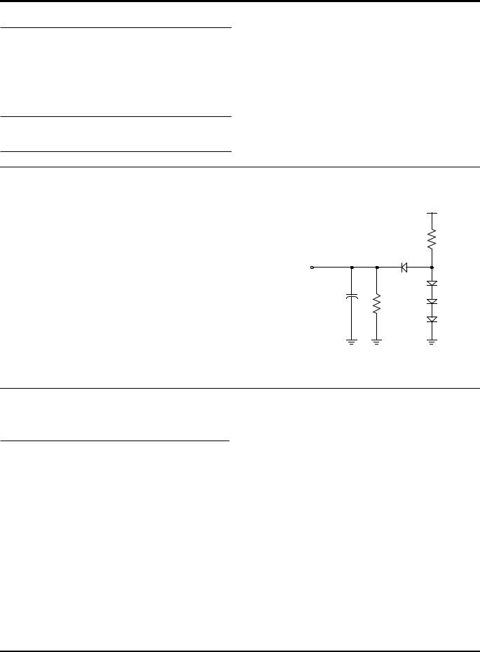
The characteristics listed below apply for standard test conditions as noted. All voltages are referenced to GND. Positive current flows into the referenced pin (Figure 6).
+5V
2.1 kΩ
From Output
Under Test
150 pF
9.1 kΩ
Figure 6. Test Load Diagram
CAPACITANCE
TA = 25°C, VCC = GND = 0V, f = 1.0 MHz, unmeasured pins returned to GND.
Parameter |
Min |
Max |
|
|
|
Input capacitance |
0 |
12 pF |
|
|
|
Output capacitance |
0 |
12 pF |
|
|
|
I/O capacitance |
0 |
12 pF |
|
|
|
12 |
P R E L I M I N A R Y |
DS97TAD0201 |

|
|
|
|
|
|
|
Z89138/Z89139 |
|
Zilog |
|
|
|
|
|
Voice Processing Controllers |
||
|
|
|
|
|
|
|
||
DC ELECTRICAL CHARACTERISTICS |
|
|
|
|
|
|
||
|
|
|
|
|
|
|
|
|
|
|
VCC |
TA = 0°C to +55°C |
Typical |
|
|
|
|
Sym |
Parameter |
Note 1 |
Min |
Max |
@ 25°C |
Units |
Conditions |
|
|
|
|
|
|
|
|
|
|
ICC |
Supply Current |
5.0V |
|
65 |
40 |
mA |
|
|
ICC1 |
Halt Mode Current |
5.0V |
|
20 |
6 |
mA |
|
|
ICC2 |
Stop Mode Current |
5.0V |
|
20 |
6 |
A |
See Note 2 |
|
VMAX |
Max Input Voltage |
5.0V |
|
7 |
|
|
|
|
VCH |
Clock Input High |
5.0V |
0.9 VCC |
VCC +0.3 |
2.5 |
V |
Driven by External |
|
|
Voltage |
|
|
|
|
|
Clock Generator |
|
VCL |
Clock Input Low |
5.0V |
GND –0.3 |
0.1 VCC |
1.5 |
V |
Driven by External |
|
|
Voltage |
|
|
|
|
|
Clock Generator |
|
|
|
|
|
|
|
|
|
|
VIH |
Input High Voltage |
5.0V |
0.7 VCC |
VCC +0.3 |
2.5 |
V |
|
|
VIL |
Input Low Voltage |
5.0V |
GND –0.3 |
0.2 VCC |
1.5 |
V |
|
|
VOH |
Output High Voltage |
5.0V |
VCC–0.4 |
|
4.8 |
V IOH = –2.0 mA |
|
|
VOL1 |
Output Low Voltage |
5.0V |
|
0.4 |
0.1 |
V |
IOL = +4.0 mA |
|
VOL2 |
Output Low Voltage |
5.0V |
|
1.2 |
0.3 |
V IOL = +12 mA, 3 Pin |
||
|
|
|
|
|
|
|
Max |
|
|
|
|
|
|
|
|
|
|
VRH |
Reset Input High |
5.0V |
.8 VCC |
VCC |
2.1 |
V |
|
|
|
Voltage |
|
|
|
|
|
|
|
|
|
|
|
|
|
|
|
|
VRl |
Reset Input Low |
5.0V |
GND –0.3 |
|
0.2 VCC |
1.7 |
|
|
|
Voltage |
|
|
|
|
|
|
|
|
|
|
|
|
|
|
|
|
VOFFSET |
Comparator Input |
5.0V |
|
|
25 |
10 |
mV |
|
|
Offset |
|
|
|
|
|
|
|
|
|
|
|
|
|
|
|
|
|
Voltage |
|
|
|
|
|
|
|
|
|
|
|
|
|
|
|
|
IIL |
Input Leakage |
5.0V |
–10 |
|
10 |
10 |
A |
|
IOL |
Output Leakage |
5.0V |
–10 |
|
10 |
10 |
A |
|
IIR |
Reset Input Current |
5.0V |
|
|
–55 |
–30 |
A |
|
Notes:
1.5.0V ±0.5V
2.When a 32 kHz crystal is used, additional value must be added to the STOP Mode current ICC2. The sum will be 200 A/max, 150 A/typical.
DS97TAD0201 |
P R E L I M I N A R Y |
13 |

Z89138/Z89139 |
|
Voice Processing Controllers |
Zilog |
DC ELECTRICAL CHARACTERISTICS
Z89138 A/D Converter
|
|
|
TA = 0° C to +55°C |
|
|
|
|
|
|
Sym |
Parameter |
VDD |
Min |
Max |
Units |
|
Conditions |
|
|
IIL |
Input Leakage |
5.5V |
|
1.00 |
A |
ANVDD |
= |
5.50 |
V |
|
Analog Input |
|
|
|
|
|
|
|
|
|
|
|
|
|
|
|
|
|
|
|
|
|
|
|
|
VIN |
= |
0.00 |
V |
|
|
|
|
|
|
VREFH |
= |
5.50 |
V |
|
|
|
|
|
|
VREFL |
= |
0.00 |
V |
IIH |
Input Leakage |
5.5V |
|
2.00 |
A |
ANVDD |
= |
5.50 |
V |
|
Analog Input |
|
|
|
|
|
|
|
|
|
|
|
|
|
|
|
|
|
|
|
|
|
|
|
|
VIN |
= |
5.50 |
V |
|
|
|
|
|
|
VREFH |
= |
5.50 |
V |
|
|
|
|
|
|
VREFL |
= |
0.00 |
V |
IVREFH |
Input Current |
5.5V |
|
1.00 |
mA |
VIN |
= |
5.50 |
V |
|
|
|
|
|
|
VREFL |
= |
0.00 |
V |
|
|
|
|
|
|
ANVDD |
= |
5.50 |
V |
IVREFL |
Input Current |
5.5V |
|
2 |
A |
VIN |
= |
5.50 |
V |
|
|
|
|
|
|
VREFL |
= |
5.50 |
V |
|
|
|
|
|
|
ANVDD |
= |
5.50 |
V |
IVEFL |
Input Current |
5.5V |
|
–2.00 |
mA |
VIN |
= |
0.00 |
V |
|
|
|
|
|
|
VREFH |
= |
5.50 |
V |
|
|
|
|
|
|
ANVDD |
= |
0.00 |
V |
IVREFL |
Input Current |
5.5V |
|
2 |
A |
VIN |
= |
0.00 |
V |
|
|
|
|
|
|
VREFH |
= |
5.50 |
V |
|
|
|
|
|
|
ANVDD |
= |
5.50 |
V |
14 |
P R E L I M I N A R Y |
DS97TAD0201 |

|
Z89138/Z89139 |
Zilog |
Voice Processing Controllers |
|
|
DC ELECTRICAL CHARACTERISTICS
21 Other Non-Regular I/O
|
|
|
TA = 0° C to +55°C |
|
|
|
Sym |
Parameter |
VDD |
Min |
Max |
Units |
Conditions |
IIRH |
Input Current ROMless Pin |
5.5V |
|
6.00 |
A |
VIN = 5.50 V |
IIR1 |
Input Current ROMless Pin |
5.5V |
|
6.00 |
A |
VIN = 0.00 V |
IIR |
Input Current ROMless Pin |
5.5V |
|
1.00 |
mA |
VIN = 5.50 V |
|
During Reset Active |
|
|
|
|
|
|
|
|
|
|
|
|
IIHX2 |
Input Current |
5.5V |
|
1.00 |
A |
VIN = 0.00 V |
|
XTAL2 pin in STOP Mode |
|
|
|
|
|
|
|
|
|
|
|
|
IILX2 |
Input Current |
5.5V |
|
1.00 |
A |
VIN = 5.50 V |
|
XTAL2 Pin in STOP Mode |
|
|
|
|
|
IIHX1 |
Input current |
5.5V |
|
30 |
A |
VIN = 0.00 V |
|
XTAL1 Pin |
|
|
|
|
|
|
|
|
|
|
|
|
IILX1 |
Input Current |
5.5V |
|
30 |
A |
VIN = 5.50 V |
|
XTAL1 Pin |
|
|
|
|
|
|
|
|
|
|
|
|
VOLXR |
Output Low |
5.5V |
|
1.20 |
V |
IOL = 4.00 mA |
|
Voltage XTAL2 Reset Inactive |
|
|
|
|
|
VOLX |
Output Low |
5.5V |
|
0.60 |
V |
IOL =1.00 mA |
|
Voltage XTAL2 Reset Inactive |
|
|
|
|
|
VOHXR |
Output High |
5.5V |
4.00 |
|
V |
IOH = 4.00 mA |
|
Voltage XTAL2 Reset Inactive |
|
|
|
|
|
|
|
|
|
|
|
|
IVOHX |
Output High |
5.5V |
4.00 |
|
V |
IOH =1.00 mA |
|
Voltage XTAL2 Reset Inactive |
|
|
|
|
|
|
|
|
|
|
|
|
IIH |
Input Current |
5.5V |
|
1.00 |
A |
VIN = 5.50 V |
|
P31, P32, P33 |
|
|
|
|
|
IIL |
Input Current |
5.5V |
|
1.00 |
A |
VIN = 0.00 V |
|
P31, P32, P33 |
|
|
|
|
|
DS97TAD0201 |
P R E L I M I N A R Y |
15 |

Z89138/Z89139 |
|
Voice Processing Controllers |
Zilog |
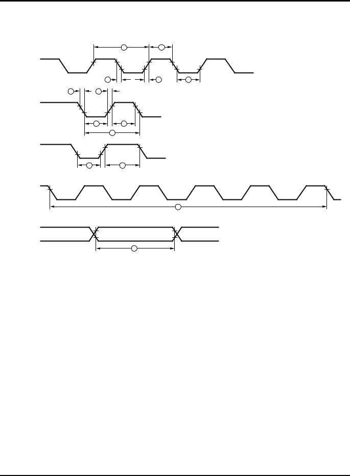
AC CHARACTERISTICS
External I/O or Memory Read and Write Timing Diagram
R//W |
|
|
|
|
|
|
|
|
13 |
12 |
|
|
|
|
Port 0, /DM |
|
|
|
|
|
16 |
|
|
|
19 |
3 |
|
|
|
Port 1 |
A7 - A0 |
|
D7 - D0 IN |
|
1 |
2 |
|
|
9 |
/AS |
|
|
|
|
|
8 |
|
18 |
11 |
4 |
|
|
|
|
|
5 |
6 |
|
|
/DS |
|
|
|
|
(Read) |
17 |
|
|
|
|
|
|
|
10 |
Port1 |
A7 - A0 |
D7 - D0 |
OUT |
|
|
14 |
|
|
15 |
|
|
|
7 |
|
/DS |
|
|
|
|
(Write) |
|
|
|
|
Figure 7. External I/O or Memory Read/Write Timing
16 |
P R E L I M I N A R Y |
DS97TAD0201 |

|
Z89138/Z89139 |
Zilog |
Voice Processing Controllers |
|
|
AC CHARACTERISTICS
External I/O or Memory Read and Write Timing Table
|
|
|
VCC |
TA= 0°C to +55°C |
|
|
|
No |
Symbol |
Parameter |
Note [4] |
Min |
Max |
Units |
Notes |
|
|
|
|
|
|
|
|
1 |
TdA(AS) |
Address Valid to /AS Rise Delay |
5.0V |
25 |
|
ns |
2,3 |
|
|
|
|
|
|
|
|
2 |
TdAS(A) |
/AS Rise to Address Float Delay |
5.0V |
35 |
|
ns |
2,3 |
|
|
|
|
|
|
|
|
3 |
TdAS(DR) |
/AS Rise to Read Data Req’d Valid |
5.0V |
|
150 |
ns |
1,2,3 |
|
|
|
|
|
|
|
|
4 |
TwAS |
/AS Low Width |
5.0V |
35 |
|
ns |
2,3 |
|
|
|
|
|
|
|
|
5 |
TdAZ(DS) |
Address Float to /DS Fall |
5.0V |
0 |
|
ns |
|
|
|
|
|
|
|
|
|
6 |
TwDSR |
/DS (Read) Low Width |
5.0V |
125 |
|
ns |
1,2,3 |
|
|
|
|
|
|
|
|
7 |
TwDSW |
/DS (Write) Low Width |
5.0V |
75 |
|
ns |
1,2,3 |
|
|
|
|
|
|
|
|
8 |
TdDSR(DR) |
/DS Fall to Read Data Req’d Valid |
5.0V |
|
90 |
ns |
1,2,3 |
|
|
|
|
|
|
|
|
9 |
ThDR(DS) |
Read Data to /DS Rise Hold Time |
5.0V |
0 |
|
ns |
2,3 |
|
|
|
|
|
|
|
|
10 |
TdDS(A) |
/DS Rise to Address Active Delay |
5.0V |
40 |
|
ns |
2,3 |
|
|
|
|
|
|
|
|
11 |
TdDS(AS) |
/DS Rise to /AS Fall Delay |
5.0V |
35 |
|
ns |
2,3 |
|
|
|
|
|
|
|
|
12 |
TdR/W(AS) |
R//W Valid to /AS Rise Delay |
5.0V |
25 |
|
ns |
2,3 |
|
|
|
|
|
|
|
|
13 |
TdDS(R/W) |
/DS Rise to R//W Not Valid |
5.0V |
35 |
|
ns |
2,3 |
|
|
|
|
|
|
|
|
14 |
TdDW(DSW) |
Write Data Valid to /DS Fall (Write) Delay |
5.0V |
40 |
|
ns |
2,3 |
|
|
|
|
|
|
|
|
15 |
TdDS(DW) |
/DS Rise to Write Data Not Valid Delay |
5.0V |
25 |
|
ns |
2,3 |
|
|
|
|
|
|
|
|
16 |
TdA(DR) |
Address Valid to Read Data Req’d Valid |
5.0V |
|
180 |
ns |
1,2,3 |
|
|
|
|
|
|
|
|
17 |
TdAS(DS) |
/AS Rise to /DS Fall Delay |
5.0V |
48 |
|
ns |
2,3 |
|
|
|
|
|
|
|
|
18 |
TdDI(DS) |
Data Input Setup to /DS Rise |
5.0V |
50 |
|
ns |
1,2,3 |
|
|
|
|
|
|
|
|
19 |
TdDM(AS) |
/DM Valid to /AS Fall Delay |
5.0V |
20 |
|
ns |
2,3 |
|
|
|
|
|
|
|
|
Notes:
1.When using extended memory timing add 2 TpC.
2.Timing numbers given are for minimum TpC.
3.See clock cycle dependent characteristics table.
4.5.0V ±0.5 V.
Standard Test Load
All timing references use 0.9 VCC for a logic 1 and 0.1 VCC for a logic 0.
DS97TAD0201 |
P R E L I M I N A R Y |
17 |
Z89138/Z89139 |
|
Voice Processing Controllers |
Zilog |
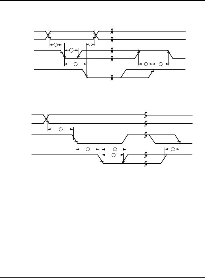
AC ELECTRICAL CHARACTERISTICS
Additional Timing Diagram
1 |
3 |
Clock
2 |
2 |
3 |
7 |
7 |
TIN |
|
4 |
5 |
|
6 |
IRQN |
|
8 |
9 |
Clock
Setup
11
Stop
Mode
Recovery
Source
10
Figure 8. Additional Timing
18 |
P R E L I M I N A R Y |
DS97TAD0201 |

|
Z89138/Z89139 |
Zilog |
Voice Processing Controllers |
|
|
AC ELECTRICAL CHARACTERISTICS
Additional Timing Table
|
|
|
VCC |
TA= 0°C to +55°C |
|
|
|
No |
Sym |
Parameter |
Note 5 |
Min |
Max |
Units |
Notes |
|
|
|
|
|
|
|
|
1 |
TpC |
Input Clock Period |
5.0V |
48.83 |
|
ns |
1, 6 |
|
|
|
|
|
|
|
|
2 |
TrC,TfC |
Clock Input Rise & Fall Times |
5.0V |
|
6 |
ns |
1 |
|
|
|
|
|
|
|
|
3 |
TwC |
Input Clock Width |
5.0V |
17 |
|
ns |
1,7 |
|
|
|
|
|
|
|
|
4 |
TwTinL |
Timer Input Low Width |
5.0V |
70 |
|
ns |
|
|
|
|
|
|
|
|
|
5 |
TwTinH |
Timer Input High Width |
5.0V |
3TpC |
|
|
1 |
|
|
|
|
|
|
|
|
6 |
TpTin |
Timer Input Period |
5.0V |
8TpC |
|
|
1 |
|
|
|
|
|
|
|
|
7 |
TrTin, TfTin |
Timer Input Rise & Fall Timer |
5.0V |
|
100 |
ns |
1 |
|
|
|
|
|
|
|
|
8a |
TwIL |
Int. Request Low Time |
5.0V |
70 |
|
ns |
1,2 |
|
|
|
|
|
|
|
|
8b |
TwIL |
Int. Request Low Time |
5.0V |
3TpC |
|
|
1 |
|
|
|
|
|
|
|
|
9 |
TwIH |
Int. Request Input High Time |
5.0V |
3TpC |
|
|
1 |
|
|
|
|
|
|
|
|
10 |
Twsm |
Stop-Mode Recovery Width Spec |
5.0V |
12 |
|
ns |
1 |
|
|
|
|
|
|
|
|
11 |
Tost |
Oscillator Start-up Time |
5.0V |
5TpC |
|
|
3 |
|
|
|
|
|
|
|
|
12 |
Twdt |
Watch-Dog Timer |
5.0V |
5 |
|
ms |
D1 = 0, D0 = 0 [4] |
|
|
|
|
|
|
|
|
|
|
|
5.0V |
15 |
|
ms |
D1 = 0, D0 = 1 [4] |
|
|
|
|
|
|
|
|
|
|
|
5.0V |
25 |
|
ms |
D1 = 1, D0 = 0 [4] |
|
|
|
|
|
|
|
|
|
|
|
5.0V |
100 |
|
ms |
D1 = 1, D0 = 1 [4] |
|
|
|
|
|
|
|
|
Notes:
1.Timing Reference uses 0.9 VCC for a logic 1 and 0.1 VCC for a logic 0.
2.Interrupt request via Port 3 (P31-P33).
3.SMR-D5 = 0
4.Reg. WDT
5.5.0V ±0.5 V
6.For 29.49 MHz, it will be 30.53 ns.
7.For 29.49 MHz, it will be 9 ns.
DS97TAD0201 |
P R E L I M I N A R Y |
19 |
Z89138/Z89139 |
|
Voice Processing Controllers |
Zilog |
AC ELECTRICAL CHARACTERISTICS
Handshake Timing Diagrams
Data In |
Data In Valid |
Next Data In Valid |
|
1 |
2 |
3 |
|
|
/DAV |
Delayed DAV |
|
(Input) |
|
|
4 |
5 |
6 |
RDY |
Delayed RDY |
|
(Output) |
|
|
Figure 9. Input Handshake Timing
Data Out |
Data Out Valid |
|
Next Data Out Valid |
|
7 |
|
|
/DAV |
|
|
Delayed DAV |
(Output) |
|
|
|
|
8 |
9 |
11 |
|
|
10 |
|
RDY |
|
|
Delayed RDY |
(Input) |
|
|
|
Figure 10. Output Handshake Timing
20 |
P R E L I M I N A R Y |
DS97TAD0201 |
 Loading...