


Z86E0812PEC
ZILOG Z86E0812PEC, Z86E0812PSC1860, Z86E0812PSC1866, Z86E0812PSC1903, Z86E0812PSC1924 Datasheet
...
DS97Z8X0401
P R E L I M I N A R Y
1
1
P
RELIMINARY
P
RODUCT
S
PECIFICATION
Z86E04/E08
1
CMOS Z8 OTP M
ICROCONTROLLERS
PRODUCT DEVICES
Several key product features of the extensive family of Zilog Z86E04/E08 CMOS OTP microcontrollers are presented in
the above table. This table enables the user to identify which of the twenty E04/E08 product variants most closely match
the user’s application requirements.
Part Oscillator Operating Operating ROM
Number Type
V
CC
Temperature (KB) Package
Z86E0412PEC Crystal 4.5V - 5.5V -40
°
C/105
°
C 1 18-Pin DIP
Z86E0412PSC1860 Crystal 3.0V - 5.5V 0
°
C/70
°
C 1 18-Pin DIP
Z86E0412PSC1866 Crystal 4.5V - 5.5V 0
°
C/70
°
C 1 18-Pin DIP
Z86E0412PSC1903 RC 4.5V - 5.5V 0
°
C/70
°
C 1 18-Pin DIP
Z86E0412PSC1924 RC 3.0V - 5.5V 0
°
C/70
°
C 1 18-Pin DIP
Z86E0412SEC Crystal 4.5V - 5.5V -40
°
C/105
°
C 1 18-Pin SOIC
Z86E0412SSC1860 Crystal 3.0V - 5.5V 0
°
C/70
°
C 1 18-Pin SOIC
Z86E0412SSC1866 Crystal 4.5V - 5.5V 0
°
C/70
°
C 1 18-Pin SOIC
Z86E0412SSC1903 RC 4.5V - 5.5V 0
°
C/70
°
C 1 18-Pin SOIC
Z86E0412SSC1924 RC 3.0V - 5.5V 0
°
C/70
°
C 1 18-Pin SOIC
Z86E0812PEC Crystal 4.5V - 5.5V -40
°
C/105
°
C 2 18-Pin DIP
Z86E0812PSC1860 Crystal 3.0V - 5.5V 0
°
C/70
°
C 2 18-Pin DIP
Z86E0812PSC1866 Crystal 4.5V - 5.5V 0
°
C/70
°
C 2 18-Pin DIP
Z86E0812PSC1903 RC 4.5V - 5.5V 0
°
C/70
°
C 2 18-Pin DIP
Z86E0812PSC1924 RC 3.0V - 5.5V 0
°
C/70
°
C 2 18-Pin DIP
Z86E0812SEC Crystal 4.5V - 5.5V -40
°
C/105
°
C 2 18-Pin SOIC
Z86E0812SSC1860 Crystal 3.0V - 5.5V 0
°
C/70
°
C 2 18-Pin SOIC
Z86E0812SSC1866 Crystal 4.5V - 5.5V 0
°
C/70
°
C 2 18-Pin SOIC
Z86E0812SSC1903 RC 4.5V - 5.5V 0
°
C/70
°
C 2 18-Pin SOIC
Z86E0812SSC1924 RC 3.0V - 5.5V 0
°
C/70
°
C 2 18-Pin SOIC

Z86E04/E08
CMOS Z8 OTP Microcontrollers Zilog
2
P R E L I M I N A R Y
DS97Z8X0401
FEATURES
■
14 Input / Output Lines
■
Six Vectored, Prioritized Interrupts
(3 falling edge, 1 rising edge, 2 timers)
■
Two Analog Comparators
■
Program Options:
– Low Noise
– ROM Protect
– Auto Latch
– Watch-Dog Timer (WDT)
– EPROM/Test Mode Disable
■
Two Programmable 8-Bit Counter/Timers, Each with
6-Bit Programmable Prescaler
■
WDT/ Power-On Reset (POR)
■
On-Chip Oscillator that Accepts XTAL, Ceramic
Resonance, LC, RC, or External Clock
■
Clock-Free WDT Reset
■
Low-Power Consumption (50 mw typical)
■
Fast Instruction Pointer (1
µ
s @ 12 MHz)
■
RAM Bytes (125)
GENERAL DESCRIPTION
Zilog's Z86E04/E08 Microcontrollers (MCU) are One-Time
Programmable (OTP) members of Zilog’s single-chip Z8
®
MCU family that allow easy software development, debug,
prototyping, and small production runs not economically
desirable with masked ROM versions.
For applications demanding powerful I/O capabilities, the
Z86E04/E08's dedicated input and output lines are
grouped into three ports, and are configurable under soft-
ware control to provide timing, status signals, or parallel
I/O.
Two on-chip counter/timers, with a large number of user
selectable modes, offload the system of administering
real-time tasks such as counting/timing and I/O data com-
munications.
Note:
All Signals with a preceding front slash, “/”, are
active Low, for example: B//W (WORD is active Low); /B/W
(BYTE is active Low, only).
Power connections follow conventional descriptions be-
low:
Connection Circuit Device
Power
V
CC
V
DD
Ground GND
V
SS
Z86E04/E08
Zilog CMOS Z8 OTP Microcontrollers
DS97Z8X0401
P R E L I M I N A R Y
3
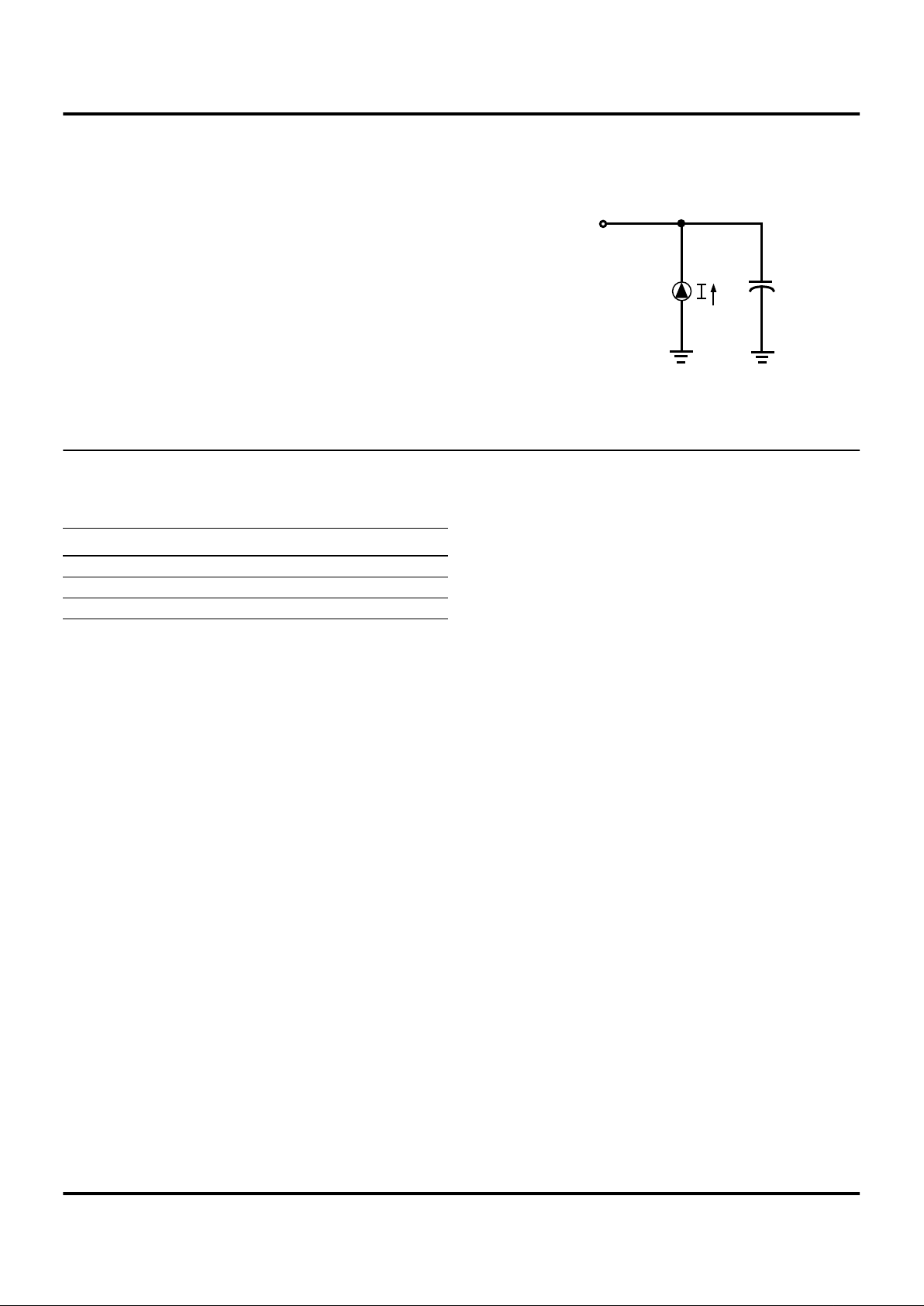
1
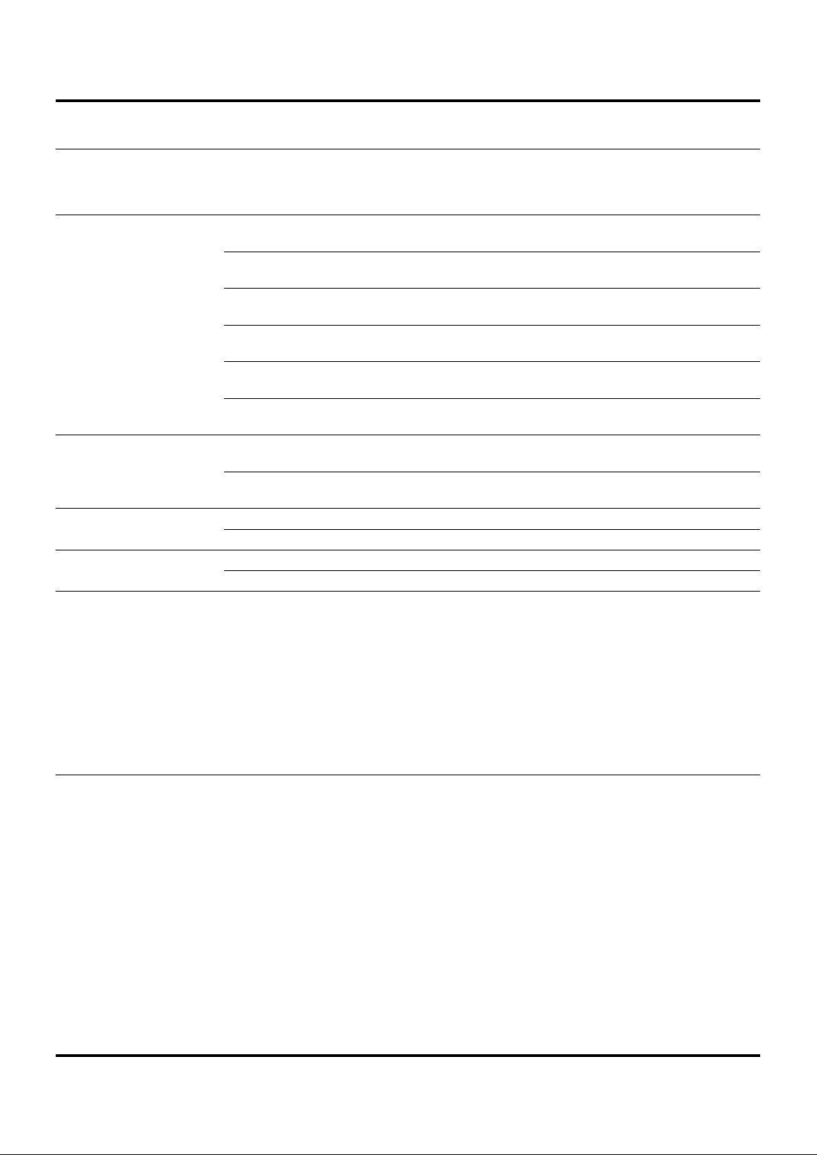
Figure 1. Functional Block Diagram
Port 3
Counter/
Timers (2)
Interrupt
Control
T wo Analog
Comparators
Port 2
I/O
(Bit Programmable)
FLAG
Register
Pointer
General-Purpose
Register File
Machine
Timing & Inst.
Control
OTP
Program
Counter
Vcc GND
XTAL
Port 0
I/O
Input
ALU
Z86E04/E08
CMOS Z8 OTP Microcontrollers Zilog
4
P R E L I M I N A R Y
DS97Z8X0401
GENERAL DESCRIPTION
(Continued)
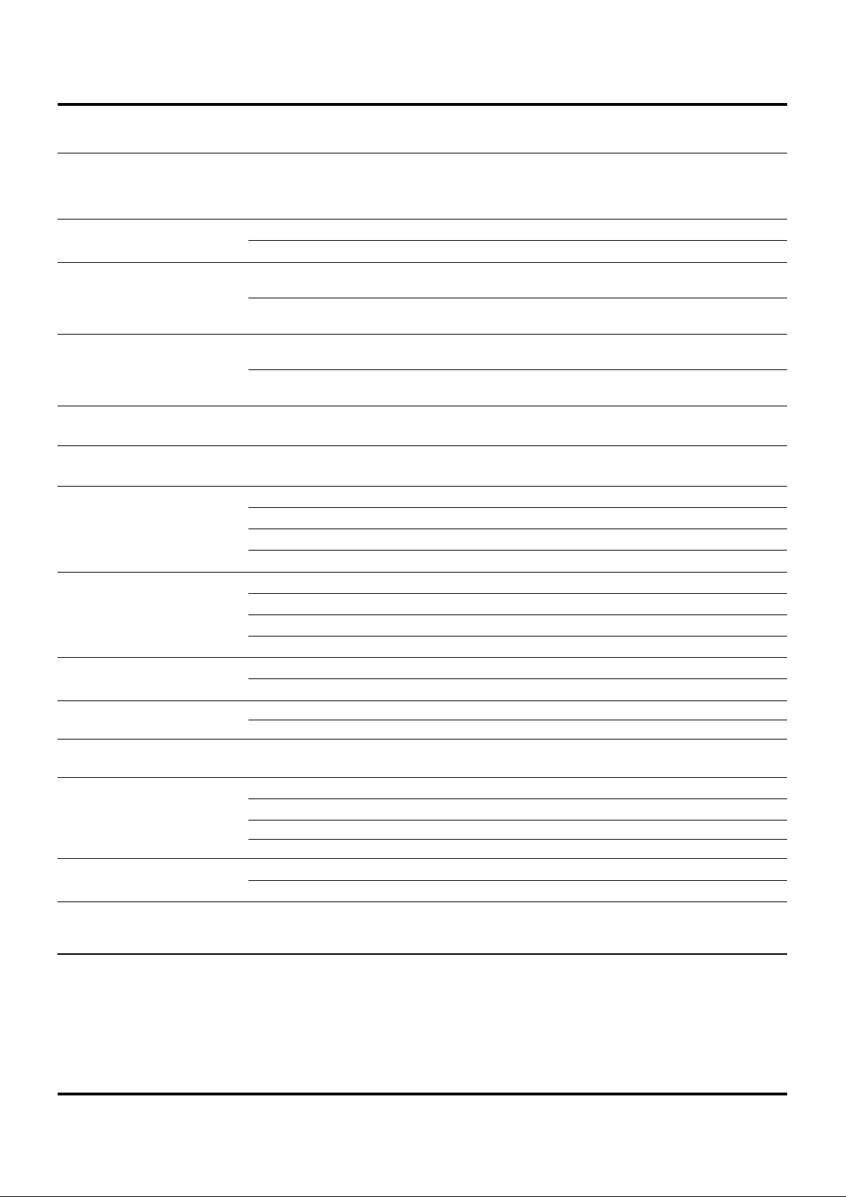
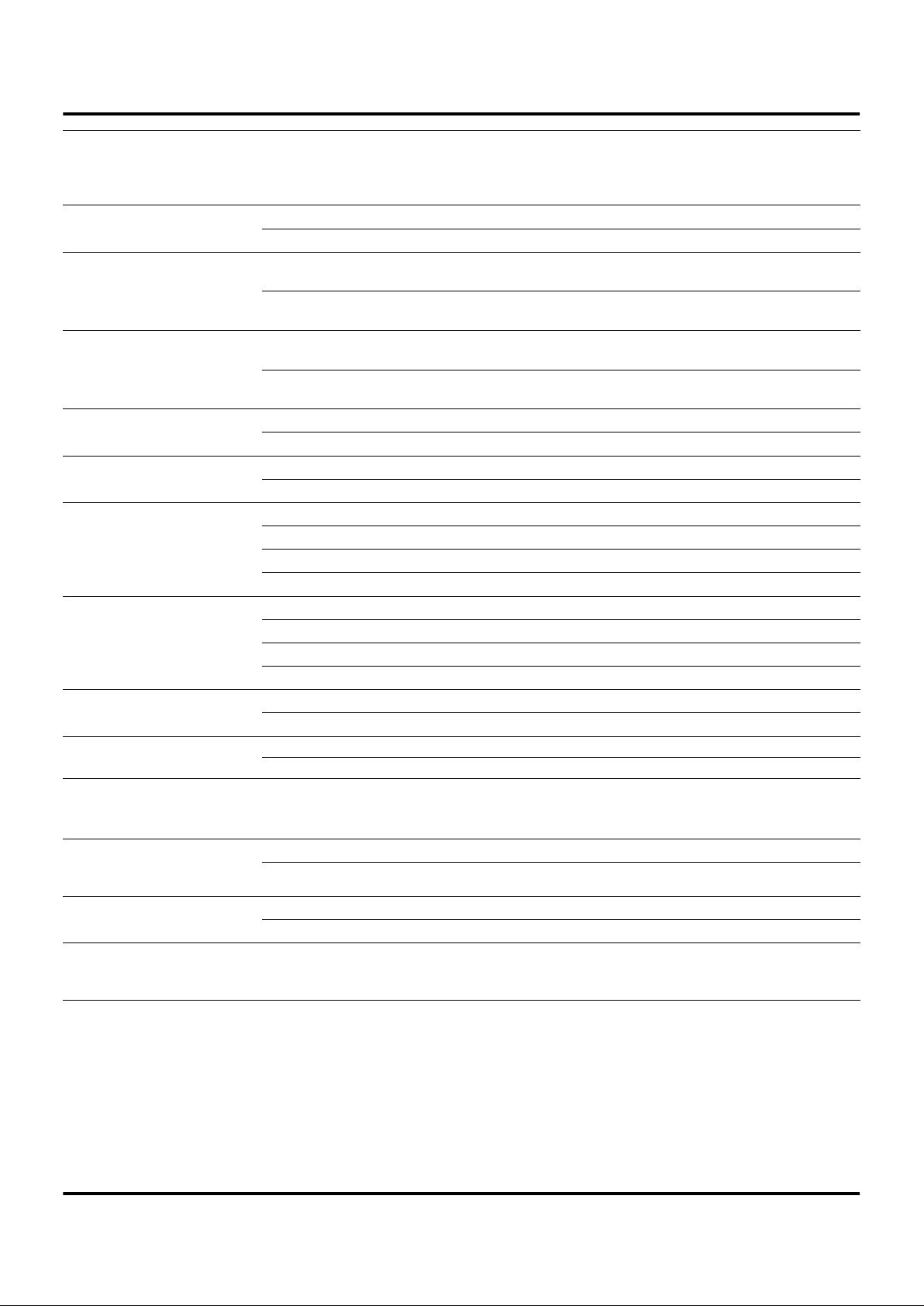
Figure 2. EPROM Programming Mode Block Diagram
Address
MUX
EPROM
ROM PROT
Low Noise
AD 11- 0
Z8 MCU
Z8
Port 0
MSN
Port 3
PGM + Test
Mode Logic
EPM
P32
/CE
XT1
/PGM
P30
D7 - 0
AD 11- 0
AD 11- 0
Data
MUX
Z8
Port 2
D7 - 0
/OE
P31
VPP
P33
D7 - 0
Z86E04/E08
Zilog CMOS Z8 OTP Microcontrollers
DS97Z8X0401
P R E L I M I N A R Y
5
1
PIN DESCRIPTION
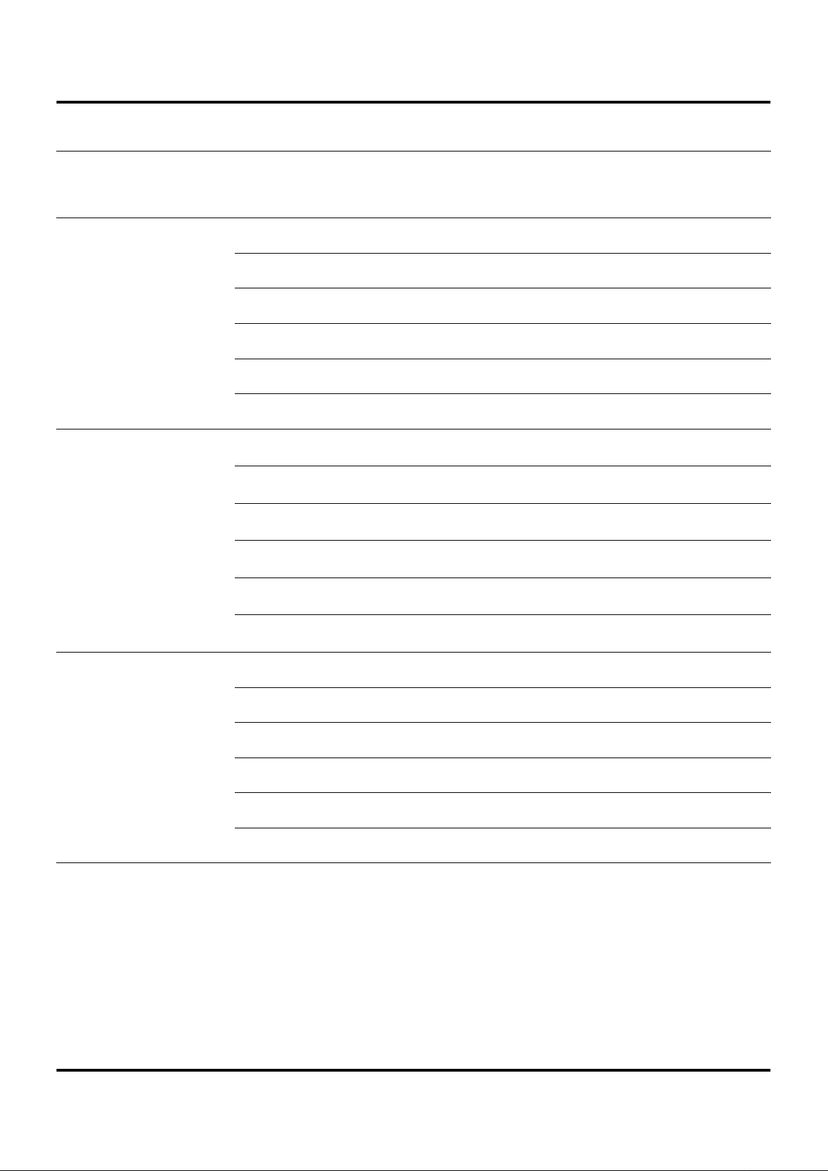
Figure 3. 18-Pin EPROM Mode Configuration
Table 1. 18-Pin DIP Pin Identification
EPROM Programming Mode
Pin # Symbol Function Direction
1–4 D4–D7 Data 4, 5, 6, 7 In/Output
5V
CC
Power Supply
6 N/C No Connection
7 /CE Chip Enable Input
8 /OE Output Enable Input
9 EPM EPROM Prog Mode Input
10 V
PP
Prog V oltage Input
11 Clear Clear Clock Input
12 Clock Address Input
13 /PGM Prog Mode Input
14 GND Ground
15–18 D0–D3 Data 0,1, 2, 3 In/Output
D4
D5
D6
D7
VCC
NC
/CE
/OE
EPM
D3
D2
D1
D0
GND
/PGM
CLOCK
CLEAR
VPP
18
1
910
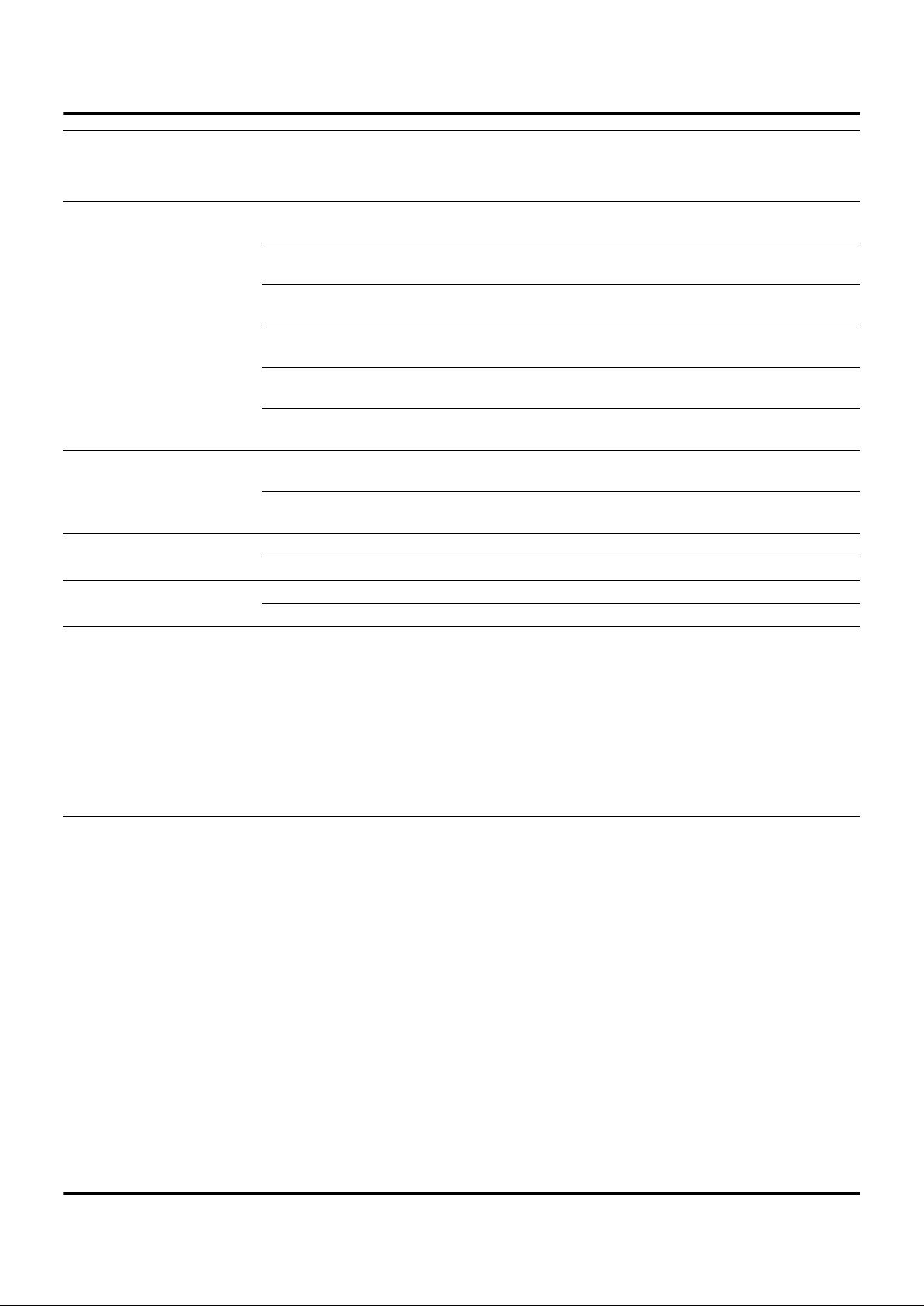
Figure 4. 18-Pin DIP/SOIC Mode Configuration
Table 2. 18-Pin DIP/SOIC Pin Identification
Standard Mode
Pin # Symbol Function Direction
1–4 P24–P27 Port 2, Pins 4,5,6,7 In/Output
5V
cc
Power Supply
6 XTAL2 Crystal Osc. Clock Output
7 XTAL1 Crystal Osc. Clock Input
8 P31 Port 3, Pin 1, AN1 Input
9 P32 Port 3, Pin 2, AN2 Input
10 P33 Port 3, Pin 3, REF Input
11–13 P00–P02 Port 0, Pins 0,1,2 In/Output
14 GND Ground
15–18 P20–P23 Port 2, Pins 0,1,2,3 In/Output
P24
P25
P26
P27
VCC
XTAL2
XTAL1
P31
P32
P23
P22
P21
P20
GND
P02
P01
P00
P33
18
1
910
Z86E04/E08
CMOS Z8 OTP Microcontrollers Zilog
6
P R E L I M I N A R Y
DS97Z8X0401
ABSOLUTE MAXIMUM RATINGS
Stresses greater than those listed under Absolute Maxi-
mum Ratings may cause permanent damage to the de-
vice. This is a stress rating only; functional operation of the
device at any condition above those indicated in the oper-
ational sections of these specifications is not implied. Ex-
posure to absolute maximum rating conditions for an ex-
tended period may affect device reliability. Total power
dissipation should not exceed 462 mW for the package.
Power dissipation is calculated as follows:
Total Power Dissipation = V
DD
x [I
DD
- (sum of I
OH
)]
+ sum of [(V
DD
- V
OH
) x I
OH
]
+ sum of (V
0L
x I
0L
)
Parameter Min Max Units Note
Ambient Temperature under Bias –40 +105 C
Storage Temperature –65 +150 C
Voltage on any Pin with Respect to V
SS
–0.7 +12 V 1
Voltage on V
DD
Pin with Respect to V
SS
–0.3 +7 V
Voltage on Pins 7, 8, 9, 10 with Respect to V
SS
–0.6 V
DD
+1 V 2
Total Power Dissipation 1.65 W
Maximum Allowable Current out of V
SS
300 mA
Maximum Allowable Current into V
DD
220 mA
Maximum Allowable Current into an Input Pin –600 +600 µA3
Maximum Allowable Current into an Open-Drain Pin –600 +600 µA4
Maximum Allowable Output Current Sinked by Any I/O Pin 25 mA
Maximum Allowable Output Current Sourced by Any I/O Pin 25 mA
Total Maximum Output Current Sinked by a Port 60 mA
Total Maximum Output Current Sourced by a Port 45 mA
Notes:
1. This applies to all pins except where otherwise noted. Maximum current into pin must be ± 600 µA.
2. There is no input protection diode from pin to V
DD
(not applicable to EPROM Mode).
3. This excludes Pin 6 and Pin 7.
4. Device pin is not at an output Low state.
Z86E04/E08
Zilog CMOS Z8 OTP Microcontrollers
DS97Z8X0401 P R E L I M I N A R Y 7
1
STANDARD TEST CONDITIONS
The characteristics listed below apply for standard test
conditions as noted. All voltages are referenced to
Ground. Positive current flows into the referenced pin (Fig-
ure 5).
CAPACITANCE
T
A
= 25°C, V
CC
= GND = 0V, f = 1.0 MHz, unmeasured pins returned to GND.
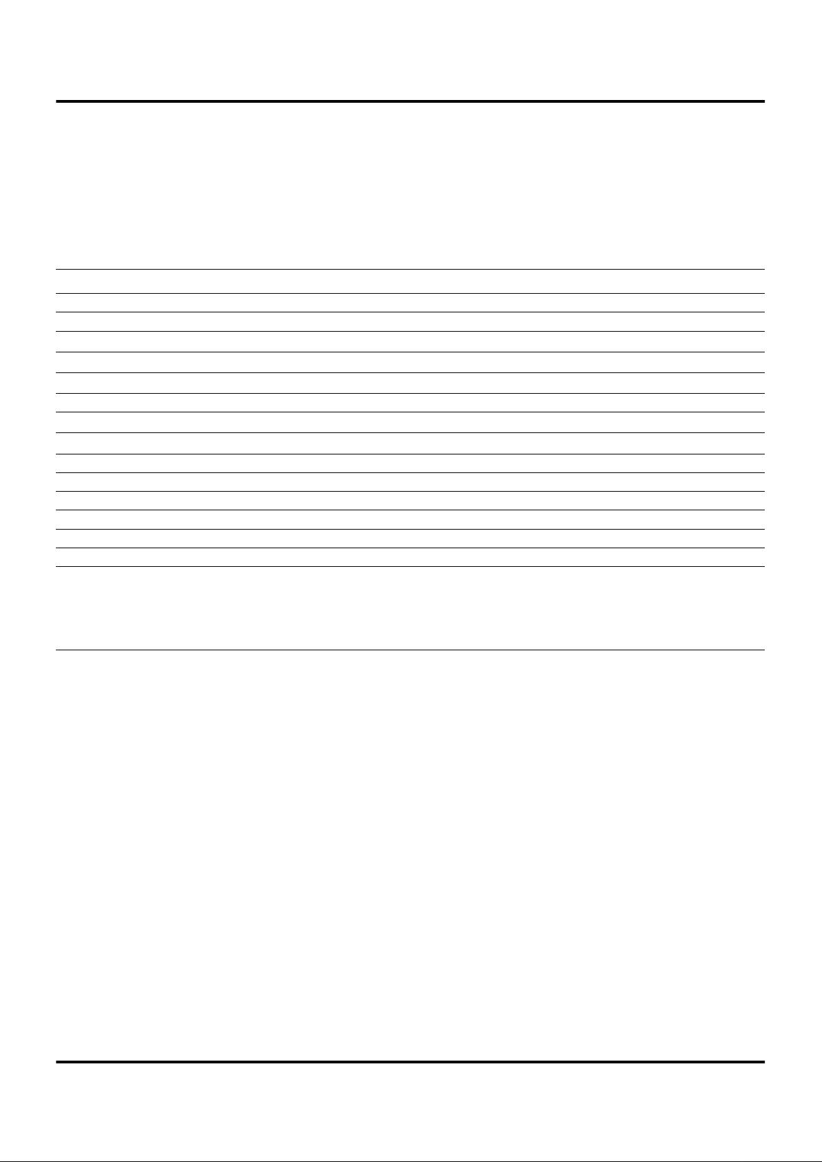
Figure 5. Test Load Diagram
From Output
Under Test
150 pF
Parameter Min Max
Input capacitance 0 10 pF
Output capacitance 0 20 pF
I/O capacitance 0 25 pF
Z86E04/E08
CMOS Z8 OTP Microcontrollers Zilog
8 P R E L I M I N A R Y DS97Z8X0401
DC ELECTRICAL CHARACTERISTICS
T
A
= 0°C to +70°C
Typical
Note 4
Sym Parameter
V
CC
[4]
Min Max @ 25°C Units Conditions Notes
V
INMAX
Max Input Voltage 3.0V 12 V I
In
<250 µA 1
5.5V 12 V I
In
<250 µA 1
V
CH
Clock Input High
Voltage
3.0V 0.8 V
CC
V
CC
+0.3 1.7 V Driven by External
Clock Generator
5.5V 0.8 V
CC
V
CC
+0.3 2.8 V Driven by External
Clock Generator
V
CL
Clock Input Low
Voltage
3.0V V
SS
–0.3 0.2 V
CC
0.8 V Driven by External
Clock Generator
5.5V V
SS
–0.3 0.2 V
CC
1.7 V Driven by External
Clock Generator
V
IH
Input High Voltage 3.0V
5.5V
0.7 V
CC
0.7 V
CC
V
CC
+0.3
V
CC
+0.3
1.8
2.8
V
V
V
IL
Input Low Voltage 3.0V
5.5V
V
SS
–0.3
V
SS
–0.3
0.2 V
CC
0.2 V
CC
0.8
1.5
V
V
V
OH
Output High Voltage 3.0V V
CC
–0.4 3.0 V I
OH
= –2.0 mA 5
5.5V V
CC
–0.4 4.8 V I
OH
= –2.0 mA 5
3.0V V
CC
–0.4 3.0 V Low Noise @ I
OH
= –0.5 mA
5.5V V
CC
–0.4 4.8 V Low Noise @ I
OH
= –0.5 mA
V
OL1
Output Low Voltage 3.0V 0.8 0.2 V I
OL
= +4.0 mA 5
5.5V 0.4 0.1 V I
OL
= +4.0 mA 5
3.0V 0.4 0.2 V Low Noise @ I
OL
= 1.0 mA
5.5V 0.4 0.1 V Low Noise @ I
OL
= 1.0 mA
V
OL2
Output Low Voltage 3.0V 1.0 1.0 V I
OL
= +12 mA, 5
5.5V 0.8 0.8 V I
OL
= +12 mA, 5
V
OFFSET
Comparator Input
Offset V oltage
3.0V 25.0 10.0 mV
5.5V 25.0 10.0 mV
V
LV
V
CC
Low Voltage
Auto Reset
2.2 3.0 2.8 V @ 6 MHz Max.
Int. CLK Freq.
I
IL
Input Leakage
(Input Bias
Current of
Comparator)
3.0V –1.0 1.0 µAV
IN
= 0V, V
CC
5.5V –1.0 1.0 µAV
IN
= 0V, V
CC
I
OL
Output Leakage 3.0V –1.0 1.0 µAV
IN
= 0V, V
CC
5.5V –1.0 1.0 µAV
IN
= 0V, V
CC
V
ICR
Comparator Input
Common Mode
Voltage Range
0V
CC
–1.0 V
Z86E04/E08
Zilog CMOS Z8 OTP Microcontrollers
DS97Z8X0401 P R E L I M I N A R Y 9
1
T
A
= 0°C to +70°C
Typical
Note 4
Sym Parameter
V
CC
[4]
Min Max @ 25°C Units Conditions Notes
I
CC
Supply Current 3.0V 3.5 1.5 mA All Output and I/O Pins
Floating @ 2 MHz
5,7
5.5V 11.0 6.8 mA All Output and I/O Pins
Floating @ 2 MHz
5,7
3.0V 8.0 3.0 mA All Output and I/O Pins
Floating @ 8 MHz
5,7
5.5V 15.0 8.2 mA All Output and I/O Pins
Floating @ 8 MHz
5,7
3.0V 10.0 3.6 mA All Output and I/O Pins
Floating @ 12 MHz
5,7
5.5V 20.0 12.0 mA All Output and I/O Pins
Floating @ 12 MHz
5,7
I
CC1
Standby Current 3.0V 2.5 0.7 mA HALT Mode V
IN
= 0V,V
CC
@ 2 MHz
5,7
5.5V 4.0 2.5 mA HALT Mode V
IN
= 0V,V
CC
@ 2 MHz
5,7
3.0V 4.0 1.0 mA HALT Mode V
IN
= 0V, V
CC
@ 8 MHz
5,7
5.5V 5.0 3.0 mA HALT Mode V
IN
= 0V, V
CC
@ 8 MHz
5,7
3.0V 4.5 1.5 mA HALT Mode V
IN
= 0V, V
CC
@ 12 MHz
5,7
5.5V 7.0 4.0 mA HALT Mode V
IN
= 0V, V
CC
@ 12 MHz
5,7
I
CC
Supply Current
(Low Noise Mode)
3.0V 3.5 1.5 mA All Output and I/O Pins
Floating @ 1 MHz
7
5.5V 11.0 6.8 mA All Output and I/O Pins
Floating @ 1 MHz
7
3.0V 5.8 2.5 mA All Output and I/O Pins
Floating @ 2 MHz
7
5.5V 13.0 7.5 mA All Output and I/O Pins
Floating @ 2 MHz
7
3.0V 8.0 3.0 mA All Output and I/O Pins
Floating @ 4 MHz
7
5.5V 15.0 8.2 mA All Output and I/O Pins
Floating @ 4 MHz
7
Z86E04/E08
CMOS Z8 OTP Microcontrollers Zilog
10 P R E L I M I N A R Y DS97Z8X0401
DC ELECTRICAL CHARACTERISTICS (Continued)
T
A
= 0°C to
+70°C
Typical
Note 4
Sym Parameter
V
CC
[4]
Min Max @ 25°C Units Conditions Notes
I
CC1
Standby Current
(Low Noise Mode)
3.0V 2.5 0.7 mA HALT Mode V
IN
= 0V,V
CC
@ 1 MHz
7
5.5V 4.0 2.5 mA HALT Mode V
IN
= 0V,V
CC
@ 1 MHz
7
3.0V 3.0 0.9 mA HALT Mode V
IN
= 0V,V
CC
@ 2 MHz
7
5.5V 4.5 2.8 mA HALT Mode V
IN
= 0V,V
CC
@ 2 MHz
7
3.0V 4.0 1.0 mA HALT Mode V
IN
= 0V,V
CC
@ 4 MHz
7
5.5V 5.0 3.0 mA HALT Mode V
IN
= 0V,V
CC
@ 4 MHz
7
I
CC2
Standby Current 3.0V 10.0 1.0 µA STOP Mode V
IN
= 0V, V
CC
WDT is not Running
7,8
5.5V 10.0 1.0 µA STOP Mode V
IN
= 0V,V
CC
WDT is not Running
7,8
I
ALL
Auto Latch Low
Current
3.0V 12.0 3.0 µA 0V < V
IN
< V
CC
5.5V 32 16 µAµ 0V < V
IN
< V
CC
I
ALH
Auto Latch High
Current
3.0V –8.0 –1.5 µAµ 0V < V
IN
< V
CC
5.5V –16.0 –8.0 µA 0V < V
IN
< V
CC
Notes:
1. Port 2 and Port 0 only
2. V
SS
= 0V = GND
3. The device operates down to V
LV
of the specified frequency for V
LV
.
The minimum operational V
CC
is determined on the value of
the voltage V
LV
at the ambient temperature. The V
LV
increases as the temperature decreases.
4. The V
CC
voltage specification of 3.0 V guarantees 3.3 V ± 0.3 V with typical values measured at V
CC
= 3.3V.
The V
CC
voltage specification of 5.5 V guarantees 5.0 V ± 0.5 V with typical values measured at V
CC
= 5.0 V.
5. Standard Mode (not Low EMI Mode)
6. Z86E08 only
7. All outputs unloaded and all inputs are at V
CC
or V
SS
level.
8. If analog comparator is selected, then the comparator inputs must be at V
CC
level.
Z86E04/E08
Zilog CMOS Z8 OTP Microcontrollers
DS97Z8X0401 P R E L I M I N A R Y 11
1
T
A
= -40°C to
+105°C
Typical
Note 4
Sym Parameter
V
CC
[4]
Min Max @ 25°C Units Conditions Notes
V
INMAX
Max Input Voltage 4.5V 12.0 V I
IN
< 250 µA1
5.5V 12.0 V I
IN
< 250 µA1
V
CH
Clock Input High
Voltage
4.5V 0.8 V
CC
V
CC
+0.3 2.8 V Driven by External Clock
Generator
5.5V 0.8 V
CC
V
CC
+0.3 2.8 V Driven by External Clock
Generator
V
CL
Clock Input Low
Voltage
4.5V V
SS
–0.3 0.2 V
CC
1.7 V Driven by External Clock
Generator
5.5V V
SS
–0.3 0.2 V
CC
1.7 V Driven by External Clock
Generator
V
IH
Input High Voltage 4.5V 0.7 V
CC
V
CC
+0.3 2.8 V
5.5V 0.7 V
CC
V
CC
+0.3 2.8 V
V
IL
Input Low Voltage 4.5V V
SS
–0.3 0.2 V
CC
1.5 V
5.5V V
SS
–0.3 0.2 V
CC
1.5 V
V
OH
Output High Voltage 4.5V V
CC
–0.4 4.8 V I
OH
= –2.0 mA 5
5.5V V
CC
–0.4 4.8 V I
OH
= –2.0 mA 5
4.5V V
CC
–0.4 V Low Noise @ I
OH
= –0.5 mA
5.5V V
CC
–0.4 V Low Noise @ I
OH
= –0.5 mA
V
OL1
Output Low Voltage 4.5V 0.4 0.1 V I
OL
= +4.0 mA 5
5.5V 0.4 0.1 V I
OL
= +4.0 mA 5
4.5V 0.4 0.1 V Low Noise @ I
OL
= 1.0 mA
5.5V 0.4 0.1 V Low Noise @ I
OL
= 1.0 mA
V
OL2
Output Low Voltage 4.5V 1.0 0.3 V I
OL
= +12 mA, 5
5.5V 1.0 0.3 V I
OL
= +12 mA, 5
V
OFFSET
Comparator Input
Offset V oltage
4.5V 25.0 10.0 mV
5.5V 25.0 10.0 mV
V
LV
V
CC
Low Voltage
Auto Reset
1.8 3.8 2.8 V @ 6 MHz Max. Int.
CLK Freq.
3
I
IL
Input Leakage
(Input Bias Current
of Comparator)
4.5V –1.0 1.0 µAV
IN
= 0V, V
CC
5.5V –1.0 1.0 µAV
IN
= 0V, V
CC
I
OL
Output Leakage 4.5V –1.0 1.0 µAV
IN
= 0V, V
CC
5.5V –1.0 1.0 µAV
IN
= 0V, V
CC
V
ICR
Comparator Input
Common Mode
Voltage Range
0 V
CC
–1.5 V
Z86E04/E08
CMOS Z8 OTP Microcontrollers Zilog
12 P R E L I M I N A R Y DS97Z8X0401
DC ELECTRICAL CHARACTERISTICS (Continued)
I
CC
Supply Current 4.5V 11.0 6.8 mA All Output and I/O Pins
Floating @ 2 MHz
5,7
5.5V 11.0 6.8 mA All Output and I/O Pins
Floating @ 2 MHz
5,7
4.5V 15.0 8.2 mA All Output and I/O Pins
Floating @ 8 MHz
5,7
5.5V 15.0 8.2 mA All Output and I/O Pins
Floating @ 8 MHz
5,7
4.5V 20.0 12.0 mA All Output and I/O Pins
Floating @ 12 MHz
5,7
5.5V 20.0 12.0 mA All Output and I/O Pins
Floating @ 12 MHz
5,7
I
CC1
Standby Current 4.5V 5.0 2.5 mA HALT Mode V
IN
= 0V, V
CC
@ 2 MHz
5,7
5.5V 5.0 2.5 mA HALT Mode V
IN
= 0V, V
CC
@ 2 MHz
5,7
4.5V 5.0 3.0 mA HALT Mode V
IN
= 0V, V
CC
@ 8 MHz
5,7
5.5V 5.0 3.0 mA HALT Mode V
IN
= 0V, V
CC
@ 8 MHz
5,7
4.5V 7.0 4.0 mA HALT Mode V
IN
= 0V, V
CC
@ 12 MHz
5,7
5.5V 7.0 4.0 mA HALT Mode V
IN
= 0V, V
CC
@ 12 MHz
5,7
I
CC
Supply Current
(Low Noise Mode)
4.5V 11.0 6.8 mA All Output and I/O Pins
Floating @ 1 MHz
7
5.5V 11.0 6.8 mA All Output and I/O Pins
Floating @ 1 MHz
7
4.5V 13.0 7.5 mA All Output and I/O Pins
Floating @ 2 MHz
7
5.5V 13.0 7.5 mA All Output and I/O Pins
Floating @ 2 MHz
7
4.5V 15.0 8.2 mA All Output and I/O Pins
Floating @ 4 MHz
7
5.5V 15.0 8.2 mA All Output and I/O Pins
Floating @ 4 MHz
7
T
A
= -40°C to
+105°C
Typical
Note 4
Sym Parameter
V
CC
[4]
Min Max @ 25°C Units Conditions Notes
Z86E04/E08
Zilog CMOS Z8 OTP Microcontrollers
DS97Z8X0401 P R E L I M I N A R Y 13
1
T
A
= -40°C to
+105°C
Typical
Note 4
Sym Parameter
V
CC
[4]
Min Max @ 25°C Units Conditions Notes
I
CC1
Standby Current
(Low Noise Mode)
4.5V 4.0 2.5 mA HALT Mode V
IN
= 0V, V
CC
@ 1 MHz
7
5.5V 4.0 2.5 mA HALT Mode V
IN
= 0V, V
CC
@ 1 MHz
7
4.5V 4.5 2.8 mA HALT Mode V
IN
= 0V, V
CC
@ 2 MHz
7
5.5V 4.5 2.8 mA HALT Mode V
IN
= 0V, V
CC
@ 2 MHz
7
4.5V 5.0 3.0 mA HALT Mode V
IN
= 0V, V
CC
@ 4 MHz
7
5.5V 5.0 3.0 mA HALT Mode V
IN
= 0V, V
CC
@ 4 MHz
7
I
CC2
Standby Current 4.5V 20 1.0 µA STOP Mode V
IN
= 0V, V
CC
WDT is not Running
7,8
5.5V 20 1.0 µA STOP Mode V
IN
= 0V, V
CC
WDT is not Running
7,8
I
ALL
Auto Latch Low
Current
4.5V 40 16 µA 0V < V
IN
< V
CC
5.5V 40 16 µA 0V < V
IN
< V
CC
I
ALH
Auto Latch High
Current
4.5V –20.0 –8.0 µA 0V < V
IN
< V
CC
5.5V –20.0 –8.0 µA 0V < V
IN
< V
CC
Notes:
1. Port 2 and Port 0 only
2. V
SS
= 0V = GND
3. The device operates down to V
LV
of the specified frequency for V
LV
.
The minimum operational V
CC
is determined on the value of
the voltage V
LV
at the ambient temperature. The V
LV
increases as the temperature decreases.
4. V
CC
= 4.5V to 5.5V, typical values measured at V
CC
= 5.0V
5. Standard Mode (not Low EMI Mode)
6. Z86E08 only
7. All outputs unloaded and all inputs are at V
CC
or V
SS
level.
8. If analog comparator is selected, then the comparator inputs must be at V
CC
level.
Z86E04/E08
CMOS Z8 OTP Microcontrollers Zilog
14 P R E L I M I N A R Y DS97Z8X0401
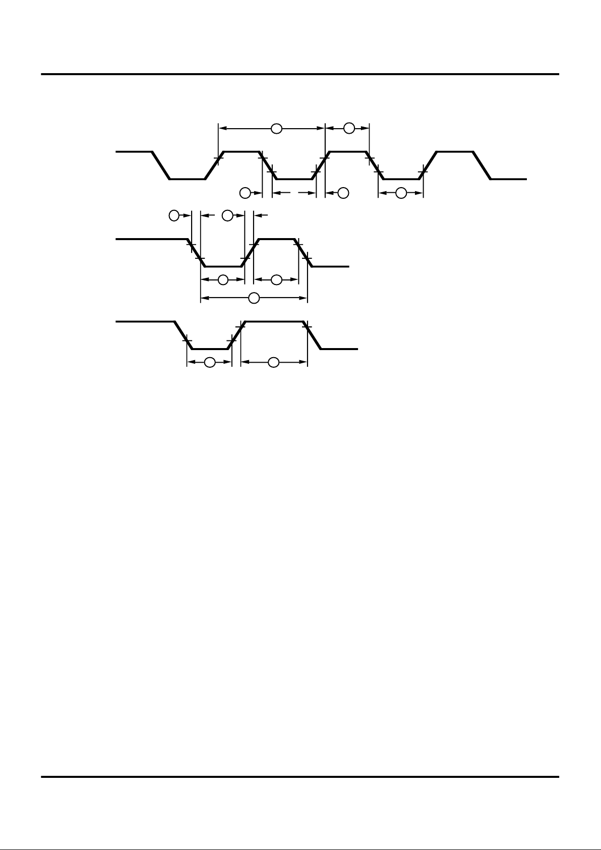
AC ELECTRICAL CHARACTERISTICS
Figure 6. AC Electrical Timing Diagram
1
3
4
8
2
2
3
T
IRQ
IN
N
6
5
7
7
9
Clock
 Loading...