


ZILOG Z86C6320VEC, Z86C6320VSC, Z86C6416PEC, Z86C6416PSC, Z86C6416VEC Datasheet
...
|
P R E L I M I N A R Y |
Z86C63/64 |
|
|
CPS DC-5461-02 |
|
|
|
|
|
|
PRELIMINARY
CUSTOMER PROCUREMENT SPECIFICATION
Z86C63/64
CMOS Z8®
32K ROM MICROCONTROLLER
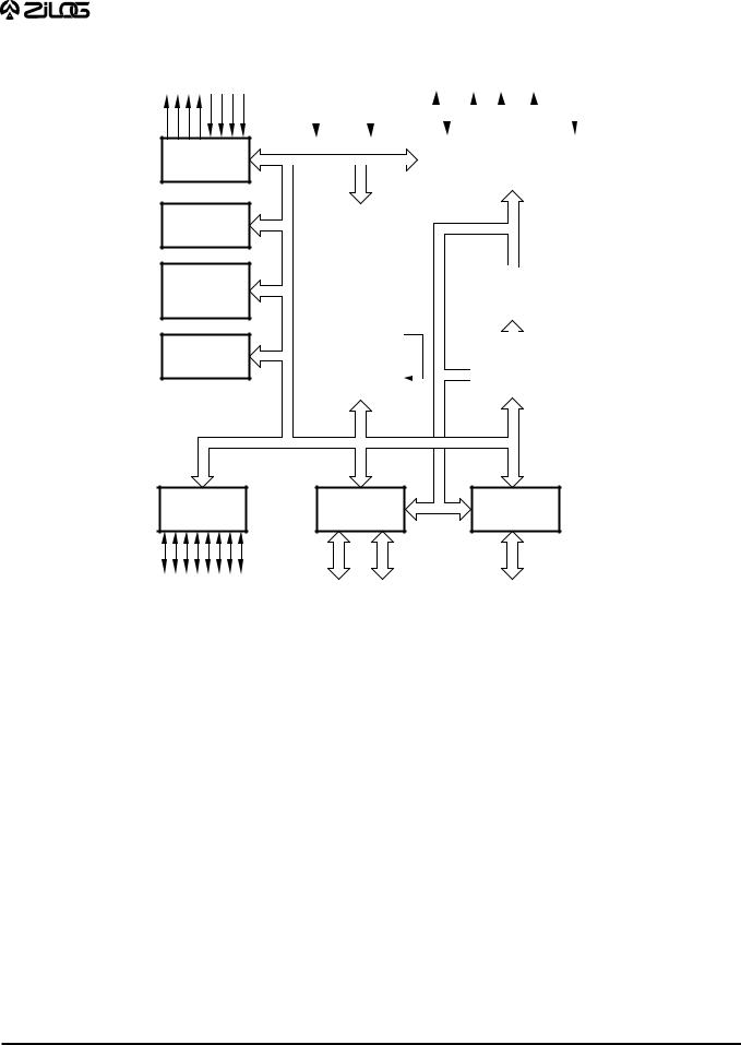
GENERAL DESCRIPTION
The Z86C63/64 microcontroller introduces a new level of sophistication to single-chip architecture. The Z86C63/64 is a member of the Z8 single-chip microcontroller family with 32 Kbytes of ROM and 256 bytes of RAM.
The Z86C63 is housed in a 40-pin DIP, and a 44-pin PLCC package, and is manufactured in CMOS technology. The ROMless pin option is available on the 44-pin version only. The Z86C64 is housed in a 64-pin DIP, and a 68-pin PLCC. Both versions of the Z86C64 have the ROMless pin option, which allows both external memory and preprogrammed ROM, enabling this Z8 microcontroller to be used in highvolume applications or where code flexibility is required. The Z86C96 ROMless Z8 will support the Z86C63/64.
Zilog’s CMOS microcontroller offers fast execution, more efficient use of memory, more sophisticated interrupts, input/output bit manipulation capabilities, and easy hardware/software system expansion along with low cost and low power consumption.
The Z86C63/64 architecture is characterized by Zilog’s 8-bit microcontroller core. The device offers a flexible I/O scheme, an efficient register and address space structure, multiplexed capabilities between address/data, I/O, and a number of ancillary features that are useful in many industrial and advanced scientific applications.
For applications which demand powerful I/O capabilities, the Z86C63 fulfills this with 32 pins dedicated to input and output. These lines are grouped into four ports with eight lines each. The Z86C64 has 52 pins for input and output, and these lines are grouped into six, 8-bit ports and one 4-bit port. Each port is configurable under software control to provide timing, status signals, serial or parallel I/O with or without handshake, and an address/data bus for interfacing external memory.
There are three basic address spaces available to support this wide range of configurations: Program Memory, Data Memory, and 236 General-Purpose Registers.
To unburden the program from coping with the real-time problems such as counting/timing and serial data communication, the Z86C63/64 offers two on-chip counter/timers with a large number of user selectable modes, and an asynchronous receiver/transmitter (UART) (see Block Diagrams).
Notes:
All Signals with a preceding front slash, "/", are active Low, e.g., B//W (WORD is active Low); /B/W (BYTE is active Low, only).
Power connections follow conventional descriptions below:
Connection |
Circuit |
Device |
|
|
|
Power |
VCC |
VDD |
Ground |
GND |
VSS |
DC-5461-02 (12-13-93) |
1 |
P R E L I M I N A R Y |
Z86C63/64 |
CPS DC-5461-02 |
GENERAL DESCRIPTION
Output Input
Port 3
UART
Counter/
Timers
(2)
Interrupt
Control
Port 2
I/O
(Bit Programmable)
Vcc |
|
GND |
|
XTAL /AS /DS R//W /RESET |
||||||||||||||||
|
|
|
|
|
|
|
|
|
|
|
|
|
|
|
|
|
|
|
|
|
|
|
|
|
|
|
|
|
|
|
|
|
|
|
|
|
|
|
|
|
|
|
|
|
|
|
|
|
|
|
|
|
|
|
|
|
|
|
|
|
|
|
|
|
|
|
|
|
|
|
|
|
|
Machine Timing and |
|
||||||||
|
|
|
|
|
|
|
|
|
|
|
Instruction Control |
|
||||||||
|
|
|
|
|
|
|
|
|
|
|
|
|||||||||
|
|
|
|
|
|
|
|
|
|
|
|
|
|
|
|
|
|
|
|
|
|
|
|
|
|
|
|
|
|
|
|
|
|
|
|
|
|
|
|
|
|
|
|
ALU |
|
|
|
|
|
|
|
|
|
|
|
|
|
|
|
|||
|
|
|
|
|
|
|
|
|
|
|
|
|
|
|
|
|
|
|
|
|
|
|
FLAGS |
|
|
|
|
|
|
|
|
|
|
|
|
|
|
|
|||
|
|
|
|
|
|
|
|
|
Prg. Memory |
|
|
|
||||||||
|
|
|
|
|
|
|
|
|
|
|
|
|
|
|
||||||
|
|
|
|
|
|
|
|
|
|
32,768 |
|
|
|
|
||||||
|
|
|
|
|
|
|
|
|
||||||||||||
|
|
|
|
|
|
|
|
|
|
|
|
|
x 8-Bit |
|
|
|||||
|
|
Register |
|
|
|
|
|
|
|
|
|
|
|
|
|
|
|
|||
|
|
Pointer |
|
|
|
|
|
|
|
|
|
|
|
|
|
|
|
|||
|
|
|
|
|
|
|
|
|
|
|
|
|
|
|
|
|
|
|
||
|
Register File |
|
|
|
|
|
|
|
Program |
|
|
|||||||||
|
|
256 x 8-Bit |
|
|
|
|
|
|
|
Counter |
|
|
||||||||
|
|
|
|
|
|
|
|
|
|
|
|
|||||||||
|
|
|
|
|
|
|
|
|
|
|
|
|
|
|
|
|
|
|
|
|
Port 0 |
Port 1 |
|
4 |
4 |
8 |
Address or I/O |
Address/Data or I/O |
|
(Nibble Programmable) |
(Byte Programmable) |
|
Z86C63 Functional Block Diagram
2

P R E L I M I N A R Y |
|
Z86C63/64 |
|
|
CPS DC-5461-02 |
||
Output Input |
Vcc |
GND |
XTAL /AS /DS R//W /RESET |
|
|
|
|
|
|
|
|
|
|
|
|
|
|
|
|
|
|
|
|
|
|
|
|
|
|
|
|
|
|
|
|
|
|
|
|
|
|
|
|
|
|
|
|
|
|
|
|
|
|
|
|
|
|
|
|
|
|
|
|
|
|
|
|
|
|
|
|
|
|
|
|
|
|
|
|
|
|
|
|
|
|
|
|
Port 3 |
|
|
|
|
|
|
|
|
|
|
Machine Timing and |
||||||||||||
|
|
|
|
|
|
|
|
|
|
|
|
|
|
|
|
|
|
|
|
Instruction Control |
||||||
|
|
|
|
|
|
|
|
|
|
|
|
|
|
|
|
|
|
|
|
|
|
|
|
|
|
|
|
|
|
|
|
|
|
|
|
|
|
|
|
|
|
|
|
|
|
|
|
|
|
|
|
|
|
|
|
|
UART |
|
|
|
ALU |
|
|
|
|
|
|
|
|
|
|
|
|
|
||||||
|
|
|
|
|
|
|
|
|
|
|
|
|
|
|
||||||||||||
|
|
|
|
|
|
|
|
|
|
|
|
|
|
|
|
|
|
|
|
|
|
|
|
|
|
|
|
|
|
|
|
|
|
|
|
|
|
|
|
|
|
|
|
|
|
|
|
|
|
|
|
|
|
|
|
|
|
|
|
|
|
|
|
|
|
Flags |
|
|
|
|
|
|
|
Program |
|
|||||
|
|
Counter/ |
|
|
|
|
|
|
|
|
|
|
|
|
Memory |
|
||||||||||
|
|
Timers (2) |
|
|
|
|
|
|
|
|
|
|
|
32,768 x 8-Bit |
|
|||||||||||
|
|
|
|
|
|
|
|
|
|
|
|
|
|
|
|
|
|
|
|
|||||||
|
|
|
|
|
|
|
|
|
|
|
|
|
|
|
|
|
|
|
|
|
|
|
|
|
|
|
|
|
|
|
|
|
|
|
|
|
|
|
Register |
|
|
|
|
|
|
|
|
|
|
|
|
|
|
|
|
|
|
|
|
|
|
|
|
|
|
|
|
|
|
|
|
|
|
|
|
|
|
|
||
|
|
|
|
|
|
|
|
|
|
|
|
Pointer |
|
|
|
|
|
|
|
Program |
|
|
||||
|
|
Interrupt |
|
|
|
|
|
|
|
|
|
|
|
|
Counter |
|
|
|||||||||
|
|
|
|
|
|
|
|
|||||||||||||||||||
|
|
Control |
|
|
Register File |
|
|
|
|
|
|
|
|
|
|
|
|
|
||||||||
|
|
|
|
|
|
|
|
|
|
|
|
|
|
|
||||||||||||
|
|
|
|
|
|
|
|
|
|
|
|
|
|
|
|
|
|
|
|
|
|
|
|
|||
|
|
|
|
|
|
|
|
|
|
|
|
256 x 8-Bit |
|
|
|
|
|
|
|
|
|
|
|
|
|
|
|
|
|
|
|
|
|
|
|
|
|
|
|
|
|
|
|
|
|
|
|
||||||
|
|
|
|
|
|
|
|
|
|
|
|
|
|
|
|
|
|
|
|
|
|
|
|
|
|
|
|
|
|
|
|
|
|
|
|
|
|
|
|
|
|
|
|
|
|
|
|
|
|
|
|
|
|
|
|
Port 6 |
|
|
|
|
Port 5 |
|
|
|
|
Port 4 |
|
|
|
|
Port 2 |
|
|
|
Port 0 |
|
|
Port 1 |
|
||||||||||||||||||
|
|
|
|
|
|
|
|
|
|
|
|
|
|
|
|
|
|
|
|
|
|
|
|
|
|
|
|
|
|
|
|
|
|
|
|
|
|
|
|
|
|
|
|
|
|
|
|
|
|
|
|
|
|
|
|
|
|
|
|
|
|
|
|
|
|
|
|
|
|
|
|
|
|
|
|
|
|
|
|
|
4 |
4 |
|
8 |
|
||
|
|
|
|
|
|
|
|
|
|
|
|
|
|
|
|
|
|
|
|
|
|
|
|
|
|
|
|
|
|
|
|
|
|
|
|
|
|
|
|||||
|
|
|
|
|
|
|
|
|
|
|
|
|
|
|
|
|
|
|
|
|
|
|
|
|
|
|
|
|
|
I/O |
|
Address or I/O |
Address/Data or I/O |
||||||||||
|
|
|
|
|
|
|
|
|
|
|
|
|
|
|
|
|
|
|
|
|
|
|
|
|
|
|
|
|
|
|
|||||||||||||
|
|
|
|
|
|
|
|
|
|
|
I/O |
|
|
|
|
|
|
|
|
|
(Bit Programmable) |
(Nibble Programmable) |
(Byte Programmable) |
||||||||||||||||||||
|
|
|
|
|
|
|
|
|
|
|
|
|
|
|
|
|
|
|
|
|
|
|
|
|
|
|
|
|
|
|
|
|
|
|
|
|
|
||||||
(Bit Programmable)
Z86C64 Functional Block Diagram
3

P R E L I M I N A R Y |
Z86C63/64 |
CPS DC-5461-02 |
PIN DESCRIPTION
VCC |
|
1 |
|
40 |
|
P36 |
|
|
|
||||
XTAL2 |
|
2 |
|
39 |
|
P31 |
|
|
|
||||
XTAL1 |
|
3 |
|
38 |
|
P27 |
|
|
|
||||
P37 |
|
4 |
|
37 |
|
P26 |
|
|
|
||||
P30 |
|
5 |
|
36 |
|
P25 |
|
|
|
||||
/RESET |
|
6 |
|
35 |
|
P24 |
|
|
|
||||
R//W |
|
7 |
|
34 |
|
P23 |
|
|
|
||||
/DS |
|
8 |
|
33 |
|
P22 |
|
|
|
||||
/AS |
|
9 |
|
32 |
|
P21 |
|
|
|
||||
P35 |
|
10 |
Z86C63 |
31 |
|
P20 |
|
|
|||||
|
|
|
30 |
|
|
|
GND |
|
11 |
DIP |
|
P33 |
|
P32 |
|
12 |
|
29 |
|
P34 |
|
|
|
||||
P00 |
|
13 |
|
28 |
|
P17 |
|
|
|
||||
P01 |
|
14 |
|
27 |
|
P16 |
|
|
|
||||
P02 |
|
15 |
|
26 |
|
P15 |
|
|
|
||||
P03 |
|
16 |
|
25 |
|
P14 |
|
|
|
||||
P04 |
|
17 |
|
24 |
|
P13 |
|
|
|
||||
P05 |
|
18 |
|
23 |
|
P12 |
|
|
|
||||
P06 |
|
19 |
|
22 |
|
P11 |
|
|
|
||||
P07 |
|
20 |
|
21 |
|
P10 |
|
|
|
||||
|
|
|
|
|
|
|
Z86C63 40-Pin DIP
Pin Assignments
Z86C63 40-Pin DIP Pin Identification
Pin # |
Symbol |
Function |
Direction |
|
|
|
|
1 |
VCC |
Power Supply |
Input |
2 |
XTAL2 |
Crystal, Oscillator Clock |
Output |
3 |
XTAL1 |
Crystal, Oscillator Clock |
Input |
4 |
P37 |
Port 3, Pin 7 |
Output |
5 |
P30 |
Port 3, Pin 0 |
Input |
|
|
|
|
6 |
/RESET |
Reset |
Input |
7 |
R//W |
Read/Write |
Output |
8 |
/DS |
Data Strobe |
Output |
9 |
/AS |
Address Strobe |
Output |
10 |
P35 |
Port 3, Pin 5 |
Output |
|
|
|
|
11 |
GND |
Ground |
Input |
12 |
P32 |
Port 3, Pin 2 |
Input |
13-20 |
P07-P00 |
Port 0, Pins 0,1,2,3,4,5,6,7 In/Output |
|
21-28 |
P17-P10 |
Port 1, Pins 0,1,2,3,4,5,6,7 In/Output |
|
29 |
P34 |
Port 3, Pin 4 |
Output |
|
|
|
|
30 |
P33 |
Port 3, Pin 3 |
Input |
31-38 |
P27-P20 |
Port 2, Pins 0,1,2,3,4,5,6,7 In/Output |
|
39 |
P31 |
Port 3, Pin 1 |
Input |
40 |
P36 |
Port 3, Pin 6 |
Output |
|
|
|
|
4
P R E L I M I N A R Y |
Z86C63/64 |
CPS DC-5461-02 |
N/C |
|
P30 |
|
P37 |
|
|
|
|
|
|
|
|
|
|
6 5 4
/RESET 7
R//W 8
/DS 9
/AS 
 10
10
P35 11
GND 
 12
12
P32 13
P00 14
P01 15
P02 16
/ROMless 17
18 |
19 |
20 |
P03 |
P04 |
P05 |
XTAL1
3
21 P06
XTAL2 |
VCC |
P36 |
2 |
1 |
44 |
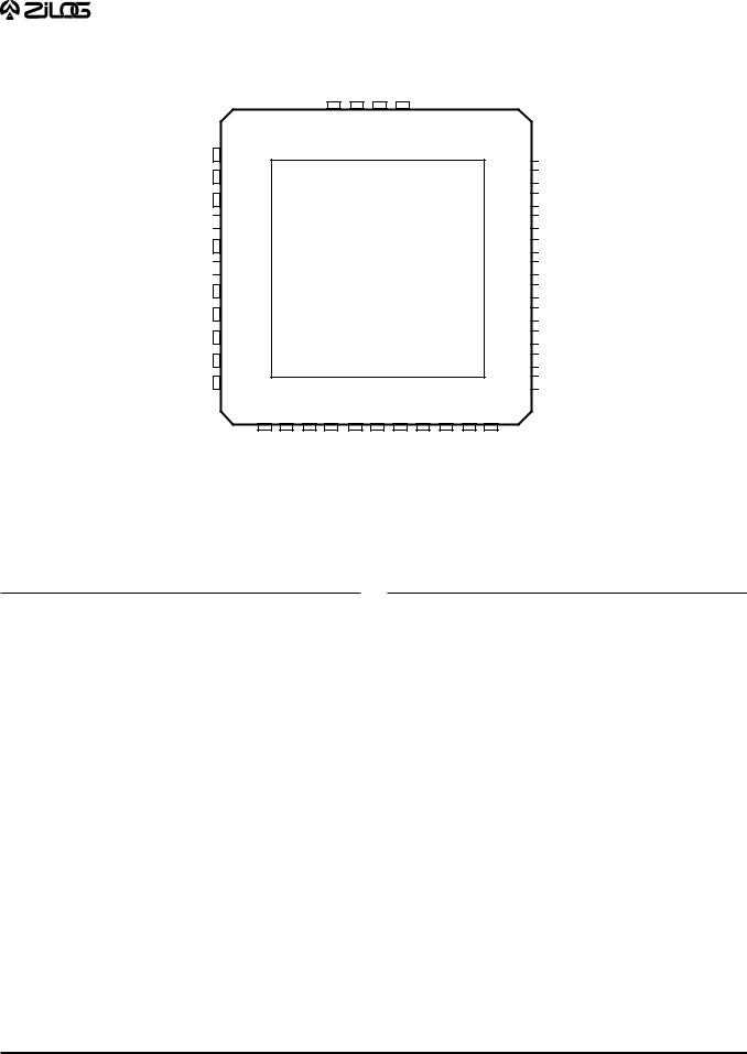
Z86C63 PLCC
22 |
23 |
24 |
P07 |
P10 |
P11 |
P31 |
|
P27 |
|
P26 |
|
P25 |
|
|
|
|
|
|
|
|
|
|
|
|
|
|
43 42 41 40
39 
 N/C
N/C
38 
 P24
P24
37 
 P23
P23
36 
 P22
P22
35 
 P21
P21
34 
 P20
P20
33 
 P33
P33
32 
 P34
P34
31 
 P17
P17
30 
 P16
P16
29 
 P15
P15
25 |
26 |
27 |
28 |
P12 |
P13 |
P14 |
N/C |
|
Z86C63 44-Pin PLCC Pin Assignments |
|
||
|
Z86C63 44-Pin PLCC Pin Identification |
|
||
|
|
|
|
|
Pin # Symbol Function |
Direction |
|
Pin # Symbol Function |
Direction |
1 |
VCC |
Power Supply |
Input |
2 |
XTAL2 |
Crystal, Oscillator Clock |
Output |
3 |
XTAL1 |
Crystal, Oscillator Clock |
Input |
4 |
P37 |
Port 3, Pin 7 |
Output |
5 |
P30 |
Port 3, Pin 0 |
Input |
|
|
|
|
6 |
N/C |
Not Connected |
Input |
7 |
/RESET |
Reset |
Input |
8 |
R//W |
Read/Write |
Output |
9 |
/DS |
Data Strobe |
Output |
10 |
/AS |
Address Strobe |
Output |
|
|
|
|
11 |
P35 |
Port 3, Pin 5 |
Output |
12 |
GND |
Ground |
Input |
13 |
P32 |
Port 3, Pin 2 |
Input |
14-16 |
P02-P00 |
Port 0, Pins 0,1,2 |
In/Output |
|
|
|
|
17 |
/ROMless |
ROM/ROMless control |
Input |
18-22 P07-P03 |
Port 0, Pins 3,4,5,6,7 |
In/Output |
|
23-27 P14-P10 |
Port 1, Pins 0,1,2,3,4 |
In/Output |
|
28 |
N/C |
Not Connected |
Input |
|
|
|
|
29-31 P17-P15 |
Port 1, Pins 5,6,7 |
In/Output |
|
32 |
P34 |
Port 3, Pin 4 |
Output |
33 |
P33 |
Port 3, Pin 3 |
Input |
34-38 P24-P20 |
Port 2, Pins 0,1,2,3,4 |
In/Output |
|
|
|
|
|
39 |
N/C |
Not Connected |
Input |
40-42 P25-P27 |
Port 2, Pins 5,6,7 |
In/Output |
|
43 |
P31 |
Port 3, Pin 1 |
Input |
44 |
P36 |
Port 3, Pin 6 |
Output |
|
|
|
|
5
P R E L I M I N A R Y |
Z86C63/64 |
CPS DC-5461-02 |
PIN DESCRIPTION (Continued)
P44 |
|
1 |
VCC |
|
2 |
|
||
P45 |
|
3 |
|
||
XTAL2 |
|
4 |
|
||
XTAL1 |
|
5 |
|
||
P37 |
|
6 |
|
||
P30 |
|
7 |
|
||
N/C |
|
8 |
|
||
/RESET |
|
9 |
|
||
R//W |
|
10 |
|
||
/DS |
|
11 |
|
||
P46 |
|
12 |
|
||
P47 |
|
13 |
|
||
/AS |
|
14 |
|
||
P35 |
|
15 |
|
||
/ROMless |
|
16 |
|
||
GND |
|
17 |
|
||
P32 |
|
18 |
|
||
P50 |
|
19 |
|
||
P51 |
|
20 |
|
||
P00 |
|
|
|
21 |
|
|
||
P01 |
|
|
|
22 |
|
|
||
P02 |
|
|
|
23 |
|
|
||
P03 |
|
|
|
24 |
|
|
||
P04 |
|
25 |
|
||
P05 |
|
26 |
|
||
P06 |
|
27 |
|
||
P07 |
|
28 |
|
||
VCC |
|
29 |
|
||
P52 |
|
30 |
|
||
P53 |
|
31 |
|
||
P54 |
|
32 |
|
||
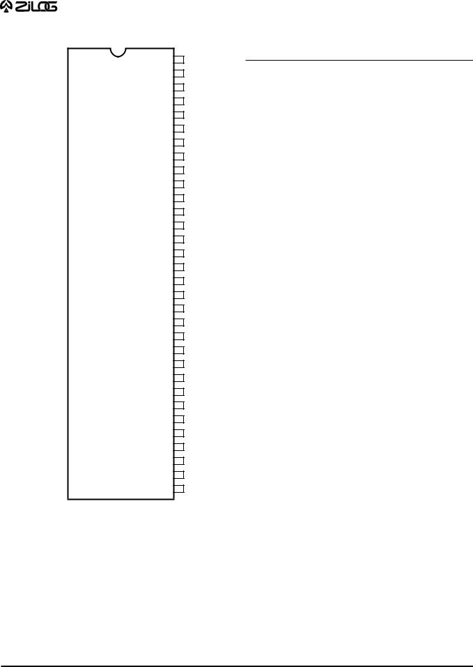
Z86C64
DIP
64 |
P43 |
63 |
P42 |
62 |
P36 |
61 |
P31 |
60 |
P41 |
59 |
P40 |
58 |
P27 |
57 |
P26 |
56 |
P25 |
55 |
P24 |
54 |
P23 |
53 |
P22 |
52 |
P60 |
51 |
P61 |
50 |
P21 |
49 |
P20 |
48 |
GND |
47 |
P33 |
46 |
P34 |
45 |
P62 |
44 |
P63 |
43 |
P17 |
42 |
P16 |
41 |
P15 |
40 |
P14 |
39 |
P13 |
38 |
P12 |
37 |
P57 |
36 |
P56 |
35 |
P11 |
34 |
P10 |
33 |
P55 |
Z86C64 64-Pin DIP Pin Assignments
Z86C64 64-Pin DIP Pin Identification
Pin # |
Symbol |
Function |
Direction |
|
|
|
|
1 |
P44 |
Port 4, Pin 4 |
In/Output |
2 |
VCC |
Power Supply |
Input |
3 |
P45 |
Port 4, Pin 5 |
In/Output |
4 |
XTAL2 |
Crystal, Oscillator Clock |
Output |
5 |
XTAL1 |
Crystal, Oscillator Clock |
Input |
|
|
|
|
6 |
P37 |
Port 3, Pin 7 |
Output |
7 |
P30 |
Port 3, Pin 0 |
Input |
8 |
N/C |
Not Connected |
Input |
9 |
/RESET |
Reset |
Input |
10 |
R//W |
Read/Write |
Output |
|
|
|
|
11 |
/DS |
Data Strobe |
Output |
12-13 |
P47-P46 |
Port 4, Pin 6,7 |
In/Output |
14 |
/AS |
Address Strobe |
Output |
15 |
P35 |
Port 3, Pin 5 |
Output |
|
|
|
|
16 |
/ROMless ROM/ROMless control |
Input |
|
17 |
GND |
Ground |
Input |
18 |
P32 |
Port 3, Pin 2 |
Input |
19-20 |
P51-P50 |
Port 5, Pin 0,1 |
In/Output |
|
|
|
|
21-28 |
P07-P00 |
Port 0, Pins 0,1,2,3,4,5,6,7 |
In/Output |
29 |
VCC |
Power Supply |
Input |
30-33 |
P52-P55 |
Port 5, Pins 2,3,4,5 |
In/Output |
34-35 |
P11-P10 |
Port 1, Pins 0,1 |
In/Output |
36-37 |
P57-P56 |
Port 5, Pins 6,7 |
In/Output |
|
|
|
|
38-43 |
P17-P12 |
Port 1, Pins 2,3,4,5,6,7 |
In/Output |
44-45 |
P63-P62 |
Port 6, Pins 3,2 |
In/Output |
46 |
P34 |
Port 3, Pin 4 |
Output |
47 |
P33 |
Port 3, Pin 3 |
Input |
48 |
GND |
Ground |
Input |
|
|
|
|
49-50 |
P21-P20 |
Port 2, Pins 0,1 |
In/Output |
51-52 |
P61-P60 |
Port 6, Pins 1,0 |
In/Output |
53-58 |
P27-P22 |
Port 2, Pins 2,3,4,5,6,7 |
In/Output |
59-60 |
P41-P40 |
Port 4, Pins 0,1 |
In/Output |
|
|
|
|
61 |
P31 |
Port 3, Pin 1 |
Input |
62 |
P36 |
Port 3, Pin 6 |
Output |
63 |
P42 |
Port 4, Pin 2 |
In/Output |
64 |
P43 |
Port 4, Pin 3 |
In/Output |
|
|
|
|
6
 Loading...