


ZILOG Z86E2116PSC, Z86E2116VEC, Z86E2116VSC, Z86E2112FEC, Z86E2112FSC Datasheet
...CUSTOMER P ROCUREMENT S PECIFICA TION
Z86E21
CMOS Z8® OTP
MICROCONTROLLER
GENERAL DESCRIPTION
The Z86E21 microcontroller (MCU) introduces the next level of sophistication to single-chip architecture. The Z86E21 is a member of the Z8 single-chip microcontroller family with 8 Kbytes of EPROM and 236 bytes of general purpose RAM.
The Z86E21 is a pin compatible, One-Time-Programmable (OTP) version of the Z86C21. The Z86E21 contains 8 Kbytes of EPROM memory in place of the 8 Kbyte of ROM on the Z86C21.
The MCU is housed in a 40-pin DIP, 44-pin Leaded ChipCarrier, or a 44-pin Quad Flat Pack, and is manufactured in CMOS technology. The ROMless pin option is available on the 44-pin versions only. The MCU can address both external memory and preprogrammed ROM which enables this Z8 microcomputer to be used in high volume applications or where code flexibility is required.
Zilog’s CMOS microcontroller offers fast execution, efficient use of memory, sophisticated interrupts, input/output bit manipulation capabilities, and easy hardware/software system expansion along with low cost and low power consumption.
The Z86E21 architecture is based on Zilog’s 8-bit microcontroller core. The device offers a flexible I/O scheme, an efficient register and address space structure, multiplexed capabilities between address/data, I/O, and a number of ancillary features that are useful in many industrial and advanced scientific applications.
The device applications demand powerful I/O capabilities. The Z86E21 fulfills this with 32-pin dedicated to input and output. These lines are grouped into four ports. Each port consists of eight lines, and is configurable under software control to provide timing, status signals, serial or parallel I/O with or without handshake, and an address/data bus for interfacing external memory.
There are three basic address spaces available to support this wide range of configuration: Program Memory, Data Memory and 236 General-Purpose registers.
To unburden the program from coping with real-time problems such as counting/timing and serial data communication, the Z86E21 offers two on-chip counter/timers with a large number of user selectable modes, and an asynchronous receiver/transmitter (UART) (seeFunctional Block Description).
In ROM Protect Mode, the instructions LDC, LDCI, LDE and LDEI are disabled when reading address locations %0000 to %1FFF.
Notes:
All Signals with a preceding front slash, "/", are active Low, e.g.: B//W (WORD is active Low); /B/W (BYTE is active Low, only).
Power connections follow conventional descriptions below:
Connection |
Circuit |
Device |
|
|
|
Power |
VCC |
VDD |
Ground |
GND |
VSS |
PRODUCT RECOMMENDATIONS
Zilog recommends the following programming equipment for use with this One-Time-Programmable product:
|
|
Recommended Revision Level |
|
Device |
Zilog Support Tool |
Hardware |
Software |
|
|
|
|
Z86E21 |
Z86C1200ZEM ICEBOX™ Emulator* (*Does not support 4K/8K option.) |
B |
1.5 |
Z86E21 |
Data I/O 3900 Programmer* (*Does not support option bits.) |
|
1.1 |
Z86E21 |
Data I/O Unisite Programmer* (*Does not support option bits.) |
|
3.7 |
|
|
|
|
Some non-Zilog programmers may have different programming waveforms, voltages and timings and not all programmers may meet the programming requirements of Zilog's One-Time-Programmable products.
If difficulty is encountered in programming a Zilog OTP product, please contact your local Zilog sales office.
DC-2964-10 |
1 |

GENERAL DESCRIPTION (Continued)
Output Input
Port 3
UART
Counter/
Timers
(2)
Interrupt
Control
Port 2
I/O
(Bit Programmable)
Vcc |
GND |
XTAL /AS /DS R//W /RESET |
Machine Timing and
Instruction Control
ALU
FLAGS
Prg. Memory 8192 x 8-Bit
Register
Pointer
Program
Register File  Counter
256 x 8-Bit
|
|
Port 0 |
|
|
Port 1 |
|
|
|
|
|
|
|
|
4 |
4 |
|
8 |
|
||
|
Address or I/O |
Address/Data or I/O |
||||
(Nibble Programmable) |
(Byte Programmable) |
|||||
Functional Block Diagram
2

PIN DESCRIPTION
Standard Mode
VCC |
|
1 |
|
40 |
|
P36 |
|
|
|
||||
XTAL2 |
|
2 |
|
39 |
|
P31 |
|
|
|
||||
XTAL1 |
|
3 |
|
38 |
|
P27 |
|
|
|
||||
P37 |
|
4 |
|
37 |
|
P26 |
|
|
|
||||
P30 |
|
5 |
|
36 |
|
P25 |
|
|
|
||||
/RESET |
|
6 |
|
35 |
|
P24 |
|
|
|
||||
R//W |
|
7 |
|
34 |
|
P23 |
|
|
|
||||
/DS |
|
8 |
|
33 |
|
P22 |
|
|
|
||||
/AS |
|
9 |
Z86E21 |
32 |
|
P21 |
|
|
|||||
P35 |
|
10 |
31 |
|
P20 |
|
|
DIP |
|
||||
GND |
|
11 |
30 |
|
P33 |
|
|
|
|
||||
P32 |
|
12 |
|
29 |
|
P34 |
|
|
|
||||
P00 |
|
13 |
|
28 |
|
P17 |
|
|
|
||||
P01 |
|
14 |
|
27 |
|
P16 |
|
|
|
||||
P02 |
|
15 |
|
26 |
|
P15 |
|
|
|
||||
P03 |
|
16 |
|
25 |
|
P14 |
|
|
|
||||
P04 |
|
17 |
|
24 |
|
P13 |
|
|
|
||||
P05 |
|
18 |
|
23 |
|
P12 |
|
|
|
||||
P06 |
|
19 |
|
22 |
|
P11 |
|
|
|
||||
P07 |
|
20 |
|
21 |
|
P10 |
|
|
|
||||
|
|
|
|
|
|
|
40-Lead DIP Pin Assignments
40-Lead DIP Pin Identification
Pin # |
Symbol |
Function |
Direction |
|
|
|
|
1 |
VCC |
Power Supply |
Input |
2 |
XTAL2 |
Crystal, Oscillator Clock |
Output |
3 |
XTAL1 |
Crystal, Oscillator Clock |
Input |
4 |
P37 |
Port 3 pin 7 |
Output |
5 |
P30 |
Port 3 pin 0 |
Input |
|
|
|
|
6 |
/RESET |
Reset |
Input |
7 |
R//W |
Read/Write |
Output |
8 |
/DS |
Data Strobe |
Output |
9 |
/AS |
Address Strobe |
Output |
10 |
P35 |
Port 3 pin 5 |
Output |
|
|
|
|
Pin # |
Symbol |
Function |
Direction |
|
|
|
|
11 |
GND |
Ground, GND |
Input |
12 |
P32 |
Port 3 pin 2 |
Input |
13-20 |
P00-P07 |
Port 0 pin 0,1,2,3,4,5,6,7 |
In/Output |
21-28 |
P10-P17 |
Port 1 pin 0,1,2,3,4,5,6,7 |
In/Output |
29 |
P34 |
Port 3 pin 4 |
Output |
|
|
|
|
30 |
P33 |
Port 3 pin 3 |
Input |
31-38 |
P20-P27 |
Port 2 pin 0,1,2,3,4,5,6,7 |
In/Output |
39 |
P31 |
Port 3 pin 1 |
Input |
40 |
P36 |
Port 3 pin 6 |
Output |
|
|
|
|
3
PIN DESCRIPTION (Continued)
Standard Mode
N/C |
|
P30 |
|
|
|
|
|
|
6 5
/RESET 
 7 R//W
 8 /DS
8 /DS 
 9 /AS
9 /AS 
 10 P35
 11 GND
 12 P32
 13 P00
 14 P01
 15 P02
 16 R//RL
 17
17
18 |
19 |
P03 |
P04 |
P37 |
XTAL1 |
XTAL2 |
VCC |
P36 |
P31 |
P27 |
P26 |
P25 |
|
4 |
3 |
2 |
1 |
44 |
43 |
42 |
41 |
40 |
|
|
|
|
|
|
|
|
|
39 |
N/C |
|
|
|
|
|
|
|
|
38 |
P24 |
|
|
|
|
|
|
|
|
37 |
P23 |
|
|
|
|
|
|
|
|
36 |
P22 |
|
|
Z86E21 |
|
|
|
35 |
P21 |
||
|
|
|
|
|
34 |
P20 |
|||
|
|
PLCC |
|
|
|
||||
|
|
|
|
|
33 |
P33 |
|||
|
|
|
|
|
|
|
|
||
|
|
|
|
|
|
|
|
32 |
P34 |
|
|
|
|
|
|
|
|
31 |
P17 |
|
|
|
|
|
|
|
|
30 |
P16 |
|
|
|
|
|
|
|
|
29 |
P15 |
|
|
|
|
|
|
|
|
||
20 |
21 |
22 |
23 |
24 |
25 |
26 |
27 |
28 |
|
P05 |
P06 |
P07 |
P10 |
P11 |
P12 |
P13 |
P14 |
N/C |
|
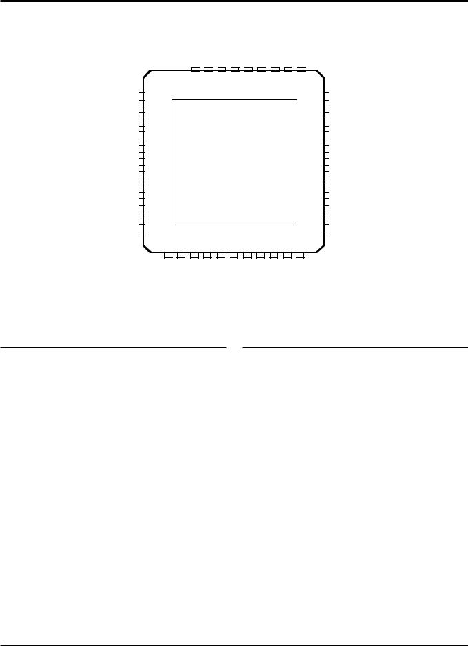
44-Lead PLCC Pin Assignments
44-Lead PLCC Pin Identification
Pin # |
Symbol |
Function |
Direction |
|
|
|
|
1 |
VCC |
Power Supply |
Input |
2 |
XTAL2 |
Crystal, Oscillator Clock |
Output |
3 |
XTAL1 |
Crystal, Oscillator Clock |
Input |
4 |
P37 |
Port 3 pin 7 |
Output |
|
|
|
|
5 |
P30 |
Port 3 pin 0 |
Input |
6 |
N/C |
Not Connected |
Input |
7 |
/RESET |
Reset |
Input |
8 |
R//W |
Read/Write |
Output |
|
|
|
|
9 |
/DS |
Data Strobe |
Output |
10 |
/AS |
Address Strobe |
Output |
11 |
P35 |
Port 3 pin 5 |
Output |
12 |
GND |
Ground, GND |
Input |
13 |
P32 |
Port 3 pin 2 |
Input |
|
|
|
|
Pin # |
Symbol |
Function |
Direction |
|
|
|
|
14-16 |
P00-P02 |
Port 0 pin 0,1,2 |
In/Output |
17 |
R//RL |
ROM/ROMless control |
Input |
18-22 |
P03-P07 |
Port 0 pin 3,4,5,6,7 |
In/Output |
23-27 |
P10-P14 |
Port 1 pin 0,1,2,3,4 |
In/Output |
|
|
|
|
28 |
N/C |
Not Connected |
Input |
29-31 |
P15-P17 |
Port 1 pin 5,6,7 |
In/Output |
32 |
P34 |
Port 3 pin 4 |
Output |
33 |
P33 |
Port 3 pin 3 |
Input |
|
|
|
|
34-38 |
P20-P24 |
Port 2 pin 0,1,2,3,4 |
In/Output |
39 |
N/C |
Not Connected |
Input |
40-42 |
P25-P27 |
Port 2 pin 5,6,7 |
In/Output |
43 |
P31 |
Port 3 pin 1 |
Input |
44 |
P36 |
Port 3 pin 6 |
Output |
|
|
|
|
4
 Loading...