


ZILOG Z86C0412PSC, Z86C0412SAC, Z86C0412SEC, Z86C0412SSC, Z86C0412PAC Datasheet
...PRELIMINARY PRODUCT SPECIFICATION
1
Z86C04/C08 1
CMOS 8-BIT LOW-COST
1K/2K-ROM MICROCONTROLLERS
FEATURES
Part |
ROM |
RAM* |
Speed |
Auto |
Permanent |
Number |
(KB) |
(Bytes) |
(MHz) |
Latch |
WDT |
|
|
|
|
|
|
Z86C04 |
1 |
125 |
12 |
Optional |
Optional |
Z86C08 |
2 |
125 |
12 |
Optional |
Optional |
|
|
|
|
|
|
Note: * General-Purpose
■18-Pin DIP and SOIC Packages
■3.0V to 5.5V Operating Range
■Available Temperature Ranges A = –40°C to +125°C
E = –40°C to +105°C S = 0°C to +70°C
■14 Input / Output Lines
■Six Vectored, Prioritized Interrupts from Six Different Sources
■Two On-Board Comparators
■ROM Mask Options:
–Low Noise
–ROM Protect
–Auto Latch
–System Clock Driving WDT (Z86C04 only)
–Permanent Watch-Dog Timer (WDT)
–RC Oscillator
–32 kHz Operation
■Two Programmable 8-Bit Counter/Timers, Each with 6-Bit Programmable Prescaler
■Power-On Reset (POR) Timer
■On-Chip Oscillator that Accepts RC, Crystal, Ceramic Resonance, LC, or External Clock Drive
■Clock-Free WDT Reset
■Low-Power Consumption (50mw)
■Fast Instruction Pointer (1.0 s @ 12 MHz)
■Fourteen Digital Inputs at CMOS Levels; Schmitt-Triggered
■Software Enabled Watch-Dog Timer
■Programmable Interrupt Polarity
■Two Standby Modes: STOP and HALT
■Low-Voltage Protection
GENERAL DESCRIPTION
Zilog’s Z86C04/C08 are members of the Z8® MCU singlechip microcontroller family which offer easy software/hardware system expansion.
For applications demanding powerful I/O capabilities, the Z86C04/C08’s dedicated input and output lines are grouped into three ports, and are configurable under software control to provide timing, status signals, or parallel I/O.
Two on-chip counter/timers, with a large number of user selectable modes, off-load the system of administering real-time tasks such as counting/timing and I/O data communications. Additionally, two on-board comparators process analog signals with a common reference voltage (Figure 1).
DS97DZ80502 |
P R E L I M I N A R Y |
1 |

Z86C04/C08 |
|
CMOS 8-Bit Low-Cost 1K/2K-ROM Microcontrollers |
Zilog |
GENERAL DESCRIPTION (Continued)
Note: All Signals with a preceding front slash, "/", are active Low, e.g.: B//W (WORD is active Low); /B/W (BYTE is active Low, only).
Power connections follow conventional descriptions below:
Connection |
Circuit |
Device |
Power |
VCC |
VDD |
Ground |
GND |
VSS |
Input |
Vcc |
GND |
XTAL |
|
|
|
|
|
|
|
|
|
|
|
|
|
|
|
|
|
|
|
|
|
|
|
|
|
|
|
|
|
|
|
|
|
|
|
|
|
|
|
|
|
|
|
|
|
|
|
|
|
|
|
|
|
|
|
|
|
|
|
|
|
|
|
|
|
|
|
|
|
|
|
|
|
|
|
|
|
|
|
|
|
|
|
|
Port 3 |
|
|
|
|
|
|
|
|
|
|
|
|
|
|
|
|
|
Machine |
|||||||||
|
|
|
|
|
|
|
|
|
|
|
|
|
|
|
|
||||||||||||
|
|
|
|
|
|
|
|
|
|
|
|
|
|
|
|
|
Timing & Inst. |
||||||||||
|
|
|
|
|
|
|
|
|
|
|
|
|
|
|
|
|
|
|
|
|
|
|
|||||
|
|
|
|
|
|
|
|
|
|
|
|
|
|
|
|
|
|
|
|
|
|
|
Control |
||||
|
|
|
|
|
|
|
|
|
|
|
|
|
|
|
|
|
|
|
|
|
|
||||||
|
|
|
|
|
|
|
|
|
|
|
|
|
|
|
|
|
|
|
|
|
|
|
|
|
|
|
|
|
|
|
|
|
|
|
|
|
|
|
|
|
|
|
|
|
|
|
|
|
|
|
|
|
|
|
|
Counter/ |
|
|
|
|
|
ALU |
|
|
|
|
|
|
|
|
|
|
|
||||||||||
|
|
|
|
|
|
|
|
|
|
|
|
|
|
|
|
||||||||||||
Timers (2) |
|
|
|
|
|
|
|
|
|
|
|
|
|
|
|
|
|||||||||||
|
|
|
|
|
|
|
|
|
|
|
|
|
|
|
|
|
|
|
|
|
|
||||||
|
|
|
|
|
|
|
|
|
|
|
|
|
|
|
|
|
|
|
|
|
|
|
|
|
|
|
|
|
|
|
|
|
|
|
|
|
|
|
FLAG |
|
|
|
|
|
|
|
|
|
|
|
|||||
Interrupt |
|
|
|
|
|
|
|
|
|
|
Prg. Memory |
||||||||||||||||
|
|
|
|
|
|
|
|
|
|
|
|
|
|
|
|
|
|||||||||||
|
|
|
|
|
|
|
|
|
|
|
|
|
|
|
|
|
|||||||||||
Control |
|
|
|
|
|
|
|
|
|
|
|
|
|
|
|
|
|
||||||||||
|
|
|
|
|
|
|
|
|
|
|
|
|
|
|
|
|
|||||||||||
|
|
|
|
|
|
|
|
|
|
|
|
|
|
|
|
|
|
|
|
|
|
||||||
|
|
|
|
|
|
|
|
|
|
|
|
|
|
|
|
|
|
|
|
|
|
|
|
|
|||
|
|
|
|
|
|
|
|
|
|
|
Register |
|
|
|
|
|
|
|
|
|
|
|
|||||
|
|
|
|
|
|
|
|
|
|
|
|
|
|
|
|
|
|
|
|
|
|||||||
Two Analog |
|
|
|
|
|
Pointer |
|
|
|
|
|
|
|
|
|
|
|
||||||||||
|
|
|
|
|
|
|
|
|
|
|
|
|
|
|
|
|
Program |
||||||||||
Comparators |
|
|
|
|
|
|
|
|
|
|
|
|
|
|
|
|
|
||||||||||
|
|
|
|
|
|
|
|
|
|
|
|
|
|
|
|
|
|||||||||||
|
|
|
|
Register File |
|
|
|
|
|
|
Counter |
||||||||||||||||
|
|
|
|
|
|
|
|
|
|
|
|
|
|
|
|
||||||||||||
|
|
|
|
|
|
|
|
|
|
|
|
|
|
|
|
|
|
|
|
|
|||||||
|
|
|
|
|
|
|
|
|
|
|
|
|
|
|
|
|
|
|
|
|
|
|
|
|
|
|
|
|
|
|
|
|
|
|
|
|
|
|
|
|
|
|
|
|
|
|
|
|
|
|
|
|
|
|
|
|
|
|
|
|
|
|
|
|
|
|
|
|
|
|
|
|
|
|
|
|
|
|
|
|
|
|
|
|
|
|
|
|
|
|
|
|
|
|
|
|
|
|
|
|
|
|
|
|
|
|
|
|
|
|
|
|
|
|
|
|
|
|
|
|
|
|
|
|
|
|
|
|
|
|
|
|
|
|
|
|
|
|
|
|
|
|
|
|
|
|
|
|
|
|
|
|
|
|
|
|
|
|
|
|
|
|
|
|
|
|
|
Port 2 |
|
Port 0 |
|
|
|
I/O |
I/O |
(Bit Programmable) |
|
Figure 1. Z86C04/C08
Functional Block Diagram
2 |
P R E L I M I N A R Y |
DS97DZ80502 |

|
Z86C04/C08 |
Zilog |
CMOS 8-Bit Low-Cost 1K/2K-ROM Microcontrollers |
|
|
PIN DESCRIPTIONS
P24 |
|
|
1 |
18 |
|
P23 |
|
|
|
||||
|
|
2 |
17 |
|
|
|
P25 |
|
|
|
P22 |
||
|
|
3 |
|
|
|
|
P26 |
|
|
16 |
|
P21 |
|
|
|
4 |
|
|
|
|
P27 |
|
|
15 |
|
P20 |
|
|
|
|||||
|
|
5 |
DIP 14 |
|
|
|
VCC |
|
|
|
GND |
||
|
|
6 |
|
|
|
|
XTAL2 |
|
|
13 |
|
P02 |
|
|
|
|||||
|
|
7 |
|
|
|
|
XTAL1 |
|
|
12 |
|
P01 |
|
|
|
8 |
|
|
|
|
P31 |
|
|
11 |
|
P00 |
|
|
|
|
||||
|
|
9 |
|
|
|
|
P32 |
|
|
10 |
|
P33 |
|
|
|
|
|
|||
Figure 2. |
18-Pin DIP Configuration |
|||||
Table 1: 18-Pin DIP and SOIC Pin Identification
Pin # |
Symbol |
Function |
Direction |
|
|
|
|
1-4 |
P24-P27 |
Port 2, Pins 4, 5, 6, 7 |
In/Output |
5 |
V CC |
Power Supply |
|
6 |
XTAL2 |
Crystal Oscillator Clock |
Output |
7 |
XTAL1 |
Crystal Oscillator Clock |
Input |
8 |
P31 |
Port 3, Pin 1, AN1 |
Input |
9 |
P32 |
Port 3, Pin 2, AN2 |
Input |
10 |
P33 |
Port 3, Pin 3, REF |
Input |
11-13 |
P00-P02 |
Port 0, Pins 0, 1, 2 |
In/Output |
14 |
GND |
Ground |
|
15-18 |
P20-P23 |
Port 2, Pins 0, 1, 2, 3 |
In/Output |
|
|
|
|
P24 |
|
|
|
1 |
|
18 |
|
|
|
P23 |
|
|
|
|
|
|
|
||||
P25 |
|
2 |
|
17 |
|
|
|
P22 |
||
|
|
|
|
|
|
|
||||
P26 |
|
3 |
|
16 |
|
|
|
P21 |
||
|
|
|
|
|
|
|
||||
P27 |
|
|
|
4 |
|
15 |
|
|
|
P20 |
|
|
|
|
|
||||||
|
|
|
|
|
|
|
||||
Vcc |
|
5 |
SOIC |
14 |
|
|
|
GND |
||
|
|
|
|
|
|
|||||
XTAL2 |
|
6 |
|
13 |
|
|
|
P02 |
||
|
|
|
|
|
|
|
||||
XTAL1 |
|
7 |
|
12 |
|
|
|
P01 |
||
|
|
|
|
|
|
|
||||
P31 |
|
|
|
8 |
|
11 |
|
|
|
P00 |
|
|
|
|
|
||||||
|
|
|
|
|
|
|
||||
P32 |
|
9 |
|
10 |
|
|
|
P33 |
||
|
|
|
|
|
|
|
||||
|
|
|
|
|
|
|
|
|
|
|
Figure 3. 18-Pin SOIC Pin Configuration
DS97DZ80502 |
P R E L I M I N A R Y |
3 |
Z86C04/C08 |
|
CMOS 8-Bit Low-Cost 1K/2K-ROM Microcontrollers |
Zilog |
ABSOLUTE MAXIMUM RATINGS
Parameter |
|
Min |
Max |
Units |
|
|
|
|
|
Ambient Temperature under Bias |
|
–40 |
+105 |
C |
Storage Temperature |
|
–65 |
+150 |
C |
Voltage on any Pin with Respect to V [Note 1] |
–0.7 |
+12 |
V |
|
|
SS |
|
|
|
Voltage on V Pin with Respect to V |
SS |
–0.3 |
+7 |
V |
DD |
|
|
|
|
Voltage on Pin 7 with Respect to VSS [Note 2] |
–0.7 |
VDD+1 |
V |
|
Total Power Dissipation |
|
|
462 |
mW |
Maximum Current out of V |
|
|
84 |
mA |
SS |
|
|
|
|
Maximum Current into V |
|
|
84 |
mA |
DD |
|
|
|
|
Maximum Current into an Input Pin [Note 3] |
–600 |
+600 |
A |
|
Maximum Current into an Open-Drain Pin [Note 4] |
–600 |
+600 |
A |
|
Maximum Output Current Sinked by Any I/O Pin |
|
12 |
mA |
|
Maximum Output Current Sourced by Any I/O Pin |
|
12 |
mA |
|
Total Maximum Output Current Sinked by Port 2 |
|
70 |
mA |
|
Total Maximum Output Current Sourced by Port 2 |
|
70 |
mA |
|
|
|
|
|
|
Notes:
1.This applies to all pins except where otherwise noted. Maximum current into pin must be ±600 A.
2.There is no input protection diode from pin to VDD.
3.This excludes Pin 6 and Pin 7.
4.Device pin is not at an output Low state.
Stresses greater than those listed under Absolute Maximum Ratings may cause permanent damage to the device. This is a stress rating only; functional operation of the device at any condition above those indicated in the operational sections of these specifications is not implied. Exposure to absolute maximum rating conditions for an ex-
tended period may affect device reliability. Total power
dissipation should not exceed 462 |
mW for the package. |
||||
Power dissipation is calculated as follows: |
|||||
Total Power dissipation = VDD x [I |
– (sum of I )] + sum of |
||||
[(V |
– V ) x I |
] + sum of (V |
|
DD |
OH |
x I ). |
|
||||
DD |
OH |
OH |
0L |
0L |
|
STANDARD TEST CONDITIONS
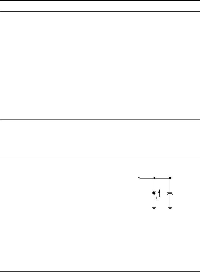
The characteristics listed below apply for standard test conditions as noted. All voltages are referenced to Ground. Positive current flows into the referenced pin (Figure 4).
From Output
Under Test
150 pF
Figure 4. Test Load Diagram
4 |
P R E L I M I N A R Y |
DS97DZ80502 |

|
Z86C04/C08 |
Zilog |
CMOS 8-Bit Low-Cost 1K/2K-ROM Microcontrollers |
|
|
CAPACITANCE
TA = 25°C, VCC = GND = 0V, f = 1.0 MHz, unmeasured pins returned to GND.
Parameter |
Min |
Max |
|
|
|
Input capacitance |
0 |
15 pF |
|
|
|
Output capacitance |
0 |
20 pF |
|
|
|
I/O capacitance |
0 |
25 pF |
|
|
|
DC ELECTRICAL CHARACTERISTICS
|
|
|
|
TA = –40°C |
Typical |
|
|
|
|
|
|
|
||
|
|
|
|
to +125°C |
|
|
|
|
|
|
|
|||
Sym |
Parameter |
VCC [4] |
|
Min |
|
Max |
@ 25°C |
Units |
|
Conditions |
Notes |
|||
|
|
|
|
|
|
|
|
|
|
|||||
VCH |
Clock Input High |
3.0V |
0.8 V |
V |
+0.3 |
1.7 |
V |
Driven by External |
|
|||||
|
Voltage |
|
|
CC |
|
CC |
|
|
Clock Generator |
|
|
|||
|
|
|
|
|
|
|
|
|
|
|||||
|
|
|
|
|
|
|
|
|
|
|||||
|
|
5.5V |
0.8 V |
V |
+0.3 |
2.8 |
V |
Driven by External |
|
|||||
|
|
|
|
CC |
|
CC |
|
|
Clock Generator |
|
|
|||
|
|
|
|
|
|
|
|
|
|
|
||||
|
|
|
|
|
|
|
|
|
|
|||||
VCL |
Clock Input Low |
3.0V |
V |
–0.3 |
0.2 V |
0.8 |
V |
Driven by External |
|
|||||
|
Voltage |
|
|
SS |
|
CC |
|
|
Clock Generator |
|
|
|||
|
|
|
|
|
|
|
|
|
|
|||||
|
|
|
|
|
|
|
|
|
|
|||||
|
|
5.5V |
V |
–0.3 |
0.2 V |
1.7 |
V |
Driven by External |
|
|||||
|
|
|
|
SS |
|
CC |
|
|
|
|
|
|
|
|
|
|
|
|
|
|
|
|
Clock Generator |
|
|
||||
|
|
|
|
|
|
|
|
|
|
|
||||
|
|
|
|
|
|
|
|
|
|
|
|
|
|
|
V |
Input High Voltage |
3.0V |
0.7 V |
V |
+0.3 |
1.8 |
V |
|
|
|
|
|
1 |
|
IH |
|
|
|
CC |
|
CC |
|
|
|
|
|
|
|
|
|
|
5.5V |
0.7 V |
V |
+0.3 |
2.8 |
V |
|
|
|
|
|
1 |
|
|
|
|
|
CC |
|
CC |
|
|
|
|
|
|
|
|
V |
Input Low Voltage |
3.0V |
V |
–0.3 |
0.2 V |
0.8 |
V |
|
|
|
|
|
1 |
|
IL |
|
|
|
SS |
|
CC |
|
|
|
|
|
|
|
|
|
|
5.5V |
V |
–0.3 |
0.2 V |
1.5 |
V |
|
|
|
|
|
1 |
|
|
|
|
|
SS |
|
CC |
|
|
|
|
|
|
|
|
V |
Output High |
3.0V |
V |
–0.4 |
|
|
3.0 |
V |
I |
= –2.0 mA |
|
5 |
||
OH |
Voltage |
|
CC |
|
|
|
|
OH |
|
|
|
|
|
|
|
5.5V |
V |
–0.4 |
|
|
4.8 |
V |
I |
= –2.0 mA |
|
5 |
|||
|
|
|
|
|
||||||||||
|
|
|
CC |
|
|
|
|
OH |
|
|
|
|
|
|
|
|
3.0V |
V |
–0.4 |
|
|
3.0 |
V |
Low Noise @ I |
= –0.5 mA |
|
|||
|
|
|
CC |
|
|
|
|
|
|
|
OH |
|
|
|
|
|
5.5V |
V |
–0.4 |
|
|
4.8 |
V |
Low Noise @ I |
= –0.5 mA |
|
|||
|
|
|
CC |
|
|
|
|
|
|
|
OH |
|
|
|
V |
Output Low Voltage |
3.0V |
|
|
|
0.8 |
0.2 |
V |
I |
= +4.0 mA |
|
5 |
||
OL1 |
|
|
|
|
|
|
|
|
OL |
|
|
|
|
|
|
|
5.5V |
|
|
|
0.6 |
0.1 |
V |
I |
= +4.0 mA |
|
5 |
||
|
|
|
|
|
|
|
|
|
OL |
|
|
|
|
|
|
|
3.0V |
|
|
|
0.6 |
0.2 |
V |
Low Noise @ I |
= 1.0 mA |
|
|||
|
|
|
|
|
|
|
|
|
|
|
|
OL |
|
|
|
|
5.5V |
|
|
|
0.6 |
0.1 |
V |
Low Noise @ I |
= 1.0 mA |
|
|||
|
|
|
|
|
|
|
|
|
|
|
|
OL |
|
|
V |
Output Low Voltage |
3.0V |
|
|
|
1.2 |
0.8 |
V |
I |
= +12 mA |
|
5 |
||
OL2 |
|
|
|
|
|
|
|
|
OL |
|
|
|
|
|
|
|
5.5V |
|
|
|
1.0 |
0.3 |
V |
I |
= +12 mA |
|
5 |
||
|
|
|
|
|
|
|
|
|
OL |
|
|
|
|
|
V |
Comparator Input |
3.0V |
|
|
|
25 |
10 |
mV |
|
|
|
|
|
|
OFFSET |
Offset Voltage |
|
|
|
|
|
|
|
|
|
|
|
|
|
|
5.5V |
|
|
|
25 |
10 |
mV |
|
|
|
|
|
|
|
|
|
|
|
|
|
|
|
|
|
|||||
VLV |
VCC Low Voltage |
|
|
1.8 |
|
3.0 |
2.6 |
V Int. CLK Freq @ 2 MHz Max. |
|
|||||
|
Auto Reset |
|
|
|
|
|
|
|
|
|
|
|
|
|
|
|
|
|
|
|
|
|
|
|
|
|
|
|
|
I |
Input Leakage |
3.0V |
|
–1.0 |
|
1.0 |
|
A |
V |
= 0V, V |
CC |
|
|
|
IL |
(Input Bias |
|
|
|
|
|
|
|
IN |
|
|
|
||
|
5.5 |
|
–1.0 |
|
1.0 |
|
A |
VIN = 0V, VCC |
|
|
||||
|
Current of |
|
|
|
|
|
||||||||
|
|
|
|
|
|
|
|
|
|
|
|
|
|
|
|
Comparator) |
|
|
|
|
|
|
|
|
|
|
|
|
|
|
|
|
|
|
|
|
|
|
|
|
|
|
|
|
I |
Output Leakage |
3.0V |
|
–1.0 |
|
1.0 |
|
A |
V |
= 0V, V |
CC |
|
|
|
OL |
|
|
|
|
|
|
|
|
IN |
|
|
|
|
|
|
|
5.5V |
|
–1.0 |
|
1.0 |
|
A |
VIN = 0V, Vcc |
|
|
|||
DS97DZ80502 |
P R E L I M I N A R Y |
5 |

Z86C04/C08 |
|
|
|
|
|
|
|
|
|
|
CMOS 8-Bit Low-Cost 1K/2K-ROM Microcontrollers |
|
|
|
|
Zilog |
|||||
|
|
|
|
|
|
|||||
DC ELECTRICAL CHARACTERISTICS (Continued) |
|
|
|
|
|
|||||
|
|
|
|
|
|
|
|
|
|
|
V |
Comparator Input |
|
0 |
V –1.5 |
|
V |
|
|
|
|
VICR |
Common Mode |
|
|
CC |
|
|
|
|
|
|
|
|
|
|
|
|
|
|
|
|
|
|
Voltage Range |
|
|
|
|
|
|
|
|
|
|
|
|
|
|
|
|
|
|
|
|
ICC |
Supply Current |
3.0V |
|
3.5 |
1.5 |
mA |
All Output and I/O Pins Floating |
5,7 |
|
|
|
|
|
|
|
|
|
@ 2 MHz |
|
|
|
|
|
|
|
|
|
|
|
|
|
|
|
|
5.5V |
|
7.0 |
3.8 |
mA |
All Output and I/O Pins Floating |
5,7 |
|
|
|
|
|
|
|
|
|
@ 2 MHz |
|
|
|
|
|
|
|
|
|
|
|
|
|
|
|
|
3.0V |
|
8.0 |
3.0 |
mA |
All Output and I/O Pins Floating |
5,7 |
|
|
|
|
|
|
|
|
|
@ 8 MHz |
|
|
|
|
|
|
|
|
|
|
|
|
|
|
|
|
5.5V |
|
11.0 |
4.4 |
mA |
All Output and I/O Pins Floating |
5,7 |
|
|
|
|
|
|
|
|
|
@ 8 MHz |
|
|
|
|
|
|
|
|
|
|
|
|
|
|
|
|
3.0V |
|
10 |
3.6 |
mA |
All Output and I/O Pins Floating |
5,7 |
|
|
|
|
|
|
|
|
|
@ 12 MHz |
|
|
|
|
|
|
|
|
|
|
|
|
|
|
|
|
5.5V |
|
15 |
9.0 |
mA |
All Output and I/O Pins Floating |
5,7 |
|
|
|
|
|
|
|
|
|
@ 12 MHz |
|
|
|
|
|
|
|
|
|
|
|
|
|
|
I |
Standby Current |
3.0V |
|
2.5 |
0.7 |
mA |
HALT mode VIN = 0V, |
5,7 |
|
|
CC1 |
|
|
|
|
|
|
V |
@ 2 MHz |
|
|
|
|
|
|
|
|
|
|
|
||
|
|
|
|
|
|
|
|
CC |
|
|
|
|
5.5V |
|
4.0 |
2.5 |
mA |
HALT mode VIN = 0V, |
5,7 |
|
|
|
|
|
|
|
|
|
V |
@ 2 MHz |
|
|
|
|
|
|
|
|
|
|
CC |
|
|
|
|
3.0V |
|
4.0 |
1.0 |
mA |
HALT mode VIN = 0V, |
5,7 |
|
|
|
|
|
|
|
|
|
V |
@ 8 MHz |
|
|
|
|
|
|
|
|
|
|
CC |
|
|
|
|
5.5V |
|
5.0 |
3.0 |
mA |
HALT mode VIN = 0V, |
5,7 |
|
|
|
|
|
|
|
|
|
V |
@ 8 MHz |
|
|
|
|
|
|
|
|
|
|
CC |
|
|
|
|
3.0V |
|
4.5 |
1.5 |
mA |
HALT mode VIN = 0V, |
5,7 |
|
|
|
|
|
|
|
|
|
V |
@ 12 MHz |
|
|
|
|
|
|
|
|
|
|
CC |
|
|
|
|
5.5V |
|
7.0 |
4.0 |
mA |
HALT mode VIN = 0V, |
5,7 |
|
|
|
|
|
|
|
|
|
V |
@ 12 MHz |
|
|
|
|
|
|
|
|
|
|
CC |
|
|
I |
Supply Current |
3.0V |
|
3.5 |
1.5 |
mA |
All Output and I/O Pins Floating |
7 |
|
|
CC |
(Low Noise Mode) |
|
|
|
|
|
@ 1 MHz |
|
|
|
|
|
|
|
|
|
|
|
|||
|
|
|
|
|
|
|
|
|
|
|
|
|
5.5V |
|
7.0 |
3.8 |
mA |
All Output and I/O Pins Floating |
7 |
|
|
|
|
|
|
|
|
|
@ 1 MHz |
|
|
|
|
|
|
|
|
|
|
|
|
|
|
|
|
3.0V |
|
5.8 |
2.5 |
mA |
All Output and I/O Pins Floating |
7 |
|
|
|
|
|
|
|
|
|
@ 2 MHz |
|
|
|
|
|
|
|
|
|
|
|
|
|
|
|
|
5.5V |
|
9.0 |
4.0 |
mA |
All Output and I/O Pins Floating |
7 |
|
|
|
|
|
|
|
|
|
@ 2 MHz |
|
|
|
|
|
|
|
|
|
|
|
|
|
|
|
|
3.0V |
|
8.0 |
3.0 |
mA |
All Output and I/O Pins Floating |
7 |
|
|
|
|
|
|
|
|
|
@ 4 MHz |
|
|
|
|
|
|
|
|
|
|
|
|
|
|
|
|
5.5V |
|
11.0 |
4.4 |
mA |
All Output and I/O Pins Floating |
7 |
|
|
|
|
|
|
|
|
|
@ 4 MHz |
|
|
|
|
|
|
|
|
|
|
|
|
|
|
6 |
P R E L I M I N A R Y |
DS97DZ80502 |

Z86C04/C08 |
|
CMOS 8-Bit Low-Cost 1K/2K-ROM Microcontrollers |
Zilog |
DC ELECTRICAL CHARACTERISTICS (Continued)
|
|
|
|
|
|
|
|
|
|
|
|
TA = –40°C |
Typical |
|
|
|
|
|
|
|
to +125°C |
|
|
|
|
|
Sym |
Parameter |
VCC [4] |
Min Max |
@ 25°C Units |
Conditions |
Notes |
||
|
|
|
|
|
|
|
|
|
I |
Standby Current |
3.0V |
2.5 |
0.7 |
mA |
HALT mode VIN = 0V, V |
@ 1MHz |
7 |
CC1 |
(Low Noise Mode) |
|
|
|
|
CC |
|
|
|
5.5V |
4.0 |
2.5 |
mA |
HALT mode VIN = 0V, VCC @ 1MHz |
|
||
|
|
|
||||||
|
|
3.0V |
3.0 |
0.9 |
mA |
HALT mode VIN = 0V, VCC @ 2 MHz |
7 |
|
|
|
5.5V |
4.5 |
2.8 |
mA |
HALT mode VIN = 0V, VCC @ 2 MHz |
7 |
|
|
|
3.0V |
4.0 |
1.0 |
mA |
HALT mode VIN = 0V, VCC @ 4 MHz |
7 |
|
|
|
5.5V |
5.0 |
3.0 |
mA |
HALT mode VIN = 0V, VCC @ 4 MHz |
7 |
|
I |
Standby Current |
3.0V |
20 |
1.0 |
A |
STOP mode VIN = 0V, V |
;WDT is not |
7 |
CC2 |
|
|
|
|
|
Running |
CC |
|
|
|
|
|
|
|
|
|
|
|
|
|
|
|
|
|
|
|
|
|
5.5V |
20 |
1.0 |
A |
STOP mode VIN = 0V, VCC ;WDTis not |
7 |
|
|
|
|
|
|
|
Running |
|
|
|
|
|
|
|
|
|
|
|
IALL |
Auto Latch Low Current |
3.0V |
8.0 |
3.0 |
A |
0V < VIN < VCC |
|
|
|
|
5.5V |
30 |
16 |
A |
0V < VIN < VCC |
|
|
IALH |
Auto Latch High Current |
3.0V |
–5.0 |
–1.5 |
A |
0V < VIN < VCC |
|
|
|
|
5.5V |
–20 |
–8.0 |
A |
0V < VIN < VCC |
|
|
Notes:
1.Port 0, 2, and 3 only.
2.VSS = 0V = GND.
3.The device operates down to VLV. The minimum operational VCC is determined on the value of the voltage VLV at the ambient temperature. The VLV increases as the temperature decreases.
4.VCC = 3.0V to 5.5V, typical values measured at VCC = 3.3V and VCC = 5.0V.
5.Standard Mode (not Low EMI mode).
6.Z86C08 only.
7.Inputs at power rail and outputs are unloaded.
7 |
P R E L I M I N A R Y |
DS97DZ80502 |

Z86C04/C08 |
|
|
|
|
|
|
|
|
|
|
|
CMOS 8-Bit Low-Cost 1K/2K-ROM Microcontrollers |
|
|
|
|
|
Zilog |
|||||
|
|
|
|
|
|
|
|||||
DC ELECTRICAL CHARACTERISTICS (Continued) |
|
|
|
|
|
|
|||||
|
|
|
|
|
|
|
|
|
|
||
|
|
|
TA= 0°C to |
TA= –40°C to |
Typical |
|
|
|
|
||
|
|
|
+70°C |
+105°C |
|
|
|
|
|||
|
|
|
|
|
|
|
|
||||
Symbol |
Parameter |
VCC |
Min |
Max |
Min |
Max |
@ 25°C Units |
Conditions |
Notes |
||
VCH |
Clock Input High |
3.0V |
0.8 VCC VCC+0.3 |
0.8 VCC VCC+0.3 |
1.7 |
V |
Driven by External |
|
|
||
|
Voltage |
|
|
|
|
|
|
|
Clock Generator |
|
|
|
|
|
|
|
|
|
|
|
|
||
|
|
5.5V |
0.8 VCC VCC+0.3 |
0.8 VCC VCC+0.3 |
2.8 |
V |
Driven by External |
|
|
||
|
|
|
|
|
|
|
|
|
Clock Generator |
|
|
VCL |
Clock Input Low |
3.0V |
VSS–0.3 |
0.2 VCC |
VSS–0.3 0.2 VCC |
0.8 |
V |
Driven by External |
|
|
|
|
Voltage |
|
|
|
|
|
|
|
Clock Generator |
|
|
|
|
|
|
|
|
|
|
|
|
|
|
|
|
5.5V |
VSS–0.3 |
0.2 VCC |
VSS–0.3 0.2 VCC |
1.7 |
V |
Driven by External |
|
|
|
|
|
|
|
|
|
|
|
|
Clock Generator |
|
|
|
|
|
|
|
|
|
|
|
|||
V |
Input High Voltage |
3.0V |
0.7 VCC VCC+0.3 0.7 VCC VCC+0.3 |
1.8 |
V |
|
1 |
|
|||
IH |
|
|
|
|
|
|
|
|
|
|
|
|
|
5.5V |
0.7 VCC VCC+0.3 0.7 VCC VCC+0.3 |
2.8 |
V |
|
1 |
|
|||
V |
Input Low Voltage |
3.0V |
VSS–0.3 |
0.2 VCC |
VSS–0.3 0.2 VCC |
0.8 |
V |
|
1 |
|
|
IL |
|
|
|
|
|
|
|
|
|
|
|
|
|
5.5V |
VSS–0.3 |
0.2 VCC |
VSS–0.3 0.2 VCC |
1.5 |
V |
|
1 |
|
|
V |
Output High Voltage |
3.0V |
VCC–0.4 |
|
VCC–0.4 |
|
3.0 |
V |
IOH = –2.0 mA |
5 |
|
OH |
|
|
|
|
|
|
|
|
|
|
|
|
|
5.5V |
VCC–0.4 |
|
VCC–0.4 |
|
4.8 |
V |
IOH = –2.0 mA |
5 |
|
|
|
3.0V |
VCC–0.4 |
|
VCC–0.4 |
|
3.0 |
V |
Low Noise @ |
|
|
|
|
|
|
|
|
|
|
|
IOH = –0.5 mA |
|
|
|
|
5.5V |
VCC–0.4 |
|
VCC–0.4 |
|
4.8 |
V |
Low Noise @ |
|
|
|
|
|
|
|
|
|
|
|
IOH = –0.5 mA |
|
|
V |
Output Low Voltage |
3.0V |
|
0.8 |
|
0.8 |
0.2 |
V |
IOL= +4.0 mA |
5 |
|
OL1 |
|
|
|
|
|
|
|
|
|
|
|
|
|
5.5V |
|
0.4 |
|
0.4 |
0.1 |
V |
IOL= +4.0 mA |
5 |
|
|
|
3.0V |
|
0.4 |
|
0.4 |
0.2 |
V |
Low Noise @ |
|
|
|
|
|
|
|
|
|
|
|
IOL = 1.0 mA |
|
|
|
|
5.5V |
|
0.4 |
|
0.4 |
0.1 |
V |
Low Noise @ |
|
|
|
|
|
|
|
|
|
|
|
IOL = 1.0 mA |
|
|
V |
Output Low Voltage |
3.0V |
|
1.0 |
|
1.0 |
0.8 |
V |
IOL = +12 mA |
5 |
|
OL2 |
|
|
|
|
|
|
|
|
|
|
|
|
|
5.5V |
|
0.8 |
|
0.8 |
0.3 |
V |
IOL = +12 mA |
5 |
|
V |
Comparator Input |
3.0V |
|
25 |
|
25 |
10 |
mV |
|
|
|
OFFSET |
Offset Voltage |
|
|
|
|
|
|
|
|
|
|
|
5.5V |
|
25 |
|
25 |
10 |
mV |
|
|
|
|
|
|
|
|
|
|
|
|
|
|
|
|
VLV |
VCC Low Voltage |
|
2.2 |
2.8 |
|
|
2.6 |
V |
Int. CLK Freq @ |
|
|
|
Auto Reset |
|
|
|
|
|
|
|
6 MHz Max. |
|
|
|
|
|
|
|
2.0 |
3.0 |
2.6 |
V |
Int. CLK Freq @ |
|
|
|
|
|
|
|
|
|
|
|
4 MHz Max. |
|
|
|
|
|
|
|
|
|
|
|
|
|
|
IIL |
Input Leakage |
3.0V |
–1.0 |
1.0 |
–1.0 |
1.0 |
|
A |
VIN = 0V, VCC |
|
|
|
(Input Bias Current |
|
|
|
|
|
|
|
|
|
|
|
5.5V |
–1.0 |
1.0 |
–1.0 |
1.0 |
|
A |
VIN = 0V, VCC |
|
|
|
|
of Comparator) |
|
|
|
|
|
|
|
|
|
|
I |
Output Leakage |
3.0V |
–1.0 |
1.0 |
–1.0 |
1.0 |
|
A |
VIN = 0V, VCC |
|
|
OL |
|
|
|
|
|
|
|
|
|
|
|
|
|
5.5V |
–1.0 |
1.0 |
–1.0 |
1.0 |
|
A |
VIN = 0V, VCC |
|
|
V |
Comparator Input |
|
0 |
VCC–1.0 |
0 |
VCC–1.5 |
|
V |
|
|
|
VICR
Common Mode
Voltage Range
8 |
P R E L I M I N A R Y |
DS97DZ80502 |

Z86C04/C08 |
|
|
|
|
|
|
|
|
|
|
|
CMOS 8-Bit Low-Cost 1K/2K-ROM Microcontrollers |
|
|
|
|
|
Zilog |
|||||
|
|
|
|
|
|
|
|||||
DC ELECTRICAL CHARACTERISTICS (Continued) |
|
|
|
|
|
|
|||||
|
|
|
|
|
|
|
|
|
|
|
|
|
|
|
TA= 0°C to |
TA= –40°C to |
Typical |
|
|
|
|
|
|
|
|
|
+70°C |
+105°C |
|
|
|
|
|
||
|
|
|
|
|
|
|
|
|
|||
Symbol |
Parameter |
VCC |
Min |
Max |
Min Max |
@ 25°C Units |
|
Conditions |
Notes |
||
Icc |
Supply Current |
3.0V |
|
3.5 |
3.5 |
1.5 |
mA |
All Output and I/O |
5,7 |
|
|
|
|
|
|
|
|
|
|
Pins Floating @ |
|
|
|
|
|
|
|
|
|
|
|
2 MHz |
|
|
|
|
|
|
|
|
|
|
|
|
|
|
|
|
|
5.5V |
|
7.0 |
7.0 |
3.8 |
mA |
All Output and I/O |
5,7 |
|
|
|
|
|
|
|
|
|
|
Pins Floating @ |
|
|
|
|
|
|
|
|
|
|
|
2 MHz |
|
|
|
|
|
|
|
|
|
|
|
|
|
|
|
|
|
3.0V |
|
8.0 |
8.0 |
3.0 |
mA |
All Output and I/O |
5,7 |
|
|
|
|
|
|
|
|
|
|
Pins Floating @ |
|
|
|
|
|
|
|
|
|
|
|
8 MHz |
|
|
|
|
|
|
|
|
|
|
|
|
|
|
|
|
|
5.5V |
|
11.0 |
11.0 |
4.4 |
mA |
All Output and I/O |
5,7 |
|
|
|
|
|
|
|
|
|
|
Pins Floating @ |
|
|
|
|
|
|
|
|
|
|
|
8 MHz |
|
|
|
|
|
|
|
|
|
|
|
|
|
|
|
|
|
3.0V |
|
10 |
10 |
3.6 |
mA |
All Output and I/O |
5,7 |
|
|
|
|
|
|
|
|
|
|
Pins Floating @ |
|
|
|
|
|
|
|
|
|
|
|
12 MHz |
|
|
|
|
|
|
|
|
|
|
|
|
|
|
|
|
|
5.5V |
|
15 |
15 |
9.0 |
mA |
All Output and I/O |
5,7 |
|
|
|
|
|
|
|
|
|
|
Pins Floating @ |
|
|
|
|
|
|
|
|
|
|
|
12 MHz |
|
|
|
|
|
|
|
|
|
|
|
|
|
|
|
I |
Standby Current |
3.0V |
|
2.5 |
2.5 |
0.7 |
mA |
HALT mode VIN = 0V, |
5,7 |
|
|
CC1 |
|
|
|
|
|
|
|
V |
@ 2 MHz |
|
|
|
|
|
|
|
|
|
|
|
|
||
|
|
|
|
|
|
|
|
|
CC |
|
|
|
|
5.5V |
|
4.0 |
4.0 |
2.5 |
mA |
HALT mode VIN = 0V, |
5,7 |
|
|
|
|
|
|
|
|
|
|
V |
@ 2 MHz |
|
|
|
|
|
|
|
|
|
|
|
CC |
|
|
|
|
3.0V |
|
4.0 |
4.0 |
1.0 |
mA |
HALT mode VIN = 0V, |
5,7 |
|
|
|
|
|
|
|
|
|
|
V |
@ 8 MHz |
|
|
|
|
|
|
|
|
|
|
|
CC |
|
|
|
|
5.5V |
|
5.0 |
5.0 |
3.0 |
mA |
HALT mode VIN = 0V, |
5,7 |
|
|
|
|
|
|
|
|
|
|
V |
@ 8 MHz |
|
|
|
|
|
|
|
|
|
|
|
CC |
|
|
|
|
3.0V |
|
4.5 |
4.5 |
1.5 |
mA |
HALT mode VIN = 0V, |
5,7 |
|
|
|
|
|
|
|
|
|
|
V |
@ 12 MHz |
|
|
|
|
|
|
|
|
|
|
|
CC |
|
|
|
|
5.5V |
|
7.0 |
7.0 |
4.0 |
mA |
HALT mode VIN = 0V, |
5,7 |
|
|
|
|
|
|
|
|
|
|
V |
@ 12 MHz |
|
|
|
|
|
|
|
|
|
|
|
CC |
|
|
9 |
P R E L I M I N A R Y |
DS97DZ80502 |

Z86C04/C08 |
|
|
|
|
|
|
|
|
|
CMOS 8-Bit Low-Cost 1K/2K-ROM Microcontrollers |
|
|
|
|
Zilog |
||||
|
|
|
|
|
|
||||
DC ELECTRICAL CHARACTERISTICS (Continued) |
|
|
|
|
|
||||
|
|
|
|
|
|
|
|
|
|
|
|
|
TA= 0°C to |
TA= –40°C to |
Typical |
|
|
|
|
|
|
|
+70°C |
+105°C |
|
|
|
|
|
|
|
|
|
|
|
|
|
||
Symbol |
Parameter |
VCC |
Min Max |
Min Max |
@ 25°C Units |
Conditions |
Notes |
||
I |
Supply Current |
3.0V |
3.5 |
3.5 |
1.5 |
mA |
All Output and I/O |
7 |
|
CC |
(Low Noise) |
|
|
|
|
|
Pins Floating @ |
|
|
|
|
|
|
|
|
|
|
||
|
|
|
|
|
|
|
1 MHz |
|
|
|
|
|
|
|
|
|
|
|
|
|
|
5.5V |
7.0 |
7.0 |
3.8 |
mA |
All Output and I/O |
7 |
|
|
|
|
|
|
|
|
Pins Floating @ |
|
|
|
|
|
|
|
|
|
1 MHz |
|
|
|
|
|
|
|
|
|
|
|
|
|
|
3.0V |
5.8 |
5.8 |
2.5 |
mA |
All Output and I/O |
7 |
|
|
|
|
|
|
|
|
Pins Floating @ |
|
|
|
|
|
|
|
|
|
2 MHz |
|
|
|
|
|
|
|
|
|
|
|
|
|
|
5.5V |
9.0 |
9.0 |
4.0 |
mA |
All Output and I/O |
7 |
|
|
|
|
|
|
|
|
Pins Floating @ |
|
|
|
|
|
|
|
|
|
2 MHz |
|
|
|
|
|
|
|
|
|
|
|
|
|
|
3.0V |
8.0 |
8.0 |
3.0 |
mA |
All Output and I/O |
7 |
|
|
|
|
|
|
|
|
Pins Floating @ |
|
|
|
|
|
|
|
|
|
4 MHz |
|
|
|
|
|
|
|
|
|
|
|
|
|
|
5.5V |
11.0 |
11.0 |
4.4 |
mA |
All Output and I/O |
7 |
|
|
|
|
|
|
|
|
Pins Floating @ |
|
|
|
|
|
|
|
|
|
4 MHz |
|
|
|
|
|
|
|
|
|
|
|
|
10 |
P R E L I M I N A R Y |
DS97DZ80502 |
|
|
|
|
|
|
|
|
|
|
Z86C04/C08 |
||
Zilog |
|
|
|
|
|
CMOS 8-Bit Low-Cost 1K/2K-ROM Microcontrollers |
||||||
|
|
|
|
|
|
|
|
|
|
|
||
|
|
|
|
|
|
|
|
|
|
|
||
|
|
|
TA= 0°C to |
TA= –40°C to |
Typical |
|
|
|
|
|
||
|
|
|
+70°C |
+105°C |
|
|
|
|
|
|||
|
|
|
|
|
|
|
|
|
||||
Symbol |
Parameter |
VCC |
Min |
Max |
Min |
Max |
@ 25°C Units |
|
Conditions |
Notes |
||
I |
Standby Current |
3.0V |
|
2.5 |
|
2.5 |
0.7 |
mA |
HALT mode VIN = 0V, |
5,7 |
|
|
CC1 |
(Low Noise Mode) |
|
|
|
|
|
|
|
V |
@ 2 MHz |
|
|
|
|
|
|
|
|
|
|
|
|
|||
|
|
|
|
|
|
|
|
|
|
CC |
|
|
|
|
5.5V |
|
4.0 |
|
4.0 |
2.5 |
mA |
HALT mode VIN = 0V, |
5,7 |
|
|
|
|
|
|
|
|
|
|
|
V |
@ 2 MHz |
|
|
|
|
|
|
|
|
|
|
|
|
CC |
|
|
|
|
3.0V |
|
3.0 |
|
3.0 |
0.9 |
mA |
HALT mode VIN = 0V, |
5,7 |
|
|
|
|
|
|
|
|
|
|
|
V |
@ 8 MHz |
|
|
|
|
|
|
|
|
|
|
|
|
CC |
|
|
|
|
5.5V |
|
4.5 |
|
4.5 |
2.8 |
mA |
HALT mode VIN = 0V, |
5,7 |
|
|
|
|
|
|
|
|
|
|
|
V |
@ 8 MHz |
|
|
|
|
|
|
|
|
|
|
|
|
CC |
|
|
|
|
3.0V |
|
4.0 |
|
4.0 |
1.0 |
mA |
HALT mode VIN = 0V, |
5,7 |
|
|
|
|
|
|
|
|
|
|
|
V |
@ 12 MHz |
|
|
|
|
|
|
|
|
|
|
|
|
CC |
|
|
|
|
5.5V |
|
5.0 |
|
5.0 |
3.0 |
mA |
HALT mode VIN = 0V, |
5,7 |
|
|
|
|
|
|
|
|
|
|
|
V |
@ 12 MHz |
|
|
|
|
|
|
|
|
|
|
|
|
CC |
|
|
I |
Standby Current |
3.0V |
|
10 |
|
20 |
1.0 |
A |
STOP mode VIN = |
7 |
|
|
CC2 |
|
|
|
|
|
|
|
|
0V,Vcc WDT is not |
|
|
|
|
|
|
|
|
|
|
|
|
|
|
||
|
|
|
|
|
|
|
|
|
Running |
|
|
|
|
|
|
|
|
|
|
|
|
|
|
|
|
|
|
5.5V |
|
10 |
|
20 |
1.0 |
A |
STOP mode VIN = |
7 |
|
|
|
|
|
|
|
|
|
|
|
0V,Vcc WDT is not |
|
|
|
|
|
|
|
|
|
|
|
|
Running |
|
|
|
|
|
|
|
|
|
|
|
|
|
|
|
|
IALL |
Auto Latch Low |
3.0V |
|
12 |
|
8.0 |
3.0 |
A |
0V < VIN < VCC |
|
|
|
|
Current |
|
|
|
|
|
|
|
|
|
|
|
|
5.5V |
|
32 |
|
30 |
16 |
A |
0V < VIN < VCC |
|
|
||
|
|
|
|
|
|
|||||||
IALH |
Auto Latch High |
3.0V |
|
–8 |
|
–5.0 |
–1.5 |
A |
0V < VIN < VCC |
|
|
|
|
Current |
|
|
|
|
|
|
|
|
|
|
|
|
5.5V |
|
–16 |
|
–20 |
–8.0 |
A |
0V < VIN < VCC |
|
|
||
|
|
|
|
|
|
|||||||
Notes:
1.Port 0, 2, and 3 only.
2.VSS = 0V = GND.
3.The device operates down to VLV. The minimum operational VCC is determined on the value of the voltage VLV at the ambient temperature. The VLV increases as the temperature decreases.
4.VCC = 3.0V to 5.5V, typical values measured at VCC = 3.3V and VCC = 5.0V.
5.Standard Mode (not Low EMI mode).
6.Z86C08 only.
7.Inputs at power rail and outputs are unloaded.
DS97DZ80502 |
P R E L I M I N A R Y |
11 |
 Loading...