


ZILOG Z8673316PEC, Z8673316PSC, Z8673316SEC, Z8673316SSC, Z8673316VEC Datasheet
...
PRELIMINARY CUSTOMER PROCUREMENT SPECIFICATION
1
|
|
|
|
Z86E33/733/E34 |
|
||
|
|
|
|
Z86E43/743/E44 |
1 |
||
|
|
|
|
CMOS Z8® OTP MICROCONTROLLERS |
|||
|
|
|
|
|
|
|
|
FEATURES |
|
|
|
|
|
|
|
|
|
|
|
|
■ |
Programmable Crystal Oscillator, EPROM |
Protect, |
|
ROM |
RAM* |
I/O |
Speed |
|||
Device |
(KBytes) |
(Bytes) |
Lines |
(MHz) |
|
RAM Protect, Auto Latch Disable, Permanent WDT, |
|
|
|
|
|
|
|
32 KHz Oscillator, and EPROM /Test Mode Disable |
|
Z86E33 |
4 |
237 |
24 |
16 |
|
||
|
|
|
|||||
Z86733 |
8 |
237 |
24 |
16 |
■ |
Fast Instruction Pointer: 0.6 s |
|
Z86E34 |
16 |
237 |
24 |
16 |
■ |
Two Standby Modes: STOP and HALT |
|
Z86E43 |
4 |
236 |
32 |
16 |
|
||
|
|
|
|||||
Z86743 |
8 |
236 |
32 |
16 |
■ 24/32 Input and Output Lines |
|
|
Z86E44 |
16 |
236 |
32 |
16 |
|
||
■ Digital Inputs CMOS Levels, Schmitt-Triggered |
|
||||||
|
|
|
|
|
|
||
Note: *General-Purpose |
|
|
|
|
|||
|
|
|
|
|
|
||
■Software Programmable Low EMI Mode
■Standard Temperature (VCC = 3.5V to 5.5V)
■Extended Temperature (VCC = 4.5V to 5.5V)
■28-Pin DIP/SOIC/PLCC Packages (E33/733/E34)
40-Pin DIP Package (E43/743/E44)
44-Pin PLCC/QFP Packages (E43/743/E44)
■Software Enabled Watch-Dog Timer (WDT)
■Push-Pull/Open-Drain Programmable on Port 0, Port 1, and Port 2
■Low-Power Consumption: 60 mW
■Two Programmable 8-Bit Counter/Timers Each with a 6- Bit Programmable Prescaler
■Six Vectored, Priority Interrupts from Six Different Sources
■Auto Latches
■Auto Power-On Reset (POR)
■Two Comparators
■On-Chip Oscillator that Accepts a Crystal, Ceramic Resonator, LC, RC, or External Clock Drive
GENERAL DESCRIPTION
The Z86E33/733/E34/E43/743/E44 8-bit CMOS One-Time Programmable (OTP) microcontrollers are members of
®
Zilog's Z8 single-chip microcontroller family featuring enhanced wake-up circuitry, programmable Watch-Dog Timers, Low Noise EMI options, and easy hardware/software system expansion capability.
Four basic address spaces support a wide range of memory configurations. The designer has easy access to register mapped peripheral and I/O circuits.
For applications demanding powerful I/O capabilities, the Z86E33/733/E34 have 24 pins and the Z86E43/743/E44 have 32 pins of dedicated input and output. These lines are grouped into four ports, eight lines per port, and are configurable under software control to provide timing, status signals, and parallel I/O with or without handshake, and address/data bus for interfacing external memory.
Notes: All Signals with a preceding front slash, "/", are active Low, e.g., B//W (WORD is active Low); /B/W (BYTE is active Low, only).
CP97DZ83300 |
P R E L I M I N A R Y |
1 |
Z86E33/733/E34/E43/743/E44 |
|
|
|
|
|
|
|
|
|
|
|
|
|
|
|
|
|
|
|
|
|
|
|
|
|
|
|
|
|
|
|
|
|
|
|
|||||||||||||
CMOS Z8® OTP Microcontrollers |
|
|
|
|
|
|
|
|
|
|
|
|
|
|
|
|
|
|
|
|
|
|
|
|
|
|
|
|
|
|
|
|
|
|
Zilog |
|||||||||||||
|
|
|
|
|
|
|
|
|
|
|
|
|
|
|
|
|
|
|
|
|
|
|
|
|
|
|
|
|
|
|
|
|
|
|
|
|
|
|
|
|
|
|
|
|
|
|
|
|
Power connections follow conventional descriptions be- |
|
|
|
|
|
|
|
|
|
|
|
|
|
|
|
|
|
|
|
|
||||||||||||||||||||||||||||
low: |
|
|
|
|
|
|
|
|
|
|
|
|
|
|
|
|
|
|
|
|
|
|
|
|
|
|
|
|
|
|
|
|
|
|
|
|
|
|
|
|
|
|
||||||
|
|
|
|
|
|
|
|
|
|
|
|
|
|
|
|
|
|
|
|
|
|
|
|
|
|
|
|
|
|
|
|
|
|
|
|
|
|
|
|
|
|
|
|
|
|
|
|
|
Connection |
Circuit |
|
Device |
|
|
|
|
|
|
|
|
|
|
|
|
|
|
|
|
|
|
|
|
|
|
|
|
|
|
|
|
|
|
|
||||||||||||||
|
|
|
|
|
|
|
|
|
|
|
|
|
|
|
|
|
|
|
|
|
|
|
|
|
|
|
|
|
|
|
|
|
|
|
|
|
|
|
|
|
|
|
|
|
|
|
|
|
Power |
|
|
VCC |
|
VDD |
|
|
|
|
|
|
|
|
|
|
|
|
|
|
|
|
|
|
|
|
|
|
|
|
|
|
|
|
|
|
|
||||||||||||
Ground |
|
GND |
|
VSS |
|
|
|
|
|
|
|
|
|
|
|
|
|
|
|
|
|
|
|
|
|
|
|
|
|
|
|
|
|
|
|
|||||||||||||
|
|
|
|
|
|
|
|
|
|
|
|
|
|
|
|
|
|
|
|
|
|
|
|
|
|
|
|
|
|
|
|
|
|
|
|
|
(E43/743/E44) |
|||||||||||
|
|
|
|
VCC |
|
|
|
|
|
|
|
|
|
|
||||||||||||||||||||||||||||||||||
|
|
|
|
|
|
|
|
|
|
|
|
|
|
|
|
|
|
|
|
|
|
|
|
|
|
|
|
|
|
|
|
|
|
|
|
|
|
|
|
|
|
|
|
|
|
|||
|
|
|
|
|
|
|
|
|
|
|
|
|
|
|
|
|
|
|
|
|
|
|
|
|
|
|
|
|
|
|
|
|
|
|
|
|
|
|
|
|
|
|
|
|
|
|||
|
Output |
Input |
|
|
|
|
|
GND |
|
|
XTAL /AS /DS R//W /RESET |
|||||||||||||||||||||||||||||||||||||
|
|
|
|
|
|
|
|
|
|
|
|
|
|
|
|
|
|
|
|
|
|
|
|
|
|
|
|
|
|
|
|
|
|
|
|
|
|
|
|
|
|
|
|
|
|
|
|
|
|
|
|
|
|
|
|
|
|
|
|
|
|
|
|
|
|
|
|
|
|
|
|
|
|
|
|
|
|
|
|
|
|
|
|
|
|
|
|
|
|
|
|
|
|
|
|
|
|
|
|
|
|
|
|
|
|
|
|
|
|
|
|
|
|
|
|
|
|
|
|
|
|
|
|
|
|
|
|
|
|
|
|
|
|
|
|
|
|
|
|
|
|
|
|
|
|
|
|
|
|
|
|
|
|
|
|
|
|
|
|
|
|
|
|
|
|
|
|
|
|
|
|
|
|
|
|
|
|
|
|
|
|
|
|
|
|
|
|
|
|
|
|
|
|
|
|
|
|
|
Port 3 |
|
|
|
|
|
|
|
|
|
|
|
|
|
|
|
|
|
|
|
|
|
|
|
Machine Timing |
|
|
|||||||||||||||||||
|
|
|
|
|
|
|
|
|
|
|
|
|
|
|
|
|
|
|
|
|
||||||||||||||||||||||||||||
|
|
|
|
|
|
|
|
|
|
|
|
|
|
|
|
|
|
|
|
|
|
|
|
|
||||||||||||||||||||||||
|
|
|
|
|
|
|
|
|
|
|
|
|
|
|
|
|
|
|
|
|
|
|
& |
|
|
|
|
|
|
|
||||||||||||||||||
|
|
|
|
|
|
|
|
|
|
|
|
|
|
|
|
|
|
|
|
|
|
|
|
|
|
|
|
|
|
|
|
|
|
|
|
|
|
|
||||||||||
|
|
|
|
|
|
|
|
|
|
|
|
|
|
|
|
|
|
|
|
|
|
|
|
|
|
|
|
|
|
|||||||||||||||||||
|
|
|
|
|
|
|
|
|
|
|
|
|
|
|
|
|
|
|
|
|
|
|
|
|
|
|
|
|
|
|
|
|
|
|
Instruction Control |
|
|
|||||||||||
|
|
|
|
|
|
|
|
|
|
|
|
|
|
|
|
|
|
|
|
|
|
|
|
|
|
|
|
|
|
|
|
|
|
|||||||||||||||
|
|
|
|
|
|
|
|
|
|
|
|
|
|
|
|
|
|
|
|
|
|
|
|
|
|
|
|
|
|
|
|
|
|
|
|
|
|
|
|
|
|
|
|
|
|
|
|
|
|
|
|
|
|
|
|
|
|
|
|
|
|
|
|
|
|
|
|
|
|
|
|
|
|
|
|
|
|
|
|
|
|
|
|
|
|
RESET |
|
|
|||||||||
|
|
|
Counter/ |
|
|
|
|
|
|
ALU |
|
|
|
|
|
|
|
|
|
|
|
|
|
|
|
|||||||||||||||||||||||
|
|
|
|
|
|
|
|
|
|
|
|
|
|
|||||||||||||||||||||||||||||||||||
|
|
|
|
|
|
|
|
|
|
|
|
|
|
|
|
|
|
|
|
|
WDT, POR |
|
|
|||||||||||||||||||||||||
|
|
|
Timers (2) |
|
|
|
|
|
|
|
|
|
|
|
|
|
|
|
|
|
|
|
|
|||||||||||||||||||||||||
|
|
|
|
|
|
|
|
|
|
|
|
|
|
|
|
|
|
|
|
|
|
|
|
|
|
|
|
|
|
|
|
|
|
|
|
|
|
|
|
|
|
|
|
|
|
|
|
|
|
|
|
|
|
|
|
|
|
|
|
|
|
|
|
|
|
|
|
|
|
|
|
|
|
|
|
|
|
|
|
|
|
|
|
|
|
|
|
|
|
|
|
|
|
|
|
|
|
|
|
|
|
|
|
|
|
|
|
|
|
|
|
|
|
|
|
FLAGS |
|
|
|
|
|
|
|
|
|
|
|
|
|
|
|
|
|
|
|
|
|
|
|
|
|
|||||
|
|
|
|
|
|
|
|
|
|
|
|
|
|
|
|
|
|
|
|
|
|
|
|
|
|
|
|
|
|
|
|
|
|
|
|
|
|
|
|
|
|
|
||||||
|
|
|
Interrupt |
|
|
|
|
|
|
|
|
|
|
|
|
|
|
|
|
|
|
|
|
|
|
|
|
|
OTP |
|
|
|
|
|||||||||||||||
|
|
|
|
|
|
|
|
|
|
|
|
|
|
|
|
|
|
|
|
|
|
|
|
|
|
|
|
|
||||||||||||||||||||
|
|
|
Control |
|
|
|
|
|
|
|
|
|
|
|
|
|
|
|
|
|
|
|
|
|
|
|
|
|
|
|
|
|
||||||||||||||||
|
|
|
|
|
|
|
|
|
|
|
|
|
|
|
|
|
||||||||||||||||||||||||||||||||
|
|
|
|
|
|
|
|
|
|
|
|
|
|
|
|
|
|
|
|
|
|
|
|
|
|
|
|
|
|
|
|
|
|
|
|
|
|
|
|
|
|
|
|
|||||
|
|
|
|
|
|
|
|
|
|
|
|
|
|
|
|
|
Register |
|
|
|
|
|
|
|
|
|
|
|
|
|
|
|
|
|
|
|
|
|
|
|
|
|
||||||
|
|
|
|
|
|
|
|
|
|
|
|
|
|
|
|
|
|
|
|
|
|
|
|
|
|
|
|
|
|
|
|
|
|
|
|
|
|
|
|
|
|
|||||||
|
|
Two Analog |
|
|
|
|
|
|
Pointer |
|
|
|
|
|
|
|
|
|
|
|
|
|
|
|
|
|
|
|
|
|
|
|
|
|
||||||||||||||
|
|
|
|
|
|
|
|
|
|
|
|
|
|
|
|
|
|
|
|
|
|
|
|
|
|
|
|
|||||||||||||||||||||
|
|
Comparators |
|
|
|
|
Register File |
|
|
|
|
|
|
|
|
|
|
|
|
|
Program |
|
|
|
|
|||||||||||||||||||||||
|
|
|
|
|
|
|
|
|
|
|
|
|
|
|
|
|
|
|
|
|||||||||||||||||||||||||||||
|
|
|
|
|
|
|
|
|
|
|
|
|
|
|
|
|
|
|
|
|
|
|
|
|
|
|
|
|
Counter |
|
|
|
|
|||||||||||||||
|
|
|
|
|
|
|
|
|
|
|
|
|
|
|
|
|
|
|
|
|
|
|
|
|
|
|
|
|
|
|
|
|
|
|
|
|
|
|
|
|
|
|
|
|
|
|
|
|
|
|
|
|
|
|
|
|
|
|
|
|
|
|
|
|
|
|
|
|
|
|
|
|
|
|
|
|
|
|
|
|
|
|
|
|
|
|
|
|
|
|
|
|
|
|
|
|
|
|
|
|
|
|
|
|
|
|
|
|
|
|
|
|
|
|
|
|
|
|
|
|
|
|
|
|
|
|
|
|
|
|
|
|
|
|
|
|
|
|
|
|
|
|
|
|
|
|
|
|
|
|
|
|
|
|
|
|
|
|
|
|
|
|
|
|
|
|
|
|
|
|
|
|
|
|
|
|
|
|
|
|
|
|
|
|
|
|
|
|
|
|
|
|
|
|
|
|
|
|
|
|
|
|
|
|
|
|
|
|
|
|
|
|
|
|
|
|
|
|
|
|
|
|
|
|
|
|
|
|
|
|
|
|
|
|
|
|
|
|
|
|
|
|
|
|
|
|
|
|
|
|
|
|
|
|
|
|
|
|
|
|
|
|
|
|
|
|
|
|
|
|
|
|
|
|
|
|
|
|
|
|
|
|
|
|
|
|
|
|
|
|
|
|
|
|
|
|
|
Port 2 |
|
|
|
|
|
Port 0 |
|
|
|
|
|
Port 1 |
|
||||||||||||||
|
|
|
|
|
|
|
|
|
|
|
|
|
|
|
|||||||||||||||||
|
|
|
|
|
|
|
|
|
|
|
|
|
|
|
|||||||||||||||||
|
|
|
|
|
|
|
|
|
|
|
|
|
|
|
|
|
|
|
|
|
|
|
|
|
|
|
|
|
|
|
|
|
|
|
|
|
|
|
|
|
|
|
|
|
|
|
|
|
|
|
|
|
|
|
|
|
|
|
|
|
|
|
|
|
|
|
|
|
|
|
|
|
|
|
|
|
|
4 |
|
|
|
4 |
|
|
|
|
|
|
|
|
|
8 |
|
|
|
|
|
|
|
|
|
|
|
|
|
|
|
|
|
|
|
|
|
|
|
|
|
|
|
||||||||
|
|
|
|
I/O |
|
|
|
|
|
|
|
|
|
|
|
|
|
|
|
|
|
|
|
|
|
||||||
|
|
|
|
|
Address or I/O |
|
Address/Data or I/O |
||||||||||||||||||||||||
(Bit Programmable) |
|
|
|||||||||||||||||||||||||||||
(Nibble Programmable) |
|
(Byte Programmable) |
|||||||||||||||||||||||||||||
|
|
|
|
|
|
|
|
|
|
|
|
||||||||||||||||||||
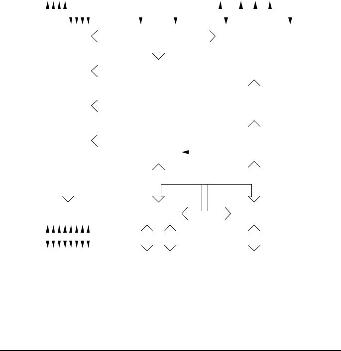
(E43/743/E44 Only)
Figure 1. Functional Block Diagram
2 |
P R E L I M I N A R Y |
CP97DZ83300 |

|
Z86E33/733/E34/E43/743/E44 |
Zilog |
CMOS Z8® OTP Microcontrollers |
|
|
PIN IDENTIFICATION
R//W |
|
1 |
40 |
|
|
/DS |
||
|
|
|||||||
P25 |
|
|
|
|
|
|
|
P24 |
|
|
|
|
|
|
|
||
P26 |
|
|
|
|
|
|
|
P23 |
|
|
|
|
|
|
|
||
P27 |
|
|
|
|
|
|
|
P22 |
|
|
|
|
|
|
|
||
P04 |
|
|
|
|
|
|
|
P21 |
|
|
|
|
|
|
|
||
P05 |
|
|
|
|
|
|
|
P20 |
|
|
|
|
|
|
|
||
P06 |
|
|
|
|
|
|
|
P03 |
|
|
|
|
|
|
|
||
P14 |
|
|
|
|
|
|
|
P13 |
|
|
|
|
|
|
|
||
P15 |
|
|
|
|
|
|
|
P12 |
|
|
|
|
|
|
|
||
P07 |
|
|
|
|
|
|
|
GND |
|
|
|
DIP |
|
|
|
||
|
|
|
|
|
|
|||
VCC |
|
|
|
|
|
|
P02 |
|
|
|
|
|
|
||||
P16 |
|
|
|
|
|
|
|
P11 |
|
|
|
|
|
|
|
||
P17 |
|
|
|
|
|
|
|
P10 |
|
|
|
|
|
|
|
||
XTAL2 |
|
|
|
|
|
|
|
P01 |
|
|
|
|
|
|
|
||
XTAL1 |
|
|
|
|
|
|
|
P00 |
|
|
|
|
|
|
|
||
P31 |
|
|
|
|
|
|
|
P30 |
|
|
|
|
|
|
|
||
P32 |
|
|
|
|
|
|
|
P36 |
|
|
|
|
|
|
|
||
P33 |
|
|
|
|
|
|
|
P37 |
|
|
|
|
|
|
|
||
P34 |
|
|
20 |
21 |
|
|
P35 |
|
|
|
|
|
|||||
/AS |
|
|
|
/RESET |
||||
|
|
|||||||
|
|
|
|
|
|
|
|
|
Figure 2. 40-Pin DIP Pin Configuration
Standard Mode
Table 1. 40-Pin DIP Pin Identification
Standard Mode
Pin # |
Symbol |
Function |
Direction |
|
|
|
|
1 |
R//W |
Read/Write |
Output |
|
|
|
|
2-4 |
P25-P27 |
Port 2, Pins 5,6,7 |
In/Output |
|
|
|
|
5-7 |
P04-P06 |
Port 0, Pins 4,5,6 |
In/Output |
|
|
|
|
8-9 |
P14-P15 |
Port 1, Pins 4,5 |
In/Output |
|
|
|
|
10 |
P07 |
Port 0, Pin 7 |
In/Output |
|
|
|
|
11 |
VCC |
Power Supply |
|
12-13 |
P16-P17 |
Port 1, Pins 6,7 |
In/Output |
|
|
|
|
14 |
XTAL2 |
Crystal Oscillator |
Output |
|
|
|
|
15 |
XTAL1 |
Crystal Oscillator |
Input |
|
|
|
|
16-18 |
P31-P33 |
Port 3, Pins 1,2,3 |
Input |
|
|
|
|
19 |
P34 |
Port 3, Pin 4 |
Output |
|
|
|
|
20 |
/AS |
Address Strobe |
Output |
|
|
|
|
21 |
/RESET |
Reset |
Input |
|
|
|
|
22 |
P35 |
Port 3, Pin 5 |
Output |
|
|
|
|
23 |
P37 |
Port 3, Pin 7 |
Output |
|
|
|
|
24 |
P36 |
Port 3, Pin 6 |
Output |
|
|
|
|
25 |
P30 |
Port 3, Pin 0 |
Input |
|
|
|
|
26-27 |
P00-P01 |
Port 0, Pins 0,1 |
In/Output |
|
|
|
|
28-29 |
P10-P11 |
Port 1, Pins 0,1 |
In/Output |
|
|
|
|
30 |
P02 |
Port 0, Pin 2 |
In/Output |
|
|
|
|
31 |
GND |
Ground |
|
|
|
|
|
32-33 |
P12-P13 |
Port 1, Pins 2,3 |
In/Output |
|
|
|
|
34 |
P03 |
Port 0, Pin 3 |
In/Output |
|
|
|
|
35-39 |
P20-P24 |
Port 2, Pins |
In/Output |
|
|
0,1,2,3,4 |
|
|
|
|
|
40 |
DS |
Data Strobe |
Output |
|
|
|
|
Notes:
Pin Configuration and Identification identical on DIP and Cerdip Window Lid style packages.
CP97DZ83300 |
P R E L I M I N A R Y |
3 |
 Loading...