


 Loading...
ZILOG Z86C8316PEC, Z86C8316PSC, Z86C8316SEC, Z86C8316SSC, Z86C8316VEC Datasheet
...CUSTOMER PROCUREMENT SPECIFICATION
Z86C83/C84 1
Z8® MCU MICROCONTROLLERS
FEATURES
|
ROM |
RAM* |
I/O |
Voltage |
Device |
(KB) |
(Bytes) |
Lines |
Range |
|
|
|
|
|
Z86C83 |
4 |
237 |
21 |
3.0V to 5.5V |
Z86C84 |
4 |
237 |
17 |
3.0V to 5.5V |
|
|
|
|
|
Note: * General-Purpose
■28-Pin DIP, SOIC, and PLCC Packages
■Clock Speed: 16 MHz
■Three Expanded Register Groups
■8-Channel, 8-Bit A/D Converter with Track and Hold, and Unique R-Ladder AGND Offset Control
■Z86C84 has two 8-Bit D/A Converters with Programmable Gain Stages, 3 s Settling Time
■Six Vectored, Prioritized Interrupts from Six Different Sources
■Two Analog Comparator Inputs with Programmable Interrupt Polarity
■Two Programmable 8-Bit Timers, each with a 6-Bit Programmable Prescaler
■Auto Latch Mask Option for P00, P01, and P02
■Power-On Reset (POR) Timer
■Permanent Watch-Dog Timer (WDT) Mask Option
■Software-Programmable Pull-Up Resistors
■On-Chip Oscillator for Crystal, Resonator or LC
GENERAL DESCRIPTION
The Z86C83/C84 Consumer Controller Processors (CCP™ ) are full-featured members of the CMOS Z8 microcontroller family offering a unique register-to-register architecture that avoids accumulator bottlenecks for higher code efficiency than RISC processors.
The Z86C83/C84 are designed to be used in a wide variety of embedded control applications, such as appliances, process controls, keyboards, security systems, battery chargers, and automotive modules.
For applications requiring powerful I/O capabilities, the Z86C83/C84 devices can have up to 21/17 (C83/C84 respectively) pins dedicated to input and output. These lines are grouped into three ports, and are configured by software to provide digital/analog I/O timing and status signals.
An on-chip, half-flash 8-bit ±1/2 Least Significant Bit (LSB) A/D converter can multiplex up to eight analog inputs.
Unused analog inputs revert to standard digital I/O use. Unique, programmable AGND offset control of the A/D resistor ladder compresses the converter's dynamic range for maximum effective 9-bit A/D resolution.
The Z86C84 has two 8-bit ±1/2 LSB D/A converters. High and low reference voltages provide precise control of the output voltage range. Programmable gain for each D/A converter provides a maximum effective 10-bit resolution for many tasks.
On-chip 8-bit counter/timers with many user-selectable modes simplify real-time tasks, such as counting, timing, and generation of PWM signals.
The designer can prioritize six different maskable, vectored, internal or external interrupts for efficient interrupt handling and multitasking functions.
DS96DZ80203 |
1 |

Z86C83/C84
Z8® MCU Microcontrollers
GENERAL DESCRIPTION (Continued)
By means of an expanded register file, the designer has access to additional control registers for configuring peripheral functions including the A/D and D/A converters, counter/timers, and I/O port functions (Figure 1).
Notes: All Signals with a preceding front slash, "/", are active Low, e.g., B//W (WORD is active Low); /B/W (BYTE is active Low, only).
Power connections follow conventional descriptions below:
Connection |
Circuit |
Device |
|
|
|
Power |
VCC |
VCC |
Ground |
GND |
VSS |
P00 |
|
Comparators |
|
Register File |
|
|
|
(2) |
|
256 x 8-Bit |
|
|
|
P01 |
|
|
|
P31 |
||
|
|
|
|
|
||
P02 |
|
|
|
|
|
P32 |
P03† |
Port 0 |
|
|
|
Port 3 |
P33 |
|
|
|
|
|
||
P04† |
|
Register Bus |
|
|
P34 |
|
|
|
|
|
|
||
P05† |
|
|
|
Internal |
|
P35 |
P06† |
|
|
Address Bus |
|
P36 |
|
|
|
|
|
|
|
|
VDHI ** |
|
ROM |
|
Z8® Core |
|
|
**Dual |
4K x 8 |
|
|
|
||
VDL0 ** |
|
|
|
|
||
DAC1 ** |
8-Bit |
|
Internal Data Bus |
|
XTAL 1/2 |
|
DAC |
|
Machine |
||||
DAC2 ** |
|
|
|
|
||
|
|
|
|
Timing |
|
|
|
|
|
|
|
|
|
AC0/P20 |
|
|
|
|
and |
/RESET |
AC1/P21 |
|
|
|
|
Instruction |
|
|
|
|
|
|
||
AC2/P22 |
|
|
|
Expanded |
Control |
|
AC3/P23 |
|
|
Expanded |
Register Bus |
|
|
Port 2 |
|
|
|
|
||
AC4/P24 |
Register File |
|
|
|||
AC5/P25 |
|
|
|
|
|
VCC |
AC6/P26 |
|
|
|
|
Power |
|
|
|
|
|
GND |
||
AC7/P27 |
|
|
|
|
|
|
AVCC |
8-Channel |
|
|
Counter/Timer |
Notes: |
|
|
|
** Not available on Z86C83. |
||||
|
8-Bit A/D |
|
|
8-Bit (2) |
||
AGND |
|
|
† Not available on Z86C84. |
|||
|
|
|
|
|||
Figure 1. Z86C83/C84 Functional Block Diagram
2 |
DS96DZ80203 |

Z86C83/C84
Z8® MCU Microcontrollers
PIN DESCRIPTION
Table 1. Z86C83 28-Pin DIP, SOIC Pin Identification*
No |
Symbol |
Function |
Direction |
|
|
|
|
1-7 |
P21-P27 |
Port 2, Bit 1-7 |
Input/Output |
|
or AC1-AC7 |
Analog In 1-7 |
|
8 |
/RESET |
Reset |
Input |
9 |
XTAL1 |
Oscillator Clock |
Input |
10 |
XTAL2 |
Oscillator Clock |
Output |
11 |
GND |
Ground |
|
12 |
VCC |
Power |
|
13-15 |
P31-P33 |
Port 3, Bits 1-3 |
Input |
16 |
P34 |
Port 3, Bit 4 |
Output |
17 |
P36 |
Port 3, Bit 6 |
Output |
18 |
P35 |
Port 3, Bit 5 |
Output |
19-25 |
P0-P06 |
Port 0, Bits 0-6 |
Input/Output |
26 |
AGND |
Analog Ground |
|
27 |
AVCC |
Analog Power |
|
28 |
P20 |
Port 2, Bit 0 |
Input/Output |
|
or AC0 |
Analog In 0 |
|
|
|
|
|
Note:
* DIP and SOIC Pin Description and Configuration are identical.
P21/AC1 |
|
|
|
1 |
|
28 |
|
P20/AC0 |
|
|
|
|
|||||
|
|
|
||||||
P22/AC2 |
|
2 |
|
27 |
|
AVCC |
||
|
|
|
|
|||||
P23/AC3 |
|
|
|
3 |
|
26 |
|
AGND |
|
|
|
|
|||||
P24/AC4 |
|
|
|
4 |
|
25 |
|
P06 |
|
|
|
|
|||||
|
|
|
||||||
P25/AC5 |
|
5 |
|
24 |
|
P05 |
||
|
|
|
|
|||||
|
|
|
||||||
P26/AC6 |
|
|
6 |
|
23 |
|
P04 |
|
|
|
|
||||||
|
|
|
7 |
Z86C83 |
22 |
|
||
P27/AC7 |
|
|
P03 |
|||||
|
|
|
||||||
|
|
|
8 |
21 |
|
|||
/RESET |
|
|
|
|
P02 |
|||
|
|
|
||||||
|
|
|
9 |
|
|
|||
XTAL1 |
|
|
|
20 |
|
P01 |
||
|
|
|
|
|||||
|
|
|
10 |
|
19 |
|
||
XTAL2 |
|
|
|
|
P00 |
|||
|
|
|
|
|
||||
|
|
|
11 |
|
18 |
|
||
GND |
|
|
|
|
|
P35 |
||
|
|
|
|
|
||||
VCC |
|
|
|
12 |
|
17 |
|
P36 |
|
|
|
|
|||||
P31 |
|
|
|
13 |
|
16 |
|
P34 |
|
|
|
|
|
||||
P32 |
|
|
|
14 |
|
15 |
|
P33 |
|
|
|
|
|
||||
|
|
|
|
|
||||
|
|
|
|
|
|
|
|
|
Standard Mode
Table 2. Z86C84 28-Pin DIP, SOIC Pin Identification*
No |
Symbol |
Function |
Direction |
|
|
|
|
1-7 |
P21-P27 |
Port 2, Bit 1-7 |
Input/Output |
|
or AC1-AC7 |
Analog In 1-7 |
|
8 |
/RESET |
Reset |
Input |
9 |
XTAL1 |
Oscillator Clock |
Input |
10 |
XTAL2 |
Oscillator Clock |
Output |
11 |
GND |
Ground |
|
12 |
VCC |
Power |
|
13-15 P31-P33 |
Port 3, Bits 1-3 |
Input |
|
16 |
P34 |
Port 3, Bit 4 |
Output |
17 |
P36 |
Port 3, Bit 6 |
Output |
18 |
P35 |
Port 3, Bit 5 |
Output |
19-21 P0-P02 |
Port 0, Bits 0-3 |
Input/Output |
|
22 |
VDLO |
D/A Ref. Volt.,Low |
Input |
23 |
VDHI |
D/A Ref. Volt.,High |
Input |
24-25 DAC2-1 |
D/A Converter |
Output |
|
26 |
AGND |
Analog Ground |
|
27 |
AVCC |
Analog Power |
|
28 |
P20 |
Port 2, Bit 0 |
Input/Output |
|
or AC0 |
Analog In 0 |
|
|
|
|
|
Note:
* DIP and SOIC Pin Description and Configuration are identical
P21/AC1 |
|
|
|
1 |
|
28 |
|
P20/AC0 |
|
|
|
|
|||||
|
|
|
||||||
P22/AC2 |
|
2 |
|
27 |
|
AVCC |
||
|
|
|
|
|||||
P23/AC3 |
|
|
|
3 |
|
26 |
|
AGND |
|
|
|
|
|||||
P24/AC4 |
|
|
|
4 |
|
25 |
|
DAC1 |
|
|
|
|
|||||
|
|
|
||||||
P25/AC5 |
|
5 |
|
24 |
|
DAC2 |
||
|
|
|
|
|||||
|
|
|
||||||
P26/AC6 |
|
|
6 |
|
23 |
|
VDHI |
|
|
|
|
||||||
|
|
|
7 |
Z86C84 |
22 |
|
||
P27/AC7 |
|
|
VDLO |
|||||
|
|
|
||||||
|
|
|
8 |
21 |
|
|||
/RESET |
|
|
|
|
P02 |
|||
|
|
|
||||||
|
|
|
9 |
|
|
|||
XTAL1 |
|
|
|
20 |
|
P01 |
||
|
|
|
|
|||||
|
|
|
10 |
|
19 |
|
||
XTAL2 |
|
|
|
|
P00 |
|||
|
|
|
|
|
||||
|
|
|
11 |
|
18 |
|
||
GND |
|
|
|
|
|
P35 |
||
|
|
|
|
|
||||
|
|
|
12 |
|
17 |
|
||
VCC |
|
|
|
|
|
P36 |
||
|
|
|
|
|||||
P31 |
|
|
|
13 |
|
16 |
|
P34 |
|
|
|
|
|
||||
|
|
|
14 |
|
15 |
|
||
P32 |
|
|
|
|
|
P33 |
||
|
|
|
|
|
||||
|
|
|
|
|
||||
|
|
|
|
|
|
|
|
|
* Standard Mode
Figure 2. Z86C83 28-Pin DIP and SOIC Pin
Configuration* Figure 3. Z86C84 28-Pin DIP and SOIC Pin Configuration*
DS96DZ80203 |
3 |

Z86C83/C84
Z8® MCU Microcontrollers
PIN DESCRIPTION (Continued)
Table 3. Z86C83 28-Pin PLCC Pin Identification
No |
Symbol |
Function |
Direction |
1-8 |
P20-P27 |
Port 2, Bit 0-7 |
Input/Output |
|
or AC0-AC7 |
Analog In 0-7 |
|
9 |
/RESET |
Reset |
Input |
10 |
XTAL1 |
Oscillator Clock |
Input |
11 |
XTAL2 |
Oscillator Clock |
Output |
12 |
GND |
Ground |
|
13 |
VCC |
Power |
|
14-16 P31-P33 |
Port 3, Bits 1-3 |
Input |
|
17 |
P34 |
Port 3, Bit 4 |
Output |
18 |
P36 |
Port 3, Bit 6 |
Output |
19 |
P35 |
Port 3, Bit 5 |
Output |
20-26 P00-P06 |
Port 0, Bits 0-6 |
Input/Output |
|
27 |
AGND |
Analog Ground |
|
28 |
AVCC |
Analog Power |
|
|
|
|
|
|
|
|
|
|
P23/AC3 |
|
P22/AC2 |
|
P21/AC1 |
|
P20/AC0 |
|
AVCC |
|
AGND |
|
P06 |
|
|
||
|
|
|
|
|
|
|
|
|
|
|
|
|
|
|
|
|
|
|
|
|
|
|
|
|
|
|
|
|
|
|
|
|
|
|
|
|
|
|
|
|
|
|
|
P24/AC4 |
|
4 |
3 |
2 |
1 |
28 |
27 |
26 |
|
|
|
|
|||||||||
|
5 |
|
|
|
|
|
|
|
|
|
|
|
|
|
|
|
25 |
|
P05 |
||
|
|
|
|
|
|
|
|
|
|
|
|
|
|
|
|
||||||
P25/AC5 |
|
6 |
|
|
|
|
|
|
|
|
|
|
|
|
|
|
|
24 |
|
P04 |
|
|
|
|
|
|
|
|
|
|
|
|
|
|
|
|
|
||||||
P26/AC6 |
|
7 |
|
|
|
|
|
|
|
Z86C83 |
|
|
|
|
23 |
|
P03 |
||||
|
|
|
|
|
|
|
|
|
|
|
|
||||||||||
P27/AC7 |
|
8 |
|
|
|
|
|
|
|
|
|
|
|
22 |
|
P02 |
|||||
|
|
|
|
|
|
|
|
|
|
|
|
|
|||||||||
|
|
|
|
|
|
|
|
PLCC |
|
|
|
|
|||||||||
/RESET |
|
9 |
|
|
|
|
|
|
|
|
|
|
|
21 |
|
P01 |
|||||
|
|
|
|
|
|
|
|
|
|
|
|
|
|
|
|
||||||
XTAL1 |
|
10 |
|
|
|
|
|
|
|
|
|
|
|
|
|
|
20 |
|
P00 |
||
|
|
|
|
|
|
|
|
|
|
|
|
|
|
|
|
||||||
XTAL2 |
|
11 |
|
|
|
|
|
|
|
|
|
|
|
|
|
|
|
19 |
|
P35 |
|
|
|
|
|
|
|
|
|
|
|
|
|
|
|
|
|
||||||
|
|
|
|
|
|
|
|
|
|
|
|
|
|
||||||||
|
12 |
13 |
14 |
15 |
16 |
17 |
18 |
|
|
|
|
||||||||||
|
|
|
|
|
|
|
|
|
|
|
|
|
|
|
|
|
|
|
|
|
|
|
|
|
|
|
|
|
|
|
|
|
|
|
|
|
|
|
|
|
|
|
|
|
|
|
|
|
GND |
|
VCC |
|
P31 |
|
P32 |
|
P33 |
|
P34 |
|
P36 |
|
|
||
Figure 4. Z86C83 28-Pin PLCC Pin Configuration
Table 4. Z86C84 28-Pin PLCC Pin Identification
No |
Symbol |
Function |
Direction |
1-8 |
P20-P27 |
Port 2, Bit 0-7 |
Input/Output |
|
or AC0-AC7 |
Analog In 0-7 |
|
9 |
/RESET |
Reset |
Input |
10 |
XTAL1 |
Oscillator Clock |
Input |
11 |
XTAL2 |
Oscillator Clock |
Output |
12 |
GND |
Ground |
|
13 |
VCC |
Power |
|
14-16 P31-P33 |
Port 3, Bits 1-3 |
Input |
|
17 |
P34 |
Port 3, Bit 4 |
Output |
18 |
P36 |
Port 3, Bit 6 |
Output |
19 |
P35 |
Port 3, Bit 5 |
Output |
20-22 P00-P02 |
Port 0, Bits 0-3 |
Input/Output |
|
23 |
VDLO |
D/A Ref. Volt,Low |
Input |
24 |
VDHI |
D/A Ref. Volt.,High |
Input/Output |
25-26 DAC2-DAC1 |
D/A Converter |
Output |
|
27 |
AGND |
Analog Ground |
|
28 |
AVCC |
Analog Power |
|
|
|
|
|
|
|
|
|
|
P23/AC3 |
|
P22/AC2 |
|
P21/AC1 |
|
P20/AC0 |
|
AVCC |
|
AGND |
|
DAC1 |
|
|
||
|
|
|
|
|
|
|
|
|
|
|
|
|
|
|
|
|
|
|
|
|
|
|
|
|
|
|
|
|
|
|
|
|
|
|
|
|
|
|
|
|
|
|
|
P24/AC4 |
|
4 |
3 |
2 |
1 |
28 |
27 |
26 |
|
|
|
|
|||||||||
|
5 |
|
|
|
|
|
|
|
|
|
|
|
|
|
|
|
25 |
|
DAC2 |
||
|
|
|
|
|
|
|
|
|
|
|
|
|
|
|
|
||||||
P25/AC5 |
|
6 |
|
|
|
|
|
|
|
|
|
|
|
|
|
|
|
24 |
|
VDHI |
|
|
|
|
|
|
|
|
|
|
|
|
|
|
|
|
|
||||||
P26/AC6 |
|
7 |
|
|
|
|
|
|
|
Z86C84 |
|
|
|
|
23 |
|
VDLO |
||||
|
|
|
|
|
|
|
|
|
|
|
|
||||||||||
P27/AC7 |
|
8 |
|
|
|
|
|
|
|
|
|
|
|
22 |
|
P02 |
|||||
|
|
|
|
|
|
|
|
|
|
|
|
|
|||||||||
|
|
|
|
|
|
|
|
PLCC |
|
|
|
|
|||||||||
/RESET |
|
9 |
|
|
|
|
|
|
|
|
|
|
|
21 |
|
P01 |
|||||
|
|
|
|
|
|
|
|
|
|
|
|
|
|
|
|
||||||
XTAL1 |
|
10 |
|
|
|
|
|
|
|
|
|
|
|
|
|
|
20 |
|
P00 |
||
|
|
|
|
|
|
|
|
|
|
|
|
|
|
|
|
||||||
XTAL2 |
|
11 |
|
|
|
|
|
|
|
|
|
|
|
|
|
|
|
19 |
|
P35 |
|
|
|
|
|
|
|
|
|
|
|
|
|
|
|
|
|
||||||
|
|
|
|
|
|
|
|
|
|
|
|
|
|
||||||||
|
12 |
13 |
14 |
15 |
16 |
17 |
18 |
|
|
|
|
||||||||||
|
|
|
|
|
|
|
|
|
|
|
|
|
|
|
|
|
|
|
|
|
|
|
|
|
|
|
|
|
|
|
|
|
|
|
|
|
|
|
|
|
|
|
|
|
|
|
|
|
GND |
|
VCC |
|
P31 |
|
P32 |
|
P33 |
|
P34 |
|
P36 |
|
|
||
Figure 5. Z86C84 28-Pin PLCC Pin Configuration
4 |
DS96DZ80203 |
Z86C83/C84
Z8® MCU Microcontrollers
ABSOLUTE MAXIMUM RATINGS
Parameter |
Min |
Max |
Units |
|
|
|
|
Ambient Temperature under Bias |
–40 |
+105 |
C |
Storage Temperature |
–65 |
+150 |
C |
Voltage on any Pin with Respect to VSS [Note 1] |
–0.6 |
+7 |
V |
Voltage on VCC Pin with Respect to VSS |
–0.3 |
+7 |
V |
Voltage on /RESET Pins with Respect to VSS [Note 2] |
–0.6 |
VCC+1 |
V |
Total Power Dissipation |
|
770 |
mW |
Maximum Current out of VSS |
|
140 |
mA |
Maximum Current into VCC |
|
125 |
mA |
Maximum Current into an Input Pin [Note 3] |
–600 |
+600 |
A |
Maximum Current into an Open-Drain Pin [Note 4] |
–600 |
+600 |
A |
Maximum Output Current Sinked by Any I/O Pin |
|
25 |
mA |
Maximum Output Current Sourced by Any I/O Pin |
|
25 |
mA |
|
|
|
|
Notes:
1.This applies to all pins except XTAL and /RESET pins and where otherwise noted.
2.There is no input protection diode from pin to VCC.
3.This excludes XTAL pins.
4.Device pin is not at an output Low state.
Notice:
Stresses greater than those listed under Absolute Maximum Ratings may cause permanent damage to the device. This is a stress rating only; functional operation of the device at any condition above those indicated in the operational sections of these specifications is not implied. Exposure to absolute maximum rating conditions for an extended period may affect device reliability.
Total power dissipation should not exceed 770 mW for the |
|
package. Power dissipation is calculated as follows: |
|
Total Power Dissipation = |
VCC x [ ICC – (sum of IOH) ] |
+ sum of [ (VCC – VOH) x IOH ] + sum of (V0L x I0L)
STANDARD TEST CONDITIONS
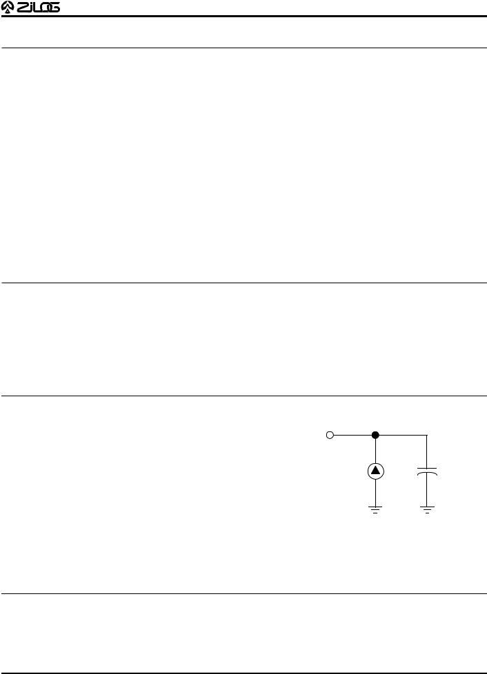
The characteristics listed below apply for standard test conditions as noted. All voltages are referenced to Ground. Positive current flows into the referenced pin (Figure 6).
From Output
Under Test
I |
150 pF |
Figure 6. Test Load Diagram
VDD SPECIFICATION
VDD = 3.0V to 5.5V
DS96DZ80203 |
5 |

Z86C83/C84
Z8® MCU Microcontrollers
CAPACITANCE
TA = 25°C, VCC = GND = 0V, f = 1.0 MHz, unmeasured pins returned to GND.
Parameter |
Min |
Max |
|
|
|
Input capacitance |
0 |
20 pF |
Output capacitance |
0 |
20pF |
I/O capacitance |
0 |
20 pF |
|
|
|
6 |
DS96DZ80203 |

Z86C83/C84
Z8® MCU Microcontrollers
DC ELECTRICAL CHARACTERISTICS
|
|
VCC |
TA = 0° C |
TA = –40°C |
Typical |
|
|
|
||
|
|
to +70°C |
to +105°C |
[13] |
|
|
|
|||
Sym |
Parameter |
Note 3 |
Min |
Max |
Min |
Max |
@ 25°C Units Conditions |
Notes |
||
|
|
|
|
|
|
|
|
|
|
|
VCH |
Clock Input High |
3.0V |
0.7 VCC |
VCC+0.3 |
0.7 VCC |
VCC+0.3 |
1.3 |
V |
Driven by External Clock |
|
|
Voltage |
|
|
|
|
|
|
|
Generator |
|
|
|
5.5V |
0.7 VCC |
VCC+0.3 |
0.7 VCC |
VCC+0.3 |
2.5 |
V |
Driven by External Clock |
|
|
|
|
|
|
|
|
|
|
Generator |
|
VCL |
Clock Input Low |
3.0V |
GND-0.3 |
0.2 VCC |
GND-0.3 |
0.2 VCC |
0.7 |
V |
Driven by External Clock |
|
|
Voltage |
|
|
|
|
|
|
|
Generator |
|
|
|
5.5V |
GND-0.3 |
0.2 VCC |
GND-0.3 |
0.2 VCC |
1.5 |
V |
Driven by External Clock |
|
|
|
|
|
|
|
|
|
|
Generator |
|
VIH |
Input High Voltage |
3.0V |
0.7 VCC |
VCC+0.3 |
0.7 VCC |
VCC+0.3 |
1.3 |
V |
|
|
|
|
5.5V |
0.7 VCC |
VCC+0.3 |
0.7 VCC |
VCC+0.3 |
2.5 |
V |
|
|
|
|
|
|
|
|
|
|
|
|
|
VIL |
Input Low Voltage |
3.0V |
GND-0.3 |
0.2 VCC |
GND-0.3 |
0.2 VCC |
0.7 |
V |
|
|
|
|
5.5V |
GND-0.3 |
0.2 VCC |
GND-0.3 |
0.2 VCC |
1.5 |
V |
|
|
|
|
|
|
|
|
|
|
|
|
|
VOH1 |
Output High |
3.0V |
VCC-0.4 |
|
VCC-0.4 |
|
3.1 |
V |
IOH = -2.0 mA |
8 |
|
Voltage |
|
|
|
|
|
|
|
|
|
|
5.5V |
VCC-0.4 |
|
VCC-0.4 |
|
4.8 |
V |
IOH = -2.0 mA |
8 |
|
|
|
|
|
|||||||
|
|
|
|
|
|
|
|
|
|
|
VOL1 |
Output Low |
3.0V |
|
0.6 |
|
0.6 |
0.2 |
V |
IOL = +4.0 mA |
8 |
|
Voltage |
|
|
|
|
|
|
|
|
|
|
5.5V |
|
0.4 |
|
0.4 |
0.1 |
V |
IOL = +4.0 mA |
8 |
|
|
|
|
|
|||||||
|
|
|
|
|
|
|
|
|
|
|
VOL2 |
Output Low |
3.0V |
|
1.2 |
|
1.2 |
0.3 |
V |
IOL = +6 mA |
8 |
|
Voltage |
|
|
|
|
|
|
|
|
|
|
5.5V |
|
1.2 |
|
1.2 |
0.3 |
V |
IOL = +12 mA |
8 |
|
|
|
|
|
|||||||
VRH |
Reset Input High |
3.0V |
.8 VCC |
VCC |
.8 VCC |
VCC |
1.5 |
V |
|
|
|
Voltage |
|
|
|
|
|
|
|
|
|
|
5.5V |
.8 VCC |
VCC |
.8 VCC |
VCC |
2.1 |
V |
|
|
|
|
|
|
|
|||||||
VRl |
Reset Input Low |
3.0V |
GND-0.3 |
0.2 VCC |
GND-0.3 |
0.2 VCC |
1.1 |
V |
|
|
|
Voltage |
|
|
|
|
|
|
|
|
|
|
5.5V |
GND-0.3 |
0.2 VCC |
GND-0.3 |
0.2 VCC |
1.7 |
V |
|
|
|
|
|
|
|
|||||||
|
|
|
|
|
|
|
|
|
|
|
VOFFSET |
Comparator Input |
3.0V |
|
25 |
|
25 |
10 |
mV |
|
10 |
|
Offset |
|
|
|
|
|
|
|
|
|
|
|
|
|
|
|
|
|
|
|
|
|
Voltage |
5.5V |
|
25 |
|
25 |
10 |
mV |
|
10 |
|
|
|
|
|
|
|
|
|
|
|
IIL |
Input Leakage |
3.0V |
-1 |
1 |
-1 |
2 |
<1 |
A |
VIN = OV, VCC |
|
|
|
5.5V |
-1 |
1 |
-1 |
2 |
<1 |
A |
VIN = OV, VCC |
|
|
|
|
|
|
|
|
|
|
|
|
IOL |
Output Leakage |
3.0V |
-1 |
1 |
-1 |
2 |
<1 |
A |
VIN = OV, VCC |
|
|
|
5.5V |
-1 |
1 |
-1 |
2 |
<1 |
A |
VIN = OV, VCC |
|
IIR |
Reset Input |
3.0V |
|
-130 |
|
-130 |
-25 |
A |
|
|
|
Current |
5.5V |
|
-180 |
|
-180 |
-40 |
A |
|
|
|
|
|
|
|
|
|
|
|
|
|
ICC |
Supply Current |
3.0V |
|
20 |
|
20 |
7 |
mA |
@ 16 MHz |
4, 15 |
|
|
5.5V |
|
25 |
|
25 |
20 |
mA |
@ 16 MHz |
4, 15 |
|
|
|
|
|
|
|
|
|
|
|
|
|
5.0V |
|
7 |
|
7 |
3 |
mA |
@ 3.58 MHz |
4, 15 |
|
|
|
|
|
|
|
|
|
|
|
|
|
5.0V |
|
10 |
|
10 |
5 |
mA |
@ 8 MHz |
4, 15 |
|
|
|
|
|
|
|
|
|
|
|
ICC1 |
Standby Current |
3.0V |
|
4.5 |
|
4.5 |
2.0 |
mA |
HALT Mode VIN = OV, VCC @ 16 |
4 |
|
|
|
|
|
|
|
|
|
MHz |
|
|
|
|
|
|
|
|
|
|
|
|
|
|
5.5V |
|
8 |
|
8 |
3.7 |
mA |
HALT Mode VIN = OV, VCC @ 16 |
4 |
|
|
|
|
|
|
|
|
|
MHz |
|
|
|
|
|
|
|
|
|
|
|
|
|
|
3.0V |
|
3.4 |
|
3.4 |
1.5 |
mA |
Clock Divide-by-16 @ 16 MHz |
4 |
|
|
|
|
|
|
|
|
|
|
|
|
|
5.5V |
|
7.0 |
|
7.0 |
2.9 |
mA |
Clock Divide-by-16 @ 16 MHz |
4 |
|
|
|
|
|
|
|
|
|
|
|
DS96DZ80203 |
7 |

Z86C83/C84 |
|
|
|
|
|
|
|
|
|
|
||
Z8® |
MCU Microcontrollers |
|
|
|
|
|
|
|
|
|
||
|
|
|
|
|
|
|
|
|
|
|
||
|
|
|
|
|
|
|
|
|
|
|
||
|
|
|
VCC |
TA = 0° C |
|
TA = –40°C |
Typical |
|
|
|
||
|
|
|
to +70°C |
|
to +105°C |
[13] |
|
|
|
|||
Sym Parameter |
Note 3 |
Min |
Max |
|
Min |
Max |
@ 25°C Units Conditions |
Notes |
||||
|
|
|
|
|
|
|
|
|
|
|
|
|
ICC2 |
|
Standby Current |
3.0V |
|
8 |
|
|
15 |
1 |
A STOP Mode VIN = OV, |
6,11,15 |
|
|
|
|
|
|
|
|
|
|
|
|
VCC WDT is not Running |
|
|
|
|
5.5V |
|
10 |
|
|
20 |
2 |
A |
STOP Mode VIN = OV, |
6,11,15 |
|
|
|
|
|
|
|
|
|
|
|
VCC WDT is not Running |
|
|
|
|
3.0V |
|
500 |
|
|
600 |
310 |
A |
STOP Mode VIN = OV, |
6,11,14, |
|
|
|
|
|
|
|
|
|
|
|
VCC WDT is Running |
15 |
|
|
|
5.5V |
|
800 |
|
|
1000 |
600 |
A |
STOP Mode VIN = OV, |
6,11,14, |
|
|
|
|
|
|
|
|
|
|
|
VCC WDT is Running |
15 |
VICR |
|
Input Common |
3.0 |
0 |
VCC-1.0V |
0 |
VCC-1.5V |
|
V |
|
10 |
|
|
|
Mode |
|
|
|
|
|
|
|
|
|
|
|
|
Voltage Range |
5.5 |
0 |
VCC-1.0V |
0 |
VCC-1.5V |
|
V |
|
10 |
|
|
|
|
|
|
|
|
|
|
|
|
|
|
IALL |
|
Auto Latch Low |
3.0V |
|
8 |
|
|
10 |
5 |
A |
OV < VIN < VCC |
9 |
|
|
Current |
|
|
|
|
|
|
|
|
|
|
|
|
5.5V |
|
15 |
|
|
20 |
11 |
A |
OV < VIN < VCC |
9 |
|
|
|
|
|
|
|
|
|
|
|
|
|
|
IALH |
|
Auto Latch High |
3.0V |
|
-5 |
|
|
-7 |
-3 |
A |
OV < VIN < VCC |
9 |
|
|
Current |
|
|
|
|
|
|
|
|
|
|
|
|
5.5V |
|
-8 |
|
|
-10 |
-6 |
A |
OV < VIN < VCC |
9 |
|
VLV |
|
VCC Low-Voltage |
|
2.0 |
3.3 |
|
2.2 |
3.6 |
3.0 |
V |
2 MHz max Int. CLK Freq. |
7 |
|
|
Protection Voltage |
|
|
|
|
|
|
|
|
|
|
|
|
|
|
|
|
|
|
|
|
|
||
Notes: |
|
|
|
|
|
|
|
|
|
|
||
1. |
ICC1 |
Typical |
Max |
Unit |
|
Freq |
|
|
|
|
||
|
Clock-Driven |
0.3 mA |
5 |
|
mA |
|
8 MHz |
|
|
|
|
|
2.GND = 0V.
3.3.0V VCC voltage specification guarantees 3.3V ±0.3V, and 5.5V VCC voltage specification guarantees 5.0V ±0.5V.
4.All outputs unloaded, I/O pins floating, inputs at rail.
5.CL1 = CL2 = 100 pF.
6.Same as note [4] except inputs at VCC.
7.The VLV increases as the temperature decreases.
8.Standard Mode (not Low EMI).
9.Auto Latch (mask option) selected.
10.For analog comparator, inputs when analog comparators are enabled.
11.Clock must be forced Low, when XTAL 1 is clock-driven and XTAL2 is floating.
12.Excludes clock pins.
13.Typicals are at VCC = 5.0V and 3.3V.
14.Internal RC selected.
15.Combined Digital and Analog VCC supply current.
8 |
DS96DZ80203 |
Z86C83/C84
Z8® MCU Microcontrollers
AC ELECTRICAL CHARACTERISTICS
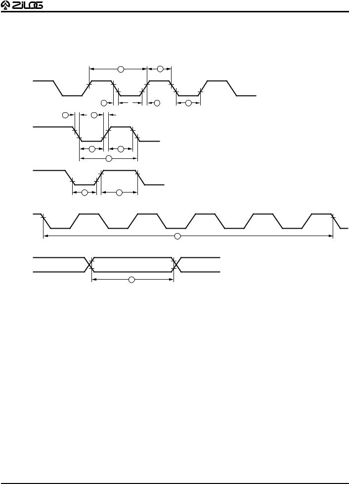
Additional Timing Diagram
1 |
3 |
Clock
2 |
2 |
3 |
7 |
7 |
TIN |
|
4 |
5 |
|
6 |
IRQN |
|
8 |
9 |
Clock
Setup
11
Stop-Mode
Recovery
Source
10
Figure 7. Additional Timing
DS96DZ80203 |
9 |

Z86C83/C84
Z8® MCU Microcontrollers
AC ELECTRICAL CHARACTERISTICS (Continued)
Additional Timing Table (SCLK/TCLK = XTAL/2)
|
|
|
VCC |
TA = 0°C to +70°C |
|
TA = –40°C to +105°C |
|
|
|
|||||
No Symbol |
Parameter |
12 MHz |
16 MHz |
12 MHz |
16 MHz |
|
|
|
||||||
Note 6 |
Min |
Max |
Min |
Max |
Min |
Max |
Min |
Max |
Units |
Notes |
||||
|
|
|
|
|
|
|
|
|
|
|
|
|
|
|
1 |
TpC |
Input Clock Period |
3.0V |
83 |
DC |
62.5 |
DC |
83 |
DC |
62.5 |
DC |
ns |
|
1 |
|
|
|
5.5V |
83 |
DC |
62.5 |
DC |
83 |
DC |
62.5 |
DC |
ns |
|
1 |
|
|
|
|
|
|
|
|
|
|
|
|
|
|
|
2 |
TrC,TfC |
Clock Input Rise & Fall |
3.0V |
|
15 |
|
15 |
|
15 |
|
15 |
ns |
|
1 |
|
|
Times |
5.5V |
|
15 |
|
15 |
|
15 |
|
15 |
ns |
|
1 |
|
|
|
|
|
|
|
|
|
|
|
|
|
|
|
3 |
TwC |
Input Clock Width |
3.0V |
41 |
|
31 |
|
41 |
|
31 |
|
ns |
|
1 |
|
|
|
5.5V |
41 |
|
31 |
|
41 |
|
31 |
|
ns |
|
1 |
|
|
|
|
|
|
|
|
|
|
|
|
|
|
|
4 |
TwTinL |
Timer Input Low Width |
3.0V |
100 |
|
100 |
|
100 |
|
100 |
|
ns |
|
1 |
|
|
|
5.5V |
70 |
|
70 |
|
70 |
|
70 |
|
ns |
|
1 |
|
|
|
|
|
|
|
|
|
|
|
|
|
|
|
5 |
TwTinH |
Timer Input High Width |
3.0V |
5TpC |
|
5TpC |
|
5TpC |
|
5TpC |
|
|
|
1 |
|
|
|
5.5V |
5TpC |
|
5TpC |
|
5TpC |
|
5TpC |
|
|
|
1 |
|
|
|
|
|
|
|
|
|
|
|
|
|
|
|
6 |
TpTin |
Timer Input Period |
3.0V |
8TpC |
|
8TpC |
|
8TpC |
|
8TpC |
|
|
|
1 |
|
|
|
5.5V |
8TpC |
|
8TpC |
|
8TpC |
|
8TpC |
|
|
|
1 |
|
|
|
|
|
|
|
|
|
|
|
|
|
|
|
7 |
TrTin, |
Timer Input Rise & Fall |
3.0V |
|
100 |
|
100 |
|
100 |
|
100 |
ns |
|
1 |
|
|
Timer |
|
|
|
|
|
|
|
|
|
|
|
|
|
TfTin |
|
|
|
|
|
|
|
|
|
|
|
|
|
|
|
5.5V |
|
100 |
|
100 |
|
100 |
|
100 |
ns |
|
1 |
|
|
|
|
|
|
|
|
|
|
|
|
|
|
|
|
8A |
TwIL |
Int. Request Low Time |
3.0V |
100 |
|
100 |
|
100 |
|
100 |
|
ns |
1,2 |
|
|
|
|
5.5V |
70 |
|
70 |
|
70 |
|
70 |
|
ns |
1,2 |
|
|
|
|
|
|
|
|
|
|
|
|
|
|
|
|
8B |
TwIL |
Int. Request Low Time |
3.0V |
5TpC |
|
5TpC |
|
5TpC |
|
5TpC |
|
|
1,3 |
|
|
|
|
5.5V |
5TpC |
|
5TpC |
|
5TpC |
|
5TpC |
|
|
1,3 |
|
|
|
|
|
|
|
|
|
|
|
|
|
|
|
|
9 |
TwIH |
Int. Request Input High |
3.0V |
5TpC |
|
5TpC |
|
5TpC |
|
5TpC |
|
|
1,2 |
|
|
|
Time |
5.5V |
5TpC |
|
5TpC |
|
5TpC |
|
5TpC |
|
|
1,2 |
|
|
|
|
|
|
|
|
|
|
|
|
|
|
|
|
10 |
Twsm |
STOP-Mode Recovery |
3.0V |
12 |
|
12 |
|
12 |
|
12 |
|
ns |
|
|
|
|
Width Spec |
5.5V |
12 |
|
12 |
|
12 |
|
12 |
|
ns |
|
|
|
|
|
|
|
|
|
|
|
|
|
|
|
|
|
11 |
Tost |
Oscillator Startup Time |
3.0V |
|
5TpC |
|
5TpC |
|
5TpC |
|
5TpC |
|
|
4 |
|
|
|
5.5V |
|
5TpC |
|
5TpC |
|
5TpC |
|
5TpC |
|
|
4 |
|
|
|
|
|
|
|
|
|
|
|
|
|
|
|
12 |
Twdt |
Watch-Dog Timer Delay |
|
|
|
|
|
|
|
|
WDTMR |
Reg. |
D1 |
D0 |
|
|
Time |
|
|
|
|
|
|
|
|
|
|
|
|
|
|
3.0V |
6.25 |
|
6.25 |
|
6.25 |
|
6.25 |
|
ms |
0 |
0 |
|
|
|
|
|
|
|
|
|
|
|
|
|
|
|
|
|
|
|
3.0V |
12.5 |
|
12.5 |
|
12.5 |
|
12.5 |
|
ms |
0 |
1 |
|
|
|
|
|
|
|
|
|
|
|
|
|
|
|
|
|
|
3.0V |
25 |
|
25 |
|
25 |
|
25 |
|
ms |
1 |
0 |
|
|
|
|
|
|
|
|
|
|
|
|
|
|
|
|
|
|
3.0V |
100 |
|
100 |
|
100 |
|
100 |
|
ms |
1 |
1 |
|
|
|
|
|
|
|
|
|
|
|
|
|
|
|
13 |
TPOR |
Power On Reset Delay |
3.0V |
7 |
24 |
7 |
25 |
7 |
24 |
7 |
25 |
ms |
|
|
|
|
|
5.5V |
3 |
13 |
3 |
14 |
3 |
13 |
3 |
14 |
ms |
|
|
|
|
|
|
|
|
|
|
|
|
|
|
|
|
|
Notes:
1.Timing Reference uses 0.7 VCC for a logic 1 and 0.2 VCC for a logic 0.
2.Interrupt request via Port 3 (P31-P33).
3.Interrupt request via Port 3 (P30).
4.SMR-D5 = 0.
5.The VCC voltage specification of 3.0V guarantees 3.3V ±0.3V, and the VCC voltage specification of 5.5V guarantees 5.0V ±0.5V.
10 |
DS96DZ80203 |
Z86C83/C84
Z8® MCU Microcontrollers
AC ELECTRICAL CHARACTERISTICS (Continued)
Additional Timing Table (Divide-By-One Mode, SCLK/TCLK = XTAL)
|
|
|
Vcc |
TA = 0°C to +70°C TA = –40°C to +105°C |
|
|
|||
|
|
|
4 MHz |
4 MHz |
|
|
|||
No |
Symbol |
Parameter |
Note 6 |
Min |
Max |
Min |
Max |
Units |
Notes |
|
|
|
|
|
|
|
|
|
|
1 |
TpC |
Input Clock Period |
3.0V |
250 |
DC |
250 |
DC |
ns |
1,7,8 |
|
|
|
|
|
|
|
|
|
|
|
|
|
5.5V |
250 |
DC |
250 |
DC |
ns |
1,7,8 |
|
|
|
|
|
|
|
|
|
|
2 |
TrC,TfC |
Clock Input Rise & Fall Times |
3.0V |
|
25 |
|
25 |
ns |
1,7,8 |
|
|
|
|
|
|
|
|
|
|
|
|
|
5.5V |
|
25 |
|
25 |
ns |
1,7,8 |
|
|
|
|
|
|
|
|
|
|
3 |
TwC |
Input Clock Width |
3.0V |
125 |
|
125 |
|
ns |
1,7,8 |
|
|
|
|
|
|
|
|
|
|
|
|
|
5.5V |
125 |
|
125 |
|
ns |
1,7,8 |
|
|
|
|
|
|
|
|
|
|
4 |
TwTinL |
Timer Input Low Width |
3.0V |
100 |
|
100 |
|
ns |
1,7,8 |
|
|
|
|
|
|
|
|
|
|
|
|
|
5.5V |
70 |
|
70 |
|
ns |
1,7,8 |
|
|
|
|
|
|
|
|
|
|
5 |
TwTinH |
Timer Input High Width |
3.0V |
3TpC |
|
3TpC |
|
|
1,7,8 |
|
|
|
|
|
|
|
|
|
|
|
|
|
5.5V |
3TpC |
|
3TpC |
|
|
1,7,8 |
|
|
|
|
|
|
|
|
|
|
6 |
TpTin |
Timer Input Period |
3.0V |
4TpC |
|
4TpC |
|
|
1,7,8 |
|
|
|
|
|
|
|
|
|
|
|
|
|
5.5V |
4TpC |
|
4TpC |
|
|
1,7,8 |
|
|
|
|
|
|
|
|
|
|
7 |
TrTin, |
Timer Input Rise & Fall Timer |
3.0V |
|
100 |
|
100 |
ns |
1,7,8 |
|
|
|
|
|
|
|
|
|
|
|
TfTin |
|
5.5V |
|
100 |
|
100 |
ns |
1,7,8 |
|
|
|
|
|
|
|
|
|
|
8A |
TwIL |
Int. Request Low Time |
3.0V |
100 |
|
100 |
|
ns |
1,2,7,8 |
|
|
|
|
|
|
|
|
|
|
|
|
|
5.5V |
70 |
|
70 |
|
ns |
1,2,7,8 |
|
|
|
|
|
|
|
|
|
|
8B |
TwIL |
Int. Request Low Time |
3.0V |
3TpC |
|
3TpC |
|
|
1,3,7,8 |
|
|
|
|
|
|
|
|
|
|
|
|
|
5.5V |
3TpC |
|
3TpC |
|
|
1,3,7,8 |
|
|
|
|
|
|
|
|
|
|
9 |
TwIH |
Int. Request Input High Time |
3.0V |
3TpC |
|
3TpC |
|
|
1,2,7,8 |
|
|
|
|
|
|
|
|
|
|
|
|
|
5.5V |
3TpC |
|
2TpC |
|
|
1,2,7,8 |
|
|
|
|
|
|
|
|
|
|
10 |
Twsm |
STOP-Mode Recovery Width Spec |
3.0V |
12 |
|
12 |
|
ns |
4,8 |
|
|
|
|
|
|
|
|
|
|
|
|
|
5.5V |
12 |
|
12 |
|
ns |
4,8 |
|
|
|
|
|
|
|
|
|
|
11 |
Tost |
Oscillator Startup Time |
3.0V |
|
5TpC |
|
5TpC |
|
4,8,9 |
|
|
|
|
|
|
|
|
|
|
|
|
|
5.5V |
|
5TpC |
|
5TpC |
|
4,8,9 |
|
|
|
|
|
|
|
|
|
|
Notes:
1.Timing Reference uses 0.7 VCC for a logic 1 and 0.2 VCC for a logic 0.
2.Interrupt request via Port 3 (P33-P31).
3.Interrupt request via Port 3 (P30).
4.SMR-D5 = 1, POR STOP mode delay is on.
5.Reg. WDTMR.
6. The VCC voltage specification of 3.0V guarantees 3.3V ±0.3V, and the VCC voltage specification of 5.5V guarantees 5.0V ±0.5V.
7.SMR D1 = 0.
8.Maximum frequency for internal system clock is 4 MHz when using XTAL divide-by-one mode.
9.For XTAL and LC oscillator, and for oscillator driven by clock driver.
11 |
DS96DZ80203 |
Z86C83/C84
Z8® MCU Microcontrollers
AC ELECTRICAL CHARACTERISTICS
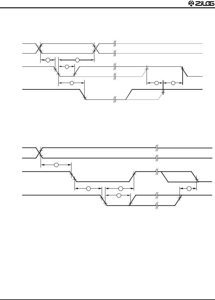
Handshake Timing Diagrams
Data In |
Data In Valid |
Next Data In Valid |
|
1 |
2 |
|
|
|
3 |
|
|
/DAV |
|
Delayed DAV |
|
(Input) |
|
|
|
|
4 |
5 |
6 |
RDY |
|
Delayed RDY |
|
(Output)
Figure 8. Input Handshake Timing
Data Out |
Data Out Valid |
|
Next Data Out Valid |
|
7 |
|
|
/DAV |
|
|
Delayed DAV |
(Output) |
|
|
|
|
8 |
9 |
11 |
|
|
10 |
|
RDY |
|
|
Delayed RDY |
(Input) |
|
|
|
Figure 9. Output Handshake Timing
12 |
DS96DZ80203 |

Z86C83/C84
Z8® MCU Microcontrollers
AC ELECTRICAL CHARACTERISTICS (Continued)
Handshake Timing Table
|
|
|
VCC |
TA = 0°C to +70°C TA = –40°C to +105°C |
Data |
|||
|
|
|
12 MHz |
16 MHz |
12 MHz |
16 MHz |
||
No |
Symbol |
Parameter |
Note1,2 |
Min Max Min Max Min Max |
Min Max |
Direction |
||
|
|
|
|
|
|
|
|
|
1 |
TsDI(DAV) |
Data In Setup Time |
3.0V |
0 |
0 |
0 |
0 |
IN |
|
|
|
|
|
|
|
|
|
|
|
|
5.5V |
0 |
0 |
0 |
0 |
IN |
|
|
|
|
|
|
|
|
|
2 |
ThDI(DAV) |
Data In Hold Time |
3.0V |
160 |
160 |
160 |
160 |
IN |
|
|
|
|
|
|
|
|
|
|
|
|
5.5V |
115 |
115 |
115 |
115 |
IN |
|
|
|
|
|
|
|
|
|
3 |
TwDAV |
Data Available Width |
3.0V |
155 |
155 |
155 |
155 |
IN |
|
|
|
|
|
|
|
|
|
|
|
|
5.5V |
110 |
110 |
110 |
110 |
IN |
|
|
|
|
|
|
|
|
|
4 |
TdDAVI(RDY) |
DAV Fall to RDY Fall Delay |
3.0V |
160 |
160 |
160 |
160 |
IN |
|
|
|
|
|
|
|
|
|
|
|
|
5.5V |
115 |
115 |
115 |
115 |
IN |
|
|
|
|
|
|
|
|
|
5 |
TdDAVId(RDY) |
DAV Rise to RDY Rise Delay |
3.0V |
120 |
120 |
120 |
120 |
IN |
|
|
|
|
|
|
|
|
|
|
|
|
5.5V |
80 |
80 |
80 |
80 |
IN |
|
|
|
|
|
|
|
|
|
6 |
TdRDY0(DAV) |
RDY Rise to DAV Fall Delay |
3.0V |
0 |
0 |
0 |
0 |
IN |
|
|
|
|
|
|
|
|
|
|
|
|
5.5V |
0 |
0 |
0 |
0 |
IN |
|
|
|
|
|
|
|
|
|
7 |
TdD0(DAV) |
Data Out to DAV Fall Delay |
3.0V |
42 |
31 |
42 |
31 |
OUT |
|
|
|
|
|
|
|
|
|
|
|
|
5.5V |
42 |
31 |
42 |
31 |
OUT |
|
|
|
|
|
|
|
|
|
8 |
TdDAV0(RDY) |
DAV Fall to RDY Fall Delay |
3.0V |
0 |
0 |
0 |
0 |
OUT |
|
|
|
|
|
|
|
|
|
|
|
|
5.5V |
0 |
0 |
0 |
0 |
OUT |
|
|
|
|
|
|
|
|
|
9 |
TdRDY0(DAV) |
RDY Fall to DAV Rise Delay |
3.0V |
160 |
160 |
160 |
160 |
OUT |
|
|
|
|
|
|
|
|
|
|
|
|
5.5V |
115 |
115 |
115 |
115 |
OUT |
|
|
|
|
|
|
|
|
|
10 |
TwRDY |
RDY Width |
3.0V |
110 |
110 |
110 |
110 |
OUT |
|
|
|
|
|
|
|
|
|
|
|
|
5.5V |
80 |
80 |
80 |
80 |
OUT |
|
|
|
|
|
|
|
|
|
11 |
TdRDY0d(DAV) |
RDY Rise to DAV Fall Delay |
3.0V |
110 |
110 |
110 |
110 |
OUT |
|
|
|
|
|
|
|
|
|
|
|
|
5.5V |
80 |
80 |
80 |
80 |
OUT |
|
|
|
|
|
|
|
|
|
Notes:
1.Timing Reference uses 0.7 VCC for a logic 1 and 0.2 VCC for a logic 0.
2.The VCC voltage specification of 3.0V guarantees 3.3V ±0.3V and the VCC voltage specification of 5.5V guarantees 5.0V ±0.5V.
13 |
DS96DZ80203 |

Z86C83/C84
Z8® MCU Microcontrollers
Table 5. D/A Converter Electrical Characteristics
VCC = 3.3V ± 10%
Parameter |
Minimum |
Typical |
Maximum |
Units |
|
|
|
|
|
Resolution |
|
8 |
|
Bits |
Integral non-linearity |
|
0.25 |
1 |
LSB |
Differential non-linearity |
|
0.25 |
0.5 |
LSB |
Setting time, 1/2 LSB |
|
1.5 |
3.0 |
sec |
Zero Error at 25°C |
|
10 |
20 |
mV |
Full Scale error at 25°C |
|
0.25 |
0.5 |
LSB |
Supply Range |
3.0 |
3.3 |
3.6 |
Volts |
Power dissipation, no load |
|
10 |
|
mW |
Ref Input resistance |
2K |
4K |
10K |
Ohms |
Output noise voltage |
|
50 |
|
Vp-p |
VDHI range at 3 volts |
1.5 |
1.8 |
2.1 |
Volts |
VDLO range at 3 volts |
0.2 |
0.5 |
0.8 |
Volts |
VDHI–VDLO, at 3 volts |
1.3 |
1.6 |
1.9 |
Volts |
Capacitive output load, CL |
|
|
20 |
pF |
Resistive output load, RL |
50K |
|
|
Ohms |
Output slew rate |
1.0 |
3.0 |
|
V/ sec |
|
|
|
|
|
Notes: |
|
|
|
|
Voltage: 3.0V to 3.6V |
|
|
|
|
Temp: 0–70°C |
|
|
|
|
|
|
|
||
|
Table 6. D/A Converter Electrical Characteristics |
|
||
|
VCC = 5.0V ±10% |
|
|
|
|
|
|
|
|
Parameter |
Minimum |
Typical |
Maximum |
Units |
|
|
|
|
|
Resolution |
|
8 |
|
Bits |
Integral non-linearity |
|
0.25 |
1 |
LSB |
Differential non-linearity |
|
0.25 |
0.5 |
LSB |
Setting time, 1/2 LSB |
|
1.5 |
3.0† |
sec |
Zero Error at 25°C |
|
10 |
20 |
mV |
Full Scale error at 25°C |
|
1 |
2 |
% FSR |
Supply Range |
4.5 |
5.0 |
5.5 |
Volts |
Power dissipation, no load |
|
50 |
85 |
mW |
Ref Input resistance |
2K |
4K |
10K |
Ohms |
Output noise voltage |
|
50 |
|
Vp-p |
VDHI range at 5 volts |
2.6 |
|
3.5 |
Volts |
VDLO range at 5V volts |
0.8 |
|
1.7 |
Volts |
VDHI–VDLO, at 5V volts |
0.9 |
|
2.7 |
Volts |
Capacitive output load, CL |
|
|
30 |
pF |
Resistive output load, RL |
20K |
|
|
Ohms |
Output slew rate |
1.0 |
3.0 |
|
V/ sec |
|
|
|
|
|
Notes:
Voltage: 4.5V - 5.5V
Temp: 0-70°C
† The C84 Emulator has maximum setting time of 20 sec. (10 sec. typical).
14 |
DS96DZ80203 |
Loading...