


 Loading...
PRELIMINARY PRODUCT SPECIFICATION
1
Z86318 |
1 |
Z8® MCU 8-BIT MICROCONTROLLER
FEATURES
|
ROM |
RAM* |
I/O |
Voltage |
Device |
(KB) |
(Bytes) |
Lines |
Range |
|
|
|
|
|
Z86318 |
124 |
14 |
21 |
0V to 6.0V |
|
|
|
|
|
Note: *General-Purpose
■–40°C to +105°C Operating Temperature Range
■Low-Power Consumption: 33 mW (Typical)
■ROM Mask Options:
– Permanent Watch-Dog Timer
–ROM Protect
–Low-Voltage Protection
–Pull-Up/Pull-Down I/O Pins (Nibble Programmable)
–Feedback Resistor on the On-Chip Oscillator
■On-Chip Oscillator (Crystal, Ceramic Resonator, LC, or External Clock Drive)
■Fast Instruction Pointer: 1.5 s @ 4 MHz
■ESD Protection Circuitry
GENERAL DESCRIPTION
The Z86318 is a member of the Z8® MCU family of CMOS microcontrollers. This device offers on-board pull-up and pull-down resistors (ROM mask-option programmable on a nibble basis), a scalable trip-point buffer to accommodate opto-transistor outputs, and high drive ports capable of up to 20 mA current sinking per pin (3 pins maximum).
The Z86318 features I/O Ports (IOL = 20 mA at VOL = 0.8V, 3 pins max.) to provide increased current sinking capabilities. These devices also offer users a selection of ROM mask options, which include a permanently enabled Watch-Dog Timer that ensures operational reliability across a broad range of application environments.
For applications requiring powerful I/O capabilities, the Z86318 provides dedicated input and output lines that are grouped into three ports. These ports can be configured by means of ROM mask options (nibble-programmable) as pull ups, pull downs, or neither. There are two basic address spaces available. Program Memory, and 124 bytes of general-purpose registers.
The Z86318 devices provide two on-chip 8-bit programmable counter/timers with a large number of user-selectable modes. Each counter/timer is driven by its own 6-bit programmable prescaler. The Z86318 counter/timers off-load system real-time tasks such as counting/timing and input/output data communications for increased system efficiency.
Notes: All Signals with a preceding front slash, “/”, are active Low, e.g.; B//W (WORD is active Low); /B/W (BYTE is active Low, only).
Power connections follow conventional descriptions below:
Connection |
Circuit |
Device |
|
|
|
Power |
VCC |
VDD |
|
|
|
Ground |
GND |
VSS |
|
|
|
DS96KEY0103 (8/96) |
P R E L I M I N A R Y |
1 |
Z86318
Z8® MCU 8-Bit Microcontroller
GENERAL DESCRIPTION (Continued)
Input |
VDD VSS |
XTAL |
|
|
|
|
|
|
|
|
|
|
|
|
|
|
|
|
|
|
|
|
|
|
|
|
|
|
|
|
|
|
|
|
|
|
|
|
|
|
|
|
|
|
|
|
|
|
|
|
|
|
|
|
|
|
|
|
|
|
|
|
|
|
|
|
|
|
|
|
|
|
|
|
|
|
|
|
|
|
|
|
|
|
|
|
|
|
|
|
|
|
|
|
|
|
|
|
|
|
|
|
|
|
|
|
|
|
|
|
|
|
|
|
|
|
|
|
|
|
|
|
|
|
|
|
|
|
|
|
|
|
|
|
|
|
|
|
|
|
|
|
|
|
|
|
|
|
|
|
|
|
|
|
|
|
|
|
Machine |
||||||||
|
|
|
|
|
|
|
|
|
|
|
|
|
|
|
|
|
|
|
|
|
|
|
|
|||||||||
Port 3 |
|
|
|
|
|
|
|
|
|
|
|
|
|
|
|
|
|
|
Timing & Inst. |
|||||||||||||
|
|
|
|
|
|
|
|
|
|
|
|
|
|
|
|
|
|
|||||||||||||||
|
|
|
|
|
|
|
|
|
|
|
|
|
|
|
|
|
|
|||||||||||||||
|
|
|
|
|
|
|
|
|
|
|
|
|
|
|
|
|
|
Control |
||||||||||||||
|
|
|
|
|
|
|
|
|
|
|
|
|
|
|
|
|
|
|
|
|
|
|
|
|||||||||
|
|
|
|
|
|
|
|
|
|
|
|
|
|
|
|
|
|
|
|
|
|
|
|
|
|
|
|
|
|
|
|
|
|
|
|
|
|
|
|
|
|
|
|
|
|
|
|
|
|
|
|
|
|
|
|
|
|
|
|
|
|
|
|
|
|
|
|
|
|
|
|
|
|
|
|
|
|
|
|
|
|
|
|
|
|
|
|
|
|
|
|
|
|
|
|
|
|
|
|
|
|
|
|
|
|
|
|
|
|
|
ALU |
|
|
|
|
|
|
|
|
|
|
|
|
|
|
|
|
||||
|
|
|
|
|
|
|
|
|
|
|
|
|
|
|
|
|
|
|
|
|
|
|
|
|
|
|
|
|||||
|
|
|
|
|
|
|
|
|
|
|
|
|
|
|
|
|
|
|
|
|
|
|
|
|
|
|
|
|||||
Counter/ |
|
|
|
|
|
|
|
|
|
|
|
|
|
|
|
|
|
|
Prg. Memory |
|||||||||||||
|
|
|
|
|
|
|
|
|
|
|
|
|
|
|
|
|
|
|||||||||||||||
Timers (2) |
|
|
|
|
|
|
|
|
|
|
|
|
|
|
|
|
|
|
||||||||||||||
|
|
|
|
|
FLAG |
|
|
|
|
|
|
|
3072 x 8-Bit (318) |
|||||||||||||||||||
|
|
|
|
|
|
|
|
|
|
|
|
|||||||||||||||||||||
|
|
|
|
|
|
|
|
|
|
|
|
|
|
|
|
|
|
|||||||||||||||
|
|
|
|
|
|
|
|
|
|
|
|
|
|
|
|
|
|
|
|
|
|
|
|
2048 x 8-Bit (319) |
||||||||
|
|
|
|
|
|
|
|
|
|
|
|
|
|
|
|
|
|
|
|
|
|
|
|
|||||||||
|
|
|
|
|
|
|
|
|
|
|
|
|
|
|
|
|
|
|
|
|
|
|
|
|
|
|
|
|
|
|
|
|
|
|
|
|
|
|
|
|
|
|
|
Register |
|
|
|
|
|
|
|
|
|
|
|
|
|
|
|
||||||
Interrupt |
|
|
|
|
|
Pointer |
|
|
|
|
|
|
Program |
|||||||||||||||||||
|
|
|
|
|
|
|
|
|
|
|
|
|
|
|
|
|
|
|||||||||||||||
|
|
|
|
|
|
|
|
|
|
|
|
|
|
|
|
|
|
|||||||||||||||
Control |
|
|
|
|
|
|
|
|
|
|
|
|
|
|
|
|
|
|
Counter |
|||||||||||||
|
|
|
|
Register File |
|
|
|
|
|
|
|
|||||||||||||||||||||
|
|
|
|
|
|
|
|
|
|
|
|
|
|
|
|
|
|
|
|
|
|
|
|
|
||||||||
|
|
|
|
|
|
|
|
|
|
144 x 8-Bit |
|
|
|
|
|
|
|
|
|
|
|
|
|
|
|
|||||||
|
|
|
|
|
|
|
|
|
|
|
|
|
|
|
|
|
|
|
|
|
|
|
|
|
|
|||||||
|
|
|
|
|
|
|
|
|
|
|
|
|
|
|
|
|
|
|
|
|
|
|
|
|
|
|
|
|
|
|
|
|
|
|
|
|
|
|
|
|
|
|
|
|
|
|
|
|
|
|
|
|
|
|
|
|
|
|
|
|
|
|
|
|
|
|
|
|
|
|
|
|
|
|
|
|
|
|
|
|
|
|
|
|
|
|
|
|
|
|
|
|
|
|
|
|
|
|
|
|
|
|
|
|
|
|
|
|
|
|
|
|
|
|
|
|
|
|
|
|
|
|
|
|
|
|
|
|
|
|
|
|
|
|
|
|
|
|
|
|
|
|
|
|
|
|
|
|
|
|
|
|
|
|
|
|
|
|
|
|
|
|
|
|
|
|
|
|
|
|
|
|
|
|
|
|
|
|
|
|
|
|
|
|
|
|
|
|
|
|
|
|
|
|
|
|
|
|
|
|
|
|
|
|
|
|
|
|
|
|
|
|
|
|
|
|
|
|
|
|
|
|
|
|
|
|
|
|
|
|
|
|
|
|
|
|
|
|
|
|
|
|
|
|
|
|
|
|
|
|
|
|
|
|
|
|
|
|
|
|
|
|
|
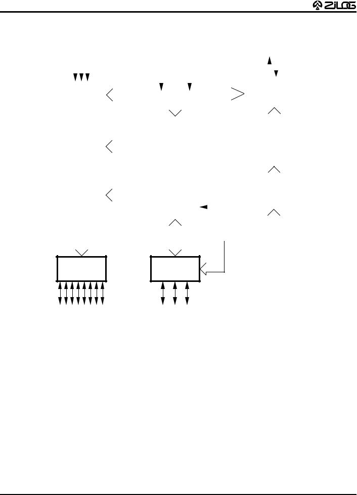
Port 2 |
Port 0 |
I/O I/O
(Bit Programmable)
Figure 1. Z86318 Functional Block Diagram
2 |
P R E L I M I N A R Y |

Z86318
Z8® MCU 8-Bit Microcontroller
PIN DESCRIPTIONS
P24 |
|
1 |
18 |
|
P23 |
Table 1. Z86318 18 Pin DIP/SOIC Pin Identification |
|||
|
|
||||||||
P25 |
|
2 |
17 |
|
P22 |
||||
|
|
|
|
|
|
||||
|
|
Pin # |
Symbol |
Function |
Direction |
||||
P26 |
|
3 |
16 |
|
P21 |
||||
|
|
|
|
|
|
||||
|
|
1-4 |
P24-P27 |
Port 2, Pins 4, 5, 6, 7 |
In/Output |
||||
P27 |
|
|
|
|
|
||||
|
4 |
15 |
|
P20 |
5 |
VDD |
Power Supply |
Input |
|
|
|
||||||||
VDD |
|
5 |
Z86318 14 |
|
VSS |
6 |
XTAL2 |
XTAL Osc. Clock |
Output |
XTAL2 |
|
6 |
13 |
|
P02 |
7 |
XTAL1 |
XTAL Osc. Clock |
Input |
|
|
||||||||
|
|
8 |
P31 |
Port 3, Pin 1 |
Input |
||||
XTAL1 |
|
|
|
|
|
||||
|
7 |
12 |
|
P01 |
9 |
P32 |
Port 3, Pin 2 |
Input |
|
P31 |
|
8 |
11 |
|
P00 |
10 |
P33 |
Port 3, Pin 3 |
Input |
|
|
||||||||
|
|
11-13 |
P00-P02 |
Port 0, Pins 0, 1, 2 |
In/Output |
||||
P32 |
|
9 |
10 |
|
P33 |
||||
|
|
14 |
VSS |
Ground |
|
||||
|
|
|
|
||||||
|
|
|
|
|
|
15-18 |
P20-P23 |
Port 2, Pins 0, 1, 2, 3 |
In/Output |
|
|
|
|
|
|
|
|
|
|
Figure 2. Z86318 18-Pin DIP/SOIC
Pin Configuration
ABSOLUTE MAXIMUM RATINGS
Sym. |
Parameter |
Min. |
Max. |
Units |
|
|
|
|
|
VDD |
Supply Voltage* |
–0.3 |
+7 |
V |
TSTG |
Storage Temp. |
–65° |
+150° |
C |
TA |
Oper. Ambient Temp. |
† |
† |
C |
Note: |
|
|
|
|
*Voltages on all pins with respect to Ground. †See Ordering Information.
Stresses greater than those listed under Absolute Maximum Ratings may cause permanent damage to the device. This is a stress rating only; operation of the device at any condition above those indicated in the operational sections of these specifications is not implied. Exposure to absolute maximum rating conditions for extended periods may affect device reliability.
P R E L I M I N A R Y |
3 |
Z86318
Z8® MCU 8-Bit Microcontroller
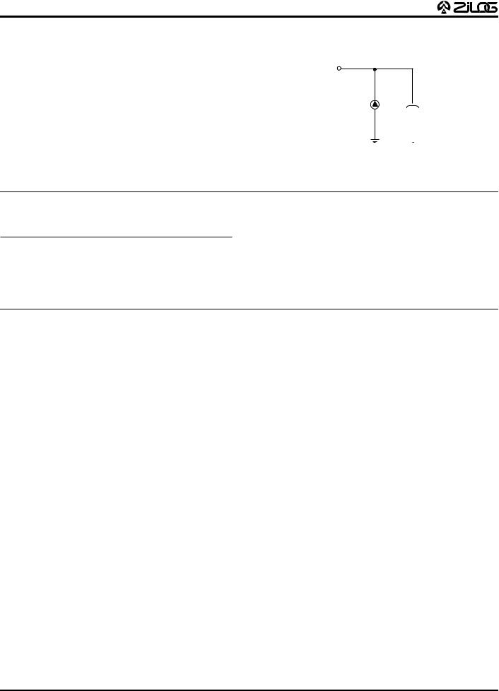
STANDARD TEST CONDITIONS
The characteristics listed below apply for standard test conditions as noted. All voltages are referenced to Ground.Positive current flows into the referenced pin (Figure 3).
From Output
Under Test
I |
|
|
|
|
|
|
|
150 pF |
|
|
|
|
|
|
|
||
|
||||||||
|
|
|
|
|
|
|
|
|
|
|
|
|
|
|
|
|
|
Figure 3. Test Load Diagram
CAPACITANCE
TA = GND = 0V, f = 1.0 MHz, unmeasured pins returned to Ground.
Parameter |
Min. |
Max. |
|
|
|
Input Capacitance |
0 |
10 pF |
|
|
|
Output Capacitance |
0 |
20 pF |
|
|
|
I/O Capacitance |
0 |
25 pF |
|
|
|
VCC SPECIFICATION
VCC = 4.0V to 6.0V
4 |
P R E L I M I N A R Y |

Z86318
Z8® MCU 8-Bit Microcontroller
DC ELECTRICAL CHARACTERISTICS
|
|
|
TA= 0°C to +70°C |
Typical |
|
|
|
Sym |
Parameter |
VDD |
Min |
Max |
@ 25°C |
Units |
Conditions |
|
Max Input Voltage |
4.0V |
|
12 |
|
V |
VIN < 250 A (Port Pins Only) |
VCH |
Clock Input High |
4.0V |
0.7 VDD |
VDD + 0.3 |
2.0 |
V |
Driven by External Clock Generator |
|
Voltage |
6.0V |
0.7 VDD |
VDD + 0.3 |
3.0 |
V |
|
VCL |
Clock Input Low |
4.0V |
VSS – 0.3 |
0.2 VDD |
0.8 |
V |
Driven by External Clock Generator |
|
Voltage |
6.0V |
VSS – 0.3 |
0.2 VDD |
1.5 |
V |
|
VIH |
Input High Voltage |
4.0V |
0.7 VDD |
VDD + 0.3 |
1.6 |
V |
|
|
Schmitt-Triggered |
6.0V |
0.7 VDD |
VDD + 0.3 |
2.6 |
V |
|
VIH |
Input High Voltage |
4.0V |
0.7 VDD |
VDD + 0.3 |
1.4 |
V |
|
|
CMOS Input |
6.0V |
0.7 VDD |
VDD + 0.3 |
2.6 |
V |
|
VIL |
Input Low Voltage |
4.0V |
VSS – 0.3 |
0.2 VDD |
0.8 |
V |
|
|
Schmitt-Triggered |
6.0V |
VSS – 0.3 |
0.2 VDD |
1.5 |
V |
|
VIL |
Input Low Voltage |
4.0V |
VSS – 0.3 |
0.2 VDD |
1.3 |
V |
|
|
CMOS Input |
6.0V |
VSS – 0.3 |
0.2 VDD |
2.4 |
V |
|
VOH |
Output High |
4.0V |
VDD – 0.4 |
|
2.8 |
V |
IOH = –2.0 mA |
|
Voltage |
4.5V |
VDD – 0.4 |
|
4.4 |
V |
|
VOL1 |
Output Low Voltage |
4.0V |
|
0.6 |
0.2 |
V |
IOL = +4.0 mA |
|
|
6.0V |
|
0.4 |
0.1 |
V |
|
|
|
|
|
|
|
|
|
VOL2 |
Output Low Voltage |
4.0V |
|
1.5 |
0.8 |
V |
IOL = 20.0 mA, 3 Pin Max |
|
|
6.0V |
|
0.8 |
0.3 |
V |
OL = 10.0 mA, 6 Pin Max |
VLV |
VCC Low-Voltage |
|
1.6 |
2.7 |
2.3 |
V |
@ 2 MHz Max |
|
Protection* |
|
|
|
|
|
|
VTP |
Trip-Point Voltage* |
4.0V |
|
0.4 VDD |
|
V |
P24-P27 |
|
|
4.5V |
1.5 |
2.1 |
1.8 |
V |
|
|
|
|
|
|
|
|
|
|
|
5.5V |
1.9 |
2.5 |
2.2 |
V |
|
|
|
6.0V |
2.1 |
2.7 |
2.4 |
V |
|
|
|
|
|
|
|
|
|
VOC |
Input Open-Circuit |
4.5V |
0.95 |
1.15 |
1.04 |
V |
No Off-Chip Resistance |
|
Voltage |
5.0V |
1.05 |
1.25 |
1.15 |
V |
|
|
|
|
|
|
|
|
|
|
|
5.5V |
1.15 |
1.39 |
1.27 |
V |
|
|
|
6.0V |
1.25 |
1.49 |
1.37 |
V |
|
|
|
|
|
|
|
|
|
IIL |
Input Leakage |
3.0V |
–1.0 |
1.0 |
0.4 |
A |
VIN = 0V, VCC |
|
|
5.5V |
–1.0 |
1.0 |
0.4 |
A |
|
|
|
6.0V |
–1.0 |
1.0 |
0.4 |
A |
|
|
|
|
|
|
|
|
|
IOL |
Output Leakage |
4.0V |
–1.0 |
1.0 |
0.4 |
A |
VIN = 0V, VCC |
|
|
5.5V |
–1.0 |
1.0 |
0.4 |
A |
|
|
|
6.0V |
–1.0 |
1.0 |
0.4 |
A |
|
|
|
|
|
|
|
|
|
Note:
*The Z86318 is functional to VLV voltage. The minimum operational VDD is determined by the value of the VLV voltage at ambient temperature. The VLV voltage increases as temperature decreases.
P R E L I M I N A R Y |
5 |

Z86318
Z8® MCU 8-Bit Microcontroller
DC ELECTRICAL CHARACTERISTICS (Continued)
|
|
|
TA= 0°C to +70°C |
Typical |
|
|
|
|
Sym. |
Parameter |
VDD |
Min. |
Max. |
@ 25°C |
Units Conditions |
Notes |
|
IDD |
Supply Current |
4.0V |
|
1.5 |
0.41 |
mA |
@ 1 MHz |
[1] |
|
|
4.0V |
|
2.0 |
0.93 |
mA |
@ 2 MHz |
[1] |
|
|
4.0V |
|
3.0 |
1.64 |
mA |
@ 4 MHz |
[1] |
|
|
|
|
|
|
|
|
|
|
|
6.0V |
|
3.0 |
1.44 |
mA |
@ 1 MHz |
[1] |
|
|
6.0V |
|
4.0 |
2.60 |
mA |
@ 2 MHz |
[1] |
|
|
6.0V |
|
6.0 |
4.28 |
mA |
@ 4 MHz |
[1] |
|
|
|
|
|
|
|
|
|
IDD1 |
Standby Current |
4.0V |
|
0.6 |
0.15 |
mA |
HALT mode VIN = 0V, VCC @ 1 MHz |
|
|
|
4.0V |
|
0.8 |
0.20 |
mA |
HALT mode VIN = 0V, VCC @ 2 MHz |
|
|
|
4.0V |
|
1.0 |
0.3 |
mA |
HALT mode VIN = 0V, VCC @ 4 MHz |
|
|
|
|
|
|
|
|
||
|
|
6.0V |
|
1.3 |
0.70 |
mA |
HALT mode VIN = 0V, VCC @ 1 MHz |
|
|
|
6.0V |
|
1.5 |
0.80 |
mA |
HALT mode VIN = 0V, VCC @ 2 MHz |
|
|
|
6.0V |
|
2.0 |
1.0 |
mA |
HALT mode VIN = 0V, VCC @ 4 MHz |
|
|
|
|
|
|
|
|
||
IDD2 |
Standby Current |
6.0V |
|
10 |
1.5 |
mA |
STOP mode VIN = 0V, VCC |
|
IPU |
Pull-Up Current (100K) |
4.5V |
-20 |
|
|
A |
VIH @ 1V |
|
|
Port P00–P02; |
6.0V |
|
105 |
|
|
VIH @ 1V |
|
|
Port P22, P23; |
|
|
|
|
|
|
|
|
Port P31–P33 |
|
|
|
|
|
|
|
|
|
|
|
|
|
|
|
|
IPD |
Pull-Down Current (100K) |
4.5V |
20 |
|
|
A |
VIL @ 3V |
|
|
Port P00–P02; |
6.0V |
|
114 |
|
|
VIL @ 4V |
|
|
Port P22, P23; |
|
|
|
|
|
|
|
|
Port P31–P33 |
|
|
|
|
|
|
|
|
|
|
|
|
|
|
|
|
IPU |
Pull-Up Current (10K) |
4.5V |
208 |
|
|
A |
VIH @ 0V |
|
|
Port P20, P21 |
6.0V |
|
870 |
|
|
VIH @ 0V |
|
IPD |
Pull-Down Current (10K) |
4.5V |
170 |
|
|
A |
VIH @ 3V |
|
|
Port P20, P21 |
6.0V |
|
870 |
|
|
VIH @ 3V |
|
Note: [1] All outputs unloaded, I/O pins floating, inputs at rail.
6 |
P R E L I M I N A R Y |

Z86318
Z8® MCU 8-Bit Microcontroller
AC ELECTRICAL CHARACTERISTICS
Timing Diagrams
1 |
3 |
Clock
2 |
2 |
3 |
7 7
TIN
4 5
6
IRQ N
8 |
9 |
Figure 4. Electrical Timing Diagram
P R E L I M I N A R Y |
7 |

Z86318
Z8® MCU 8-Bit Microcontroller
AC ELECTRICAL CHARACTERISTICS
(VDD = 4V to 6V ±10%, TA = 0°C to +70°C, unless otherwise specified)
|
|
|
|
|
TA = 0°C to +70°C |
|
|
|
|
|
|
|
|
1 MHz |
4 MHz |
|
|
||
No. |
Symbol |
Parameter |
VDD |
Min. |
Max. |
Min. |
Max. |
Units |
Notes |
1 |
TpC |
Input Clock Period |
6.0V |
1,000 |
100,000 |
250 |
100,000 |
ns |
[1] |
|
|
|
|
|
|
|
|
|
|
2 |
TrC,TfC |
Clock Input Rise |
6.0V |
|
25 |
|
25 |
ns |
|
|
|
and Fall Times |
|
|
|
|
|
|
|
|
|
|
|
|
|
|
|
|
|
3 |
TwC |
Input Clock Width |
6.0V |
|
475 |
|
100 |
ns |
[1] |
|
|
|
|
|
|
|
|
|
|
4 |
TwTinL |
Timer Input Low Width |
6.0V |
|
70 |
|
70 |
ns |
[1] |
|
|
|
|
|
|
|
|
|
|
5 |
TwTinH |
Timer Input High Width |
6.0V |
2.5TpC |
|
2.5TpC |
|
|
[1] |
|
|
|
|
|
|
|
|
|
|
6 |
TpTin |
Timer Input Period |
6.0V |
4TpC |
|
4TpC |
|
|
[1] |
|
|
|
|
|
|
|
|
|
|
7 |
TrTin, |
Timer Input Rise |
6.0V |
|
100 |
|
100 |
ns |
[1] |
|
TtTin |
and Fall Timer |
|
|
|
|
|
|
|
|
|
|
|
|
|
|
|
|
|
8 |
TwIL |
Int. Request Input |
6.0V |
70 |
|
70 |
|
ns |
[1,2] |
|
|
Low Time |
|
|
|
|
|
|
|
|
|
|
|
|
|
|
|
|
|
9 |
TwIH |
Int. Request Input |
6.0V |
2.5TpC |
|
2.5TpC |
|
|
[1,2] |
|
|
High Time |
|
|
|
|
|
|
|
|
|
|
|
|
|
|
|
|
|
10 |
Twdt |
Watch-Dog Timer |
6.0V |
24 |
|
24 |
|
ms |
|
|
|
|
|
|
|
|
|
|
|
11 |
TPOR |
Power-On Reset Time |
6.0V |
6 |
|
6 |
|
ms |
[1] |
Notes:
1.Timing Reference uses 0.9 VDD for a logic 1 and 0.1 VDD for a logic 0.
2.Interrupt request through Port 3 (P33-P31).
8 |
P R E L I M I N A R Y |
Loading...