


Z8018006PSC
ZILOG Z8018006PSC, Z8018006VEC, Z8018006VSC, Z8018008FEC, Z8018008FSC Datasheet
...
DS971800401
P R E L I M I N A R Y
1-1
1
P
RELIMINARY
P
RODUCT
S
PECIFICATION
Z80180/Z8S180/
1
Z8L180 SL1919
E
NHANCED
Z180 M
ICROPROCESSOR
FEATURES
■
Code Compatible with Zilog Z80
®
CPU
■
Extended Instructions
■
Two Chain-Linked DMA Channels
■
Low Power-Down Modes
■
On-Chip Interrupt Controllers
■
Three On-Chip Wait-State Generators
■
On-Chip Oscillator/Generator
■
Expanded MMU Addressing (up to 1 MB)
■
Clocked Serial I/O Port
■
Two 16-Bit Counter/Timers
■
Two Enhanced UARTs (up to 512 Kbps)
■
Clock Speeds: 6, 8, 10, 20, 33 MHz
■
Operating Range: 5V (3.3V@ 20 MHz)
■
Operating Temperature Range: 0
°
C to +70
°
C
■
-40
°
C to +85
°
C Extended Temperature Range
■
Three Packaging Styles
– 68-Pin PLCC
– 64-Pin DIP
– 80-Pin QFP
GENERAL DESCRIPTION
The enhanced Z80180/Z8S180/Z8L180
™
significantly im-
proves on the previous Z80180 models while still providing
full backward compatibility with existing Zilog Z80 devices.
The Z80180/Z8S180/Z8L180 now offers faster execution
speeds, power saving modes, and EMI noise reduction.
This enhanced Z180 design also incorporates additional
feature enhancements to the ASCIs, DMAs, and I
cc
STANDBY Mode power consumption. With the addition of
“ESCC-like” Baud Rate Generators (BRGs), the two ASCIs
now have the flexibility and capability to transfer data asyn-
chronously at rates of up to 512 Kbps. In addition, the ASCI
receiver has added a 4-byte First In First Out (FIFO) which
can be used to buffer incoming data to reduce the inci-
dence of overrun errors. The DMAs have been modified to
allow for a “chain-linking” of the two DMA channels when
set to take their DMA requests from the same peripherals
device. This feature allows for non-stop DMA operation be-
tween the two DMA channels, reducing the amount of CPU
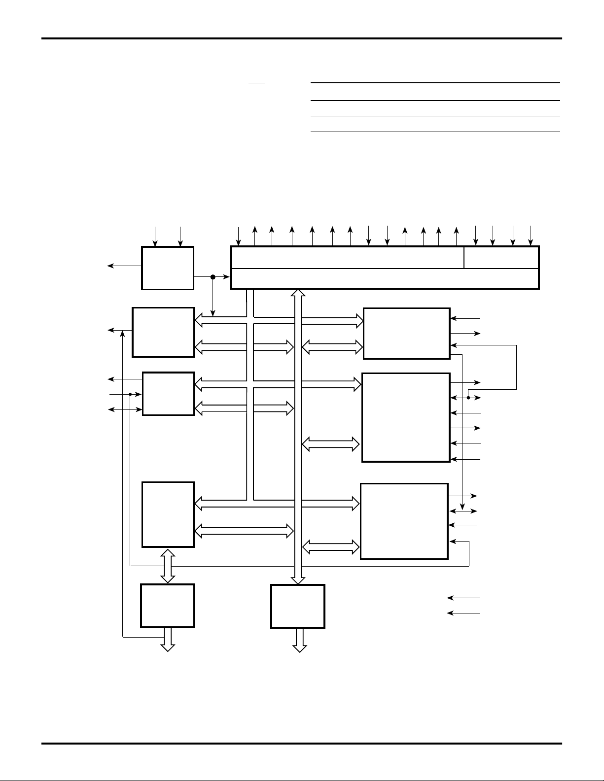
intervention (Figure 1).
Not only does the Z80180/Z8S180/Z8L180 consume less
power during normal operations than the previous model,
it has also been designed with three modes intended to fur-
ther reduce the power consumption. Zilog reduced I
cc
pow-
er consumption during STANDBY Mode to a minimum of
10
µ
A by stopping the external oscillators and internal
clock. The SLEEP mode reduces power by placing the
CPU into a “stopped” state, thereby consuming less cur-
rent while the on-chip I/O device is still operating. The
SYSTEM STOP mode places both the CPU and the on-
chip peripherals into a “stopped” mode, thereby reducing
power consumption even further.
A new clock doubler feature has been implemented in the
Z80180/Z8S180/Z8L180 device that allows the program-
mer to double the internal clock from that of the external
clock. This provides a systems cost savings by allowing
the use of lower cost, lower frequency crystals instead of
the higher cost, and higher speed oscillators.
The Enhanced Z180 is housed in 80-pin QFP, 68-pin
PLCC, and 64-pin DIP packages.
Z80180/Z8S180/Z8L180
Enhanced Z180 Microprocessor Zilog
1-2
P R E L I M I N A R Y
DS971800401
Notes:
All Signals with a preceding front slash, “/” are ac-
tive Low, for example, B//W (WORD is active Low); /B/W
(BYTE is active Low, only). Alternatively, an overslash
may be used to signify active Low, for example WR
Power connections follow conventional descriptions be-
low:
Connection Circuit Device
Power V
CC
V
DD
Ground GND V
SS
Figure 1. Z80180/Z8S180/Z8L180 Functional Block Diagram
16-bit
Programmable
Reload Timers
(2)
Clocked
Serial I/O
Port
MMU
Bus State Control
CPU
Interrupt
/RESET
/RD
/WR
/M1
/MREQ
IORQ
/HALT
/WAIT
/BUSREQ
/BUSACK
/RFSH
ST
E
/NMI
INT0
INT1
INT2
TXS
RXS/CTS1
CKS
A18/TOUT
DMACS
(2)
Asynchronous
SCI
(Channel 0)
Asynchronous
SCI
(Channel 1)
/DREQ1
TEND1
TXA0
CKA0, /DREQ0
RXA0
/RTS0
/CTS0
/DCD0
TXA1
CKA1, /TEND0
RXA1
Timing
Generator
XTAL
EXTAL
Ø
Data
Buffer
Address
Buffer
VCC
VSS
A19-A0
D7-D0
Data Bus (8-Bit)
Address Bus (16-Bit)
Z80180/Z8S180/Z8L180
Zilog Enhanced Z180 Microprocessor
DS971800401
P R E L I M I N A R Y
1-3
1
PIN DESCRIPTION
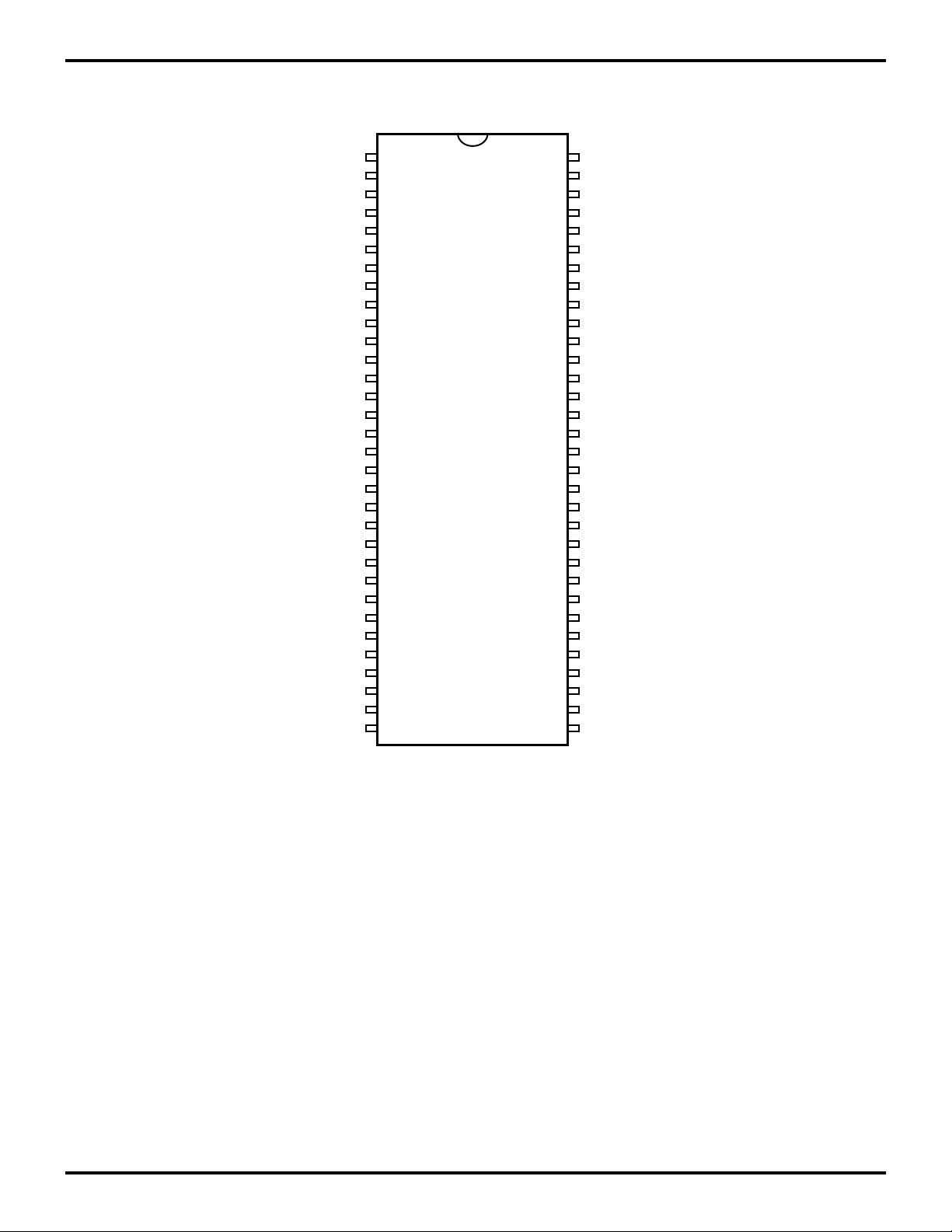
Figure 2. Z80180 64-Pin DIP Pin Configuration
VSS
XTAL
EXTAL
/WAIT
/BUSACK
/BUSREQ
/RESET
/NMI
/INT0
/INT1
/INT2
ST
A0
A1
A2
A3
A4
A5
A6
A7
A8
A9
A10
A11
A12
A13
A14
A15
A16
A17
A18/TOUT
VCC
PHI
/RD
/WR
/M1
E
/MREQ
/IORQ
/RFSH
/HALT
/TEND1
/DREQ
CKS
RXS//CTS
TXS
CKA1//TEND0
RXA1
TXA1
CKA//DREQ0
RXA0
TXA0
/DCD0
/CTS0
/RTS0
D7
D6
D5
D4
D3
D2
D1
D0
VSS
33
64
Z80180 64-
Pin DIP
32
1
Z80180/Z8S180/Z8L180
Enhanced Z180 Microprocessor Zilog
1-4
P R E L I M I N A R Y
DS971800401
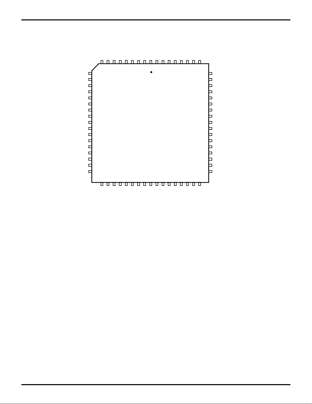
Figure 3. Z80180/Z8S180/Z8L180 68-Pin PLCC Pin Configuration
6010
/INT0
/INT1
/INT2
ST
A0
A1
A2
A3
VSS
A4
A5
A6
A7
A8
A9
A10
A11
/NMI
/RESET
/BUSREQ
/BUSACK
/WAIT
EXTAL
XTAL
VSS
VSS
PHI
/RD
/WR
/M1
E
/MREQ
/IORQ
/RFSH
4327
619
Z80180/Z8S180/
Z8L180
68-Pin PLCC
1
/HALT
/TEND1
/DREQ1
CKS
RXS//CTS1
TXS
CKA1//TEND0
RXA1
TEST
TXA1
CKA0//DREQ0
RXA0
TXA0
/DCD0
/CTS0
/RTS0
D7
A12
A13
A14
A15
A16
A17
A18/TOUT
VCC
A19
VSS
D0
D1
D2
D3
D4
D5
D6
Z80180/Z8S180/Z8L180
Zilog Enhanced Z180 Microprocessor
DS971800401
P R E L I M I N A R Y
1-5
1
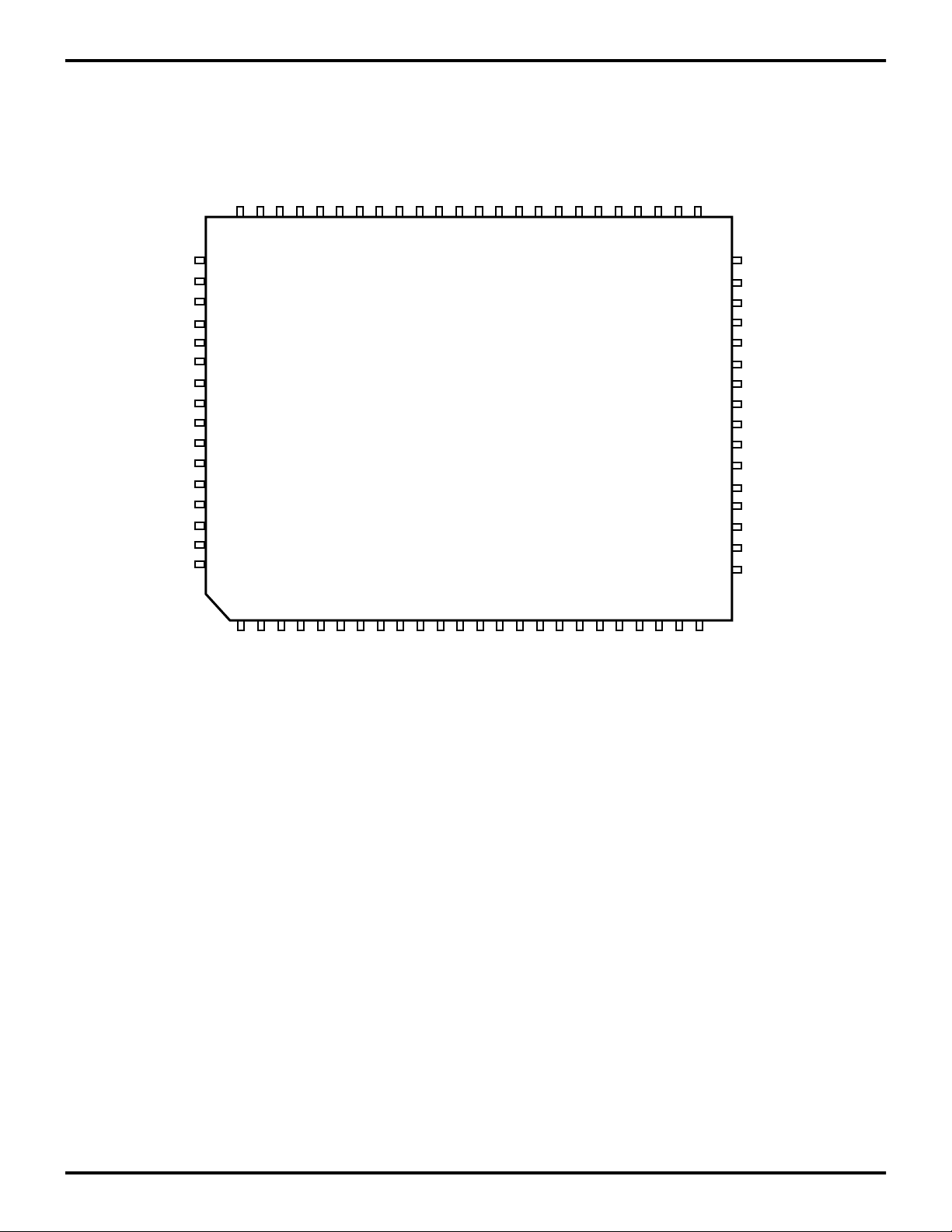
Figure 4. Z80180/Z8S180/Z8L180 80-Pin QFP Pin Configuration
40
65
/IORQ
/MREQ
E
/M1
/WR
/RD
PHI
VSS
VSS
XTAL
N/C
EXTAL
/WAIT
/BUSACK
/BUSREQ
/RESET
/NMI
N/C
N/C
/INT0
/INT1
/INT2
ST
A0
A1
A2
A3
VSS
A4
N/C
A5
A6
A7
A8
A9
A10
A11
N/C
N/C
A12
/RFSH
N/C
N/C
/HALT
/TEND1
/DREQ1
CKS
RXS/CTS1
TXS
CKA1//TEND0
RXA1
TEST
TXA1
N/C
CKA0//DREQ0
RXA0
TXA0
/DCD0
/CTS0
/RTS0
D7
N/C
N/C
D6
5101520
24
60
55 50 45 4164
Z80180/Z8S180/Z8L180
80-Pin QFP
1
D5
D4
D3
D2
D1
D0
VSS
A19
VCC
A18/TOUT
NC
A17
A16
A15
A14
A13

Z80180/Z8S180/Z8L180
Enhanced Z180 Microprocessor Zilog
1-6
P R E L I M I N A R Y
DS971800401
Table 1. Z80180/Z8S180/Z8L180 Pin Identification
Pin Number and Package Type
Default Function
Secondary
Function ControlQFP PLCC DIP
1 9 8 /NMI
2NC
3NC
4 10 9 /INT0
5 11 10 /INT1
6 12 11 /INT2
71312 ST
81413 A0
91514 A1
10 16 15 A2
11 17 16 A3
12 18 V
SS
13 19 17 A4
14 NC
15 20 18 A5
16 21 19 A6
17 22 20 A7
18 23 21 A8
19 24 22 A9
20 25 23 A10
21 26 24 A11
22 NC
23 NC
24 27 25 A12
25 28 26 A13
26 29 27 A14
27 30 28 A15
28 31 29 A16
29 32 30 A17
30 NC
31 33 31 A18 /T
OUT
Bit 2 or Bit 3 of TCR
32 34 32 V
CC
33 35 A19
34 36 33 V
SS
35 37 34 D0
36 38 35 D1
37 39 36 D2
38 40 37 D3
39 41 38 D4
40 42 39 D5
41 43 40 D6
42 NC
43 NC
44 44 41 D7
45 45 42 /RTS0

Z80180/Z8S180/Z8L180
Zilog Enhanced Z180 Microprocessor
DS971800401
P R E L I M I N A R Y
1-7
1
46 46 43 /CTS0
47 47 44 /DCD0
48 48 45 TXA0
49 49 46 RXA0
50 50 47 CKA0 /DREQ0 Bit 3 or Bit 5 of DMODE
51 NC
52 51 48 TXA1
53 52 TEST
54 53 49 RXA1
55 54 50 CKA1 /TEND0 Bit 4 of CNTLA1
56 55 51 TXS
57 56 52 RXS /CTS1 Bit 2 of STAT1
58 57 53 CKS
59 58 54 /DREQ1
60 59 55 /TEND1
61 60 56 /HALT
62 NC
63 NC
64 61 57 /RFSH
65 62 58 /IORQ
66 63 59 /MREQ
67 64 60 E
68 65 61 M1
69 66 62 /WR
70 67 63 /RD
71 68 64 PHI
72 1 1 V
SS
73 2 V
SS
74 3 2 XTAL
75 NC
76 4 3 EXTAL
77 5 4 /WAIT
78 6 5 /BUSACK
79 7 6 /BUSREQ
80 8 7 /RESET
Table 1. Z80180/Z8S180/Z8L180 Pin Identification
Pin Number and Package Type
Default Function
Secondary
Function ControlQFP PLCC DIP

Z80180/Z8S180/Z8L180
Enhanced Z180 Microprocessor Zilog
1-8
P R E L I M I N A R Y
DS971800401
Table 2. Pin Status During RESET BUSACK and SLEEP
Pin Number and Package Type Pin Status
QFP PLCC DIP
Default
Function
Secondary
Function RESET BUSACK
SLEEP
1 9 8 /NMI IN IN IN
2NC
3NC
4 10 9 /INT0 IN IN IN
5 11 10 /INT1 IN IN IN
6 12 11 /INT2 IN IN IN
71312ST 1?1
81413A0 3T 3T 1
91514A1 3T 3T 1
10 16 15 A2 3T 3T 1
11 17 16 A3 3T 3T 1
12 18 V
SS
GND GND GND
13 19 17 A4 3T 3T 1
14 NC
15 20 18 A5 3T 3T 1
16 21 19 A6 3T 3T 1
17 22 20 A7 3T 3T 1
18 23 21 A8 3T 3T 1
19 24 22 A9 3T 3T 1
20 25 23 A10 3T 3T 1
21 26 24 A11 3T 3T 1
22 NC
23 NC
24 27 25 A12 3T 3T 1
25 28 26 A13 3T 3T 1
26 29 27 A14 3T 3T 1
27 30 28 A15 3T 3T 1
28 31 29 A16 3T 3T 1
29 32 30 A17 3T 3T 1
30 NC
31 33 31 A18 /T
OUT
3T 3T 1
32 34 32 V
CC
V
CC
V
CC
V
CC
33 35 A19 3T 3T 1
34 36 33 V
SS
GND GND GND
35 37 34 D0 3T 3T 3T
36 38 35 D1 3T 3T 3T
37 39 36 D2 3T 3T 3T
38 40 37 D3 3T 3T 3T
39 41 38 D4 3T 3T 3T
40 42 39 D5 3T 3T 3T
41 43 40 D6 3T 3T 3T
42 NC
43 NC
44 44 41 D7 3T 3T 3T
Z80180/Z8S180/Z8L180
Zilog Enhanced Z180 Microprocessor
DS971800401
P R E L I M I N A R Y
1-9
1
45 45 42 /RTS0 1 OUT 1
46 46 43 /CTS0 IN OUT IN
47 47 44 /DCD0 IN IN IN
48 48 45 TXA0 1 OUT OUT
49 49 46 RXA0 IN IN IN
50 50 47 CKA0 /DREQ0
3T OUT OUT
51 NC
52 51 48 TXA1 1 OUT OUT
53 52 TEST
54 53 49 RXA1 IN IN IN
55 54 50 CKA1 /TEND0
3T IN IN
56 55 51 TXS 1 OUT OUT
57 56 52 RXS /CTS1 IN IN IN
58 57 53 CKS 3T I/O I/O
59 58 54 /DREQ1 IN 3T IN
60 59 55 /TEND1 1 OUT 1
61 60 56 /HALT 1 1 0
62 NC
63 NC
64 61 57 /RFSH 1 OUT OUT
65 62 58 /IORQ 1 3T 1
66 63 59 /MREQ 1 3T 1
67 64 60 E 0 OUT OUT
68 65 61 /M1 1 1 1
69 66 62 /WR 1 3T 1
70 67 63 /RD 1 3T 1
71 68 64 PHI OUT OUT OUT
72 1 1 V
SS
GND GND GND
73 2 V
SS
GND GND GND
74 3 2 XTAL OUT OUT OUT
75 NC
76 4 3 EXTAL IN IN IN
77 5 4 /WAIT IN IN IN
78 6 5 /BUSACK 1 OUT OUT
79 7 6 /BUSREQ IN IN IN
80 8 7 /RESET IN IN IN
Table 2. Pin Status During RESET BUSACK and SLEEP
Pin Number and Package Type Pin Status
QFP PLCC DIP
Default
Function
Secondary
Function RESET BUSACK
SLEEP

Z80180/Z8S180/Z8L180
Enhanced Z180 Microprocessor Zilog
1-10
P R E L I M I N A R Y
DS971800401
PIN DESCRIPTIONS
A0-A19.
Address Bus (Output, active High, tri-state). A0-
A19 form a 20-bit address bus. The Address Bus provides
the address for memory data bus exchanges, up to 1 MB,
and I/O data bus exchanges, up to 64K. The address bus
enters a high-impedance state during reset and external
bus acknowledge cycles. Address line A18 is multiplexed
with the output of PRT channel 1 (T
OUT
, selected as ad-
dress output on reset) and address line A19 is not avail-
able in DIP versions of the Z80180.
BUSACK.
Bus Acknowledge (Output, active Low).
/BUSACK indicated the requesting device, the MPU ad-
dress and data bus, and some control signals, have en-
tered their high-impedance state.
/BUSREQ.
Bus Request (Input, active Low). This input is
used by external devices (such as DMA controllers) to re-
quest access to the system bus. This request has a higher
priority than /NMI and is always recognized at the end of
the current machine cycle. This signal will stop the CPU
from executing further instructions and places address and
data buses, and other control signals, into the high-imped-
ance state.
CKA0, CKA1.
Asynchronous Clock 0 and 1 (Bidirectional,
active High). When in output mode, these pins are the
transmit and receive clock outputs from the ASCI baud
rate generators. When in input mode, these pins serve as
the external clock inputs for the ASCI baud rate genera-
tors. CKA0 is multiplexed with /DREQ0, and CKA1 is mul-
tiplexed with /TEND0.
CKS.
Serial Clock (Bidirectional, active High). This line is
clock for the CSIO channel.
PHI CLOCK.
System Clock (Output, active High). The out-
put is used as a reference clock for the MPU and the ex-
ternal system. The frequency of this output is equal to one-
half that of the crystal or input clock frequency.
/CTS0 - /CTS1.
Clear to send 0 and 1 (Inputs, active Low).
These lines are modem control signals for the ASCI chan-
nels. /CTS1 is multiplexed with RXS.
D0 - D7. Data Bus = (Bidirectional, active High, tri-state).
D0 - D7 constitute an 8-bit bi-directional data bus, used for
the transfer of information to and from I/O and memory de-
vices. The data bus enters the high-impedance state dur-
ing reset and external bus acknowledge cycles.
DCD0. Data Carrier Detect 0 (Input, active Low). This is a
programmable modem control signal for ASCI channel 0.
/DREQ0, /DREQ1. DMA Request 0 and 1 (Input, active
Low). /DREQ is used to request a DMA transfer from one
of the on-chip DMA channels. The DMA channels monitor
these inputs to determine when an external device is ready
for a read or write operation. These inputs can be pro-
grammed to be either level or edge sensed. /DREQ0 is
multiplexed with CKA0.
E. Enable Clock (Output, active High). Synchronous ma-
chine cycle clock output during bus transactions.
EXTAL. External Clock Crystal (Input, active High). Crys-
tal oscillator connections. An external clock can be input to
the Z80180/Z8S180/Z8L180 on this pin when a crystal is
not used. This input is Schmitt triggered.
/HALT. Halt/SLEEP (Output, active Low). This output is
asserted after the CPU has executed either the HALT or
SLP instruction, and is waiting for either non-maskable or
maskable interrupt before operation can resume. It is also
used with the /M1 and ST signals to decode status of the
CPU machine cycle.
/INT0. Maskable Interrupt Request 0 (Input, active Low).
This signal is generated by external I/O devices. The CPU
will honor these requests at the end of the current instruc-
tion cycle as long as the /NMI and /BUSREQ signals are
inactive. The CPU acknowledges this interrupt request
with an interrupt acknowledge cycle. During this cycle,
both the /M1 and /IORQ signals will become active.
/INT1, /INT2. Maskable Interrupt Request 1 and 2 (Inputs,
active Low). This signal is generated by external I/O devic-
es. The CPU will honor these requests at the end of the
current instruction cycle as long as the /NMI, /BUSREQ,
and /INT0 signals are inactive. The CPU will acknowledge
these requests with an interrupt acknowledge cycle. Unlike
the acknowledgment for /INT0, during this cycle neither
the /M1 or /IORQ signals will become active.
/IORQ.
I
/O
Request (Output, active Low, tri-state).
/
IORQ
indicates that the address bus contains a valid I/O address
for an I/O read or I/O write operation. /IORQ is also gener-
ated, along with /M1, during the acknowledgment of the
/INT0 input signal to indicate that an interrupt response
vector can be place onto the data bus. This signal is anal-
ogous to the /IOE signal of the Z64180.
/M1. Machine Cycle 1 (Output, active Low). Together with
/MREQ, /M1 indicates that the current cycle is the Opcode
fetch cycle of and instruction execution. Together with
/IORQ, /M1 indicates that the current cycle is for an inter-
rupt acknowledge. It is also used with the /HALT and ST
signal to decode status of the CPU machine cycle. This
signal is analogous to the /LIR signal of the Z64180.
/MREQ. Memory Request (Output, active Low, tri-state).
/MREQ indicates that the address bus holds a valid ad-
dress for a memory read or memory write operation. This
signal is analogous to the /ME signal of Z64180.

Z80180/Z8S180/Z8L180
Zilog Enhanced Z180 Microprocessor
DS971800401 P R E L I M I N A R Y 1-11
1
/NMI. Non-maskable Interrupt (Input, negative edge trig-
gered). /NMI has a higher priority than /INT and is always
recognized at the end of an instruction, regardless of the
state of the interrupt enable flip-flops. This signal forces
CPU execution to continue at location 0066H.
/RD. ReOpcoded (Output, active Low, tri-state). /RD indi-
cated that the CPU wants to read data from memory or an
I/O device. The addressed I/O or memory device should
use this signal to gate data onto the CPU data bus.
/RFSH. Refresh (Output, active Low). Together with
/MREQ, /RFSH indicates that the current CPU machine
cycle and the contents of the address bus should be used
for refresh of dynamic memories. The low order 8 bits of
the address bus (A7 - A10) contain the refresh address.
This signal is analogous to the /REF signal of the
Z64180.
/RTS0. Request to Send 0 (Output, active Low). This is a
programmable modem control signal for ASCI channel 0.
RXA0, RXA1. Receive Data 0 and 1 (Input, active High).
These signals are the receive data to the ASCI channels.
RXS. Clocked Serial Receive Data (Input, active High).
This line is the receiver data for the CSIO channel. RXS is
multiplexed with the /CTS1 signal for ASCI channel 1.
ST. Status (Output, active High). This signal is used with
the /M1 and /HALT output to decode the status of the CPU
machine cycle.
/TEND0, /TEND1. Transfer End 0 and 1 (Outputs, active
Low). This output is asserted active during the last write
cycle of a DMA operation. It is used to indicate the end of
the block transfer. /TEND0 is multiplexed with CKA1.
TEST. Test (Output, not in DIP version). This pin is for test
and should be left open.
TOUT. Timer Out (Output, active High). T
OUT
is the pulse
output from PRT channel 1. This line is multiplexed with
A18 of the address bus.
TXA0, TXA1. Transmit Data 0 and 1 (Outputs, active
High). These signals are the transmitted data from the
ASCI channels. Transmitted data changes are with re-
spect to the falling edge of the transmit clock.
TXS. Clocked Serial Transmit Data (Output, active High).
This line is the transmitted data from the CSIO channel.
/WAIT. Wait (Input, active Low). /WAIT indicated to the
MPU that the addressed memory or I/O devices are not
ready for a data transfer. This input is sampled on the fall-
ing edge of T2 (and subsequent wait states). If the input is
sampled Low, then the additional wait states are inserted
until the /WAIT input is sampled high, at which time execu-
tion will continue.
/WR. Write (Output, active Low, tri-state).
/WR indicated
that the CPU data bus holds valid data to be stored at the
addressed I/O or memory location.
XTAL. Crystal (Input, active High).
Crystal oscillator con-
nection. This pin should be left open if an external clock is
used instead of a crystal. The oscillator input is not a TTL
level (reference DC characteristics).
Several pins are used for different conditions, depending
on the circumstance.
Multiplexed Pin Descriptions
Table 3. Status Summary
ST
/HALT /M1
Operation
0 1 0 CPU Operation
(1st opcode fetch)
1 1 0 CPU Operation (2nd opcode and
3rd Opcode fetch)
1 1 1 CPU Operation
(MC except for Opcode fetch)
0 X 1 DMA Operation
0 0 0 HALT Mode
1 0 1 SLEEP Mode
(including SYSTEM STOP Mode)
Notes:
X = Reserved
MC = Machine Cycle
A18 / /T
OUT
During RESET, this pin is initialized as
A18 pin. If either TOC1 or TOC0 bit of
the Timer Control Register (TCR) is set
to 1, TOUT function is selected. If
TOC1 and TOC0 are cleared to 0, A18
function is selected.
CKA0 / /DREQ0 During RESET, this pin is initialized as
CKA0 pin. If either DM1 or SM1 in
DMA Mode Register (DMODE) is set to
1, /DREQ0 function is always selected.
CKA1 / /TEND0 During RESET, this pin is initialized as
CKA1 pin. If CKA1D bit in ASCI control
register ch1 (CNTLA1) is set to 1,
/TEND0 function is selected. If CKA1D
bit is set to 0, CKA1 function is
selected.
RXS / /CTS1 During RESET, this pin is initialized as
RXS pin. If CTS1E bit in ASCI status
register ch1 (STAT1) is set to 1, /CTS
1
function is selected. If CTS1E bit is set
to 0, RXS function is selected.

Z80180/Z8S180/Z8L180
Enhanced Z180 Microprocessor Zilog
1-12 P R E L I M I N A R Y DS971800401
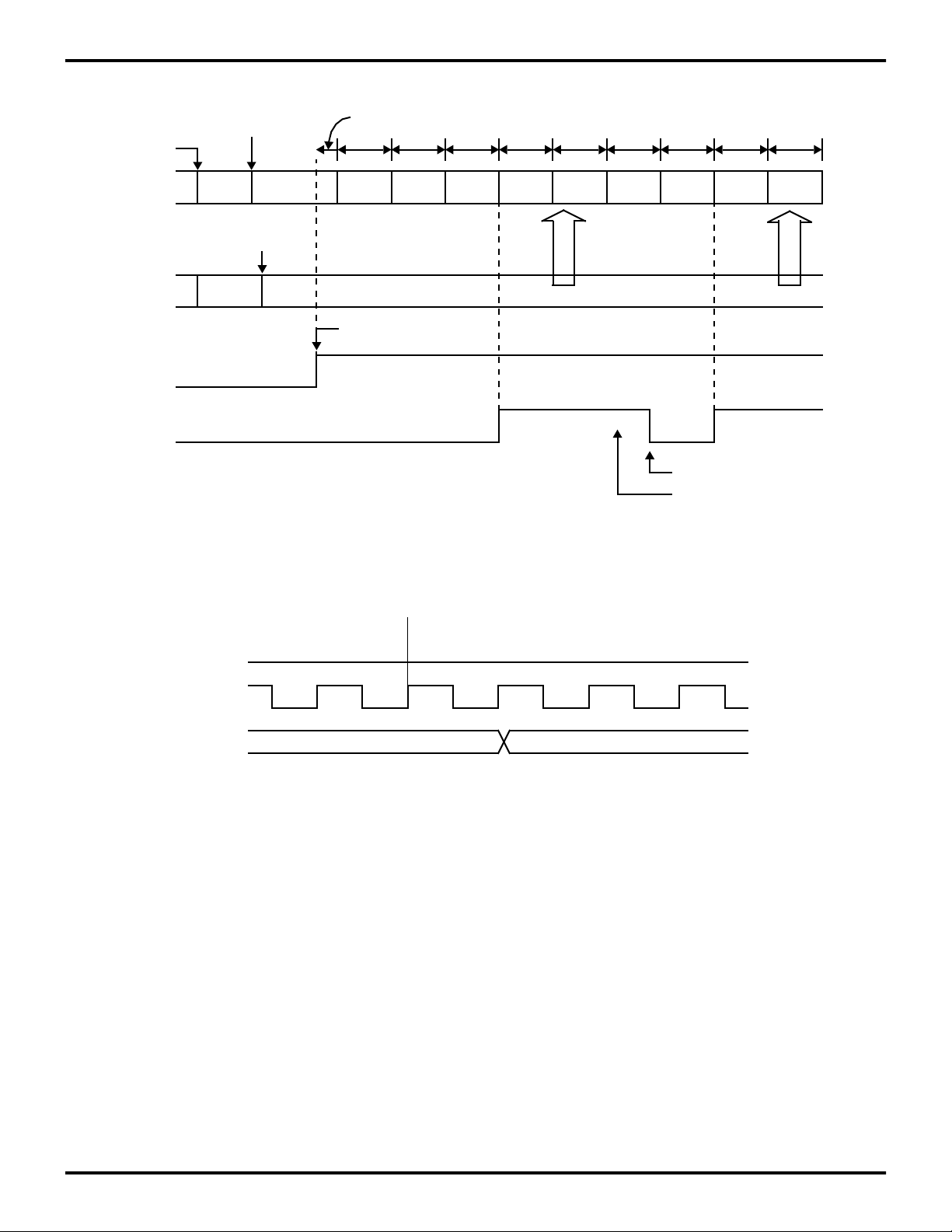
ARCHITECTURE
The Z180
®
combines a high-performance CPU core with a
variety of system and I/O resources useful in a broad
range of applications. The CPU core consists of five func-
tional blocks: clock generator, bus state controller, Inter-
rupt controller, memory management unit (MMU), and the
central processing unit (CPU). The integrated I/O resourc-
es make up the remaining four function blocks: direct
memory access (DMA) control (2 channels), asynchro-
nous serial communication interface (ASCI, 2 channels)
programmable reload timers (PRT, 2 channels), and a
clock serial I/O (CSIO) channel.
Clock Generator. Generates system clock from an exter-
nal crystal or clock input. The external clock is divided by
two or one and provided to both internal and external de-
vices.
Bus State Controller. This logic performs all of the status
and bus control activity associated with both the CPU and
some on-chip peripherals. This includes wait-state timing,
reset cycles, DRAM refresh, and DMA bus exchanges.
Interrupt Controller. This logic monitors and prioritizes
the variety of internal and external interrupts and traps to
provide the correct responses from the CPU. To maintain
compatibility with the Z80
®
CPU, three different interrupts
modes are supported.
Memory Management Unit. The MMU allows the user to
“map” the memory used by the CPU (logically only 64KB)
into the 1 MB addressing range supported by the
Z80180/Z8S180/Z8L180. The organization of the MMU
object code maintains compatibility with the Z80 CPU,
while offering access to an extended memory space. This
is accomplished by using an effective “common area-
banked area” scheme.
Central Processing Unit. The CPU is microcoded to pro-
vide a core that is object-code compatible with the Z80
CPU. It also provides a superset of the Z80 instruction set,
including 8-bit multiply. The core has been modified to al-
low many of the instructions to execute in fewer clock cy-
cles.
DMA Controller. The DMA controller provides high speed
transfers between memory and I/O devices. Transfer op-
erations supported are memory-to-memory, memory
to/from I/O, and I/O-to-I/O. Transfer modes supported are
request, burst, and cycle steal. DMA transfers can access
the full 1 MB address range with a block length up to 64
KB, and can cross over 64K boundaries.
Asynchronous Serial Communication Interface (AS-
CI). The ASCI logic provides two individual full-duplex
UARTs. Each channel includes a programmable baud rate
generator and modem control signals. The ASCI channels
can also support a multiprocessor communication format
as well as break detection and generation.
Programmable Reload Timers (PRT). This logic consists
of two separate channels, each containing a 16-bit counter
(timer) and count reload register. The time base for the
counters is derived from the system clock (divided by 20)
before reaching the counter. PRT channel 1 provides an
optional output to allow for waveform generation.
Z80180/Z8S180/Z8L180
Zilog Enhanced Z180 Microprocessor
DS971800401 P R E L I M I N A R Y 1-13
1
Figure 5. Timer Initialization, Count Down, and Reload Timing
FFFFH 0004H 0003H
0002H 0001H 0000H 0003H 0002H
0001H
0000H 0003H
Timer Data Register
Write (0004H)
Timer Data
Register
Timer Reload
Register
TDE Flag
TIF Flag
Reset
20 φ 20 φ 20 φ 20 φ 20 φ 20 φ 20 φ 20 φ 20 φ
0 < t < 20 φ
Timer Reload Register Write (0003H)
FFFFH
0003H
Reload
Reload
Write “1” to TDE
Timer Data Register Read
Timer Control Requestor Read
Figure 6. Timer Output Timing
Timer Data
Reg. = 0001H
Timer Data
Reg. = 0000H
TOUT
φ
Z80180/Z8S180/Z8L180
Enhanced Z180 Microprocessor Zilog
1-14 P R E L I M I N A R Y DS971800401
Clocked Serial I/O (CSI/O). The CSIO channel provides a
half-duplex serial transmitter and receiver. This channel
can be used for simple high-speed data connection to an-
other microprocessor or microcomputer. TRDR is used for
both CSI/O transmission and reception. Thus, the system
design must ensure that the constraints of half-duplex op-
eration are met (Transmit and Receive operation cannot
occur simultaneously). For example, if a CSI/O transmis-
sion is attempted while the CSI/O is receiving data, a
CSI/O will not work. Also note that TRDR is not buffered.
Therefore, attempting to perform a CSI/O transmit while
the previous transmit data is still being shifted out causes
the shift data to be immediately updated, thereby corrupt-
ing the transmit operation in progress. Similarly, reading
TRDR while a transmit or receive is in progress should be
avoided.
OPERATION MODES
Z80
®
versus 64180 Compatibility. The
Z80180/Z8S180/Z8L180 is descended from two different
“ancestor” processors, Zilog's original Z80 and the Hitachi
64180. The Operating Mode Control Register (OMCR),
shown in Figure 8, can be programmed to select between
certain Z80 and 64180differences.
M1E (M1 Enable). This bit controls the M1 output and is
set to a 1 during reset.
When M1E=1, the M1 output is asserted Low during the
opcode fetch cycle, the INT0 acknowledge cycle, and the
first machine cycle of the NMI acknowledge.
On the Z80180/Z8S180/Z8L180, this choice makes the
processor fetch an RETI instruction once, and when fetch-
ing an RETI from zero-wait-state memory will use three
clock machine cycles, which are not fully Z80-timing com-
patible but are compatible with the on-chip CTCs.
When M1E=0, the processor does not drive M1 Low during
instruction fetch cycles, and after fetching an RETI instruc-
tion once with normal timing, it goes back and re-fetches
the instruction using fully Z80-compatible cycles that in-
clude driving M1 Low. This may be needed by some exter-
nal Z80 peripherals to properly decode the RETI instruc-
tion. Figure 9 and Table 4 show the RETI sequence when
M1E=0.
Figure 7. CSIO Block Diagram
Internal Address/Data Bus
CSI/O T r ansmit/Receive
Data Register:
TRDR (8)
CSI/O Control Register:
CNTR (8)
Baud Rate
Generator
TXS
RXS
CKS
φ
Interrupt Request
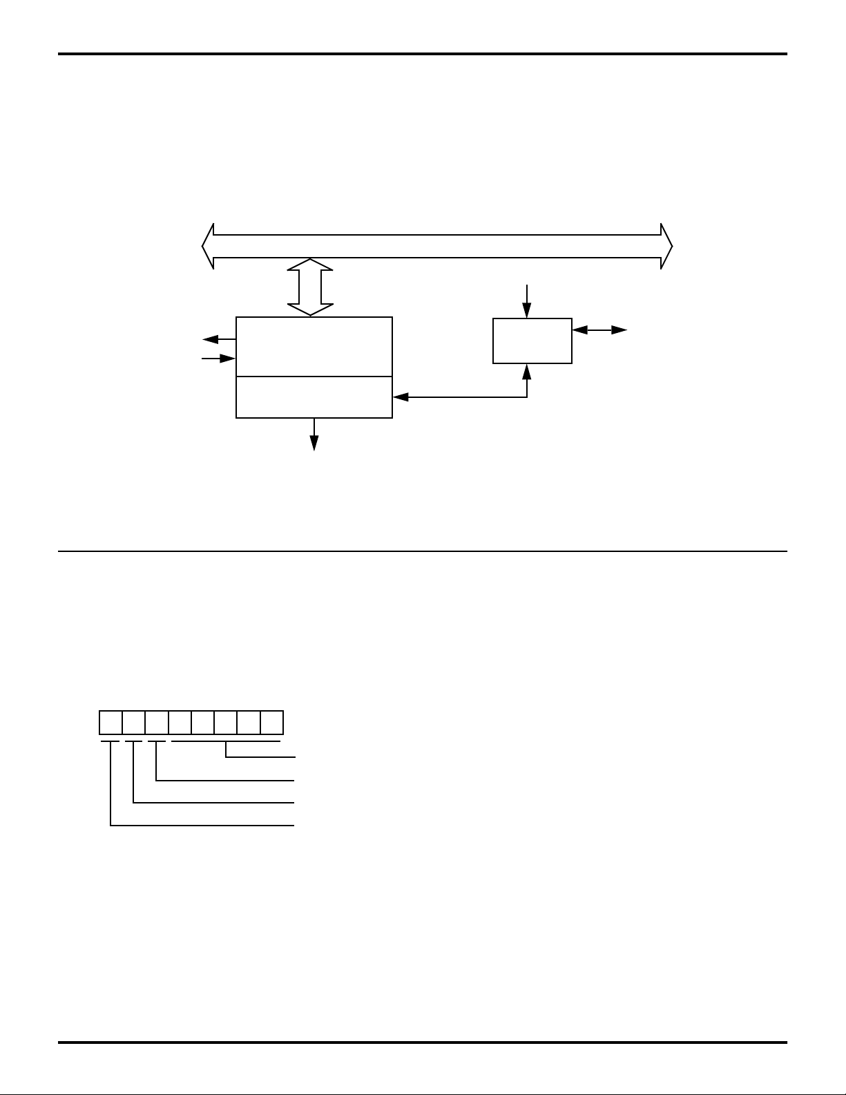
Figure 8. Operating Control Register
(OMCR: I/O Address = 3EH)
D7
Reserved
D6 D5
--
M1E (R/W)
--
-- --
--
/IOC (R/W)
/M1TE (W)
Z80180/Z8S180/Z8L180
Zilog Enhanced Z180 Microprocessor
DS971800401 P R E L I M I N A R Y 1-15
1
M1TE (M1 Temporary Enable). This bit controls the tem-
porary assertion of the /M1 signal. It is always read back
as a 1 and is set to 1 during reset.
When M1E is set to 0 to accommodate certain external
Z80 peripheral(s), those same device(s) may require a
pulse on M1 after programming certain of their registers to
complete the function being programmed.
For example, when a control word is written to the Z80 PIO
to enable interrupts, no enable actually takes place until
the PIO sees an active M1 signal. When M1TE=1, there is
no change in the operation of the /M1 signal and M1E con-
trols its function. When M1TE=0, the M1 output will be as-
serted during the next opcode fetch cycle regardless of the
state programmed into the M1E bit. This is only momen-
tary (one time) and the user need not preprogram a 1 to
disable the function (see Figure10).
Figure 9. RETI Instruction Sequence with MIE=0
T
1
T
2
T
3
T
1
T
2
T
3
T
I
T
I
T
I
T
1
T
2
T
3
T
1
T
2
T
3
T
I
T
I
A
0
-A
18
(A
19
)
φ
D
0
-D
7
PC
PC+1
PC PC+1
EDH
4DH EDH
4DH
MREQ
M1
RD
ST
Table 4. RETI Control Signal States with MIE=0
Machine M1
Cycle States Address Data RD WR MREQ IORQ IOC=1 IOC=0 HALT ST
1 T1-T3 1st Opcode EDH 0 1 0 1 0 1 1 0
2 T1-T3 2nd Opcode 4DH 0 1 0 1 0 1 1 0
Ti NA Tri-State 1 1 1 1 1 1 1 1
Ti NA Tri-State 1 1 1 1 1 1 1 1
Ti NA Tri-State 1 1 1 1 1 1 1 1
3 T1-T3 1st Opcode EDH 0 1 0 1 0 0 1 1
Ti NA Tri-State 1 1 1 1 1 1 1 1
4 T1-T3 2nd Opcode 4DH 0 1 0 1 0 1 1 1
5 T1-T3 SP Data 0 1 0 1 1 1 1 1
6 T1-T3 SP+1 Data 0 1 0 1 1 1 1 1
Z80180/Z8S180/Z8L180
Enhanced Z180 Microprocessor Zilog
1-16 P R E L I M I N A R Y DS971800401
IOC. This bit controls the timing of the /IORQ and /RD sig-
nals. It is set to 1 by reset.
When /IOC=1, the /IORQ and /RD signals function the
same as the Z64180 (Figure 11).
When /IOC = 0, the timing of the /IORQ and RD
signals
match the timing of the Z80. The /IORQ and /RD signals
go active as a result of the rising edge of T2. (Figure 12.)
Figure 10. M1 Temporary Enable Timing
T
1
T
2
T
3
T
1
T
2
T
3
φ
/WR
/M1
Opcode Fetch
Write into OMCR
Figure 11. I/O Read and Write Cycles with IOC = 1
T
1
T
2
T
W
T
3
φ
/IORQ
/RD
/WR
Figure 12. I/O Read and Write Cycles with IOC = 0
T
1
T
2
T
W
T
3
φ
/IORQ
/RD
/WR
Z80180/Z8S180/Z8L180
Zilog Enhanced Z180 Microprocessor
DS971800401 P R E L I M I N A R Y 1-17
1
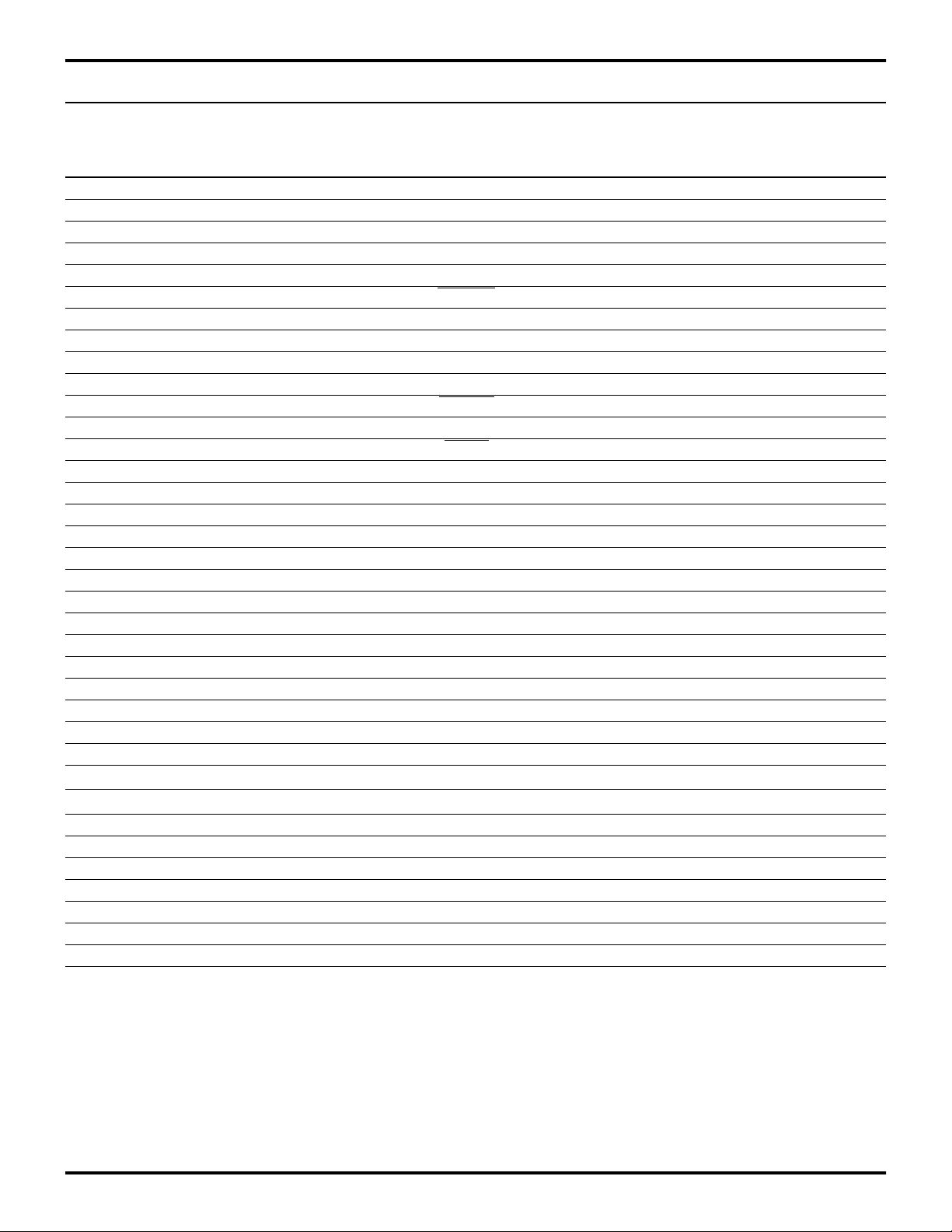
HALT and Low-Power Operating Modes. The
Z80180/Z8S180/Z8L180 can operate in seven modes with
respect to activity and power consumption:
– Normal Operation
– HALT Mode
– IOSTOP Mode
– SLEEP Mode
– SYSTEM STOP Mode
– IDLE Mode
– STANDBY Mode (with or without QUICK
RECOVERY)
Normal Operation. The Z80180/Z8S180/Z8L180 proces-
sor is fetching and running a program. All enabled func-
tions and portions of the device are active, and the HALT
pin is High.
HALT Mode. This mode is entered by the HALT instruc-
tion. Thereafter, the Z80180/Z8S180/Z8L180 processor
continually fetches the following opcode but does not exe-
cute it, and drives the HALT, ST and M1 pins all Low. The
oscillator and PHI pin remain active, interrupts and bus
granting to external masters, and DRAM refresh can occur
and all on-chip I/O devices continue to operate including
the DMA channels.
The Z80180/Z8S180/Z8L180 leaves HALT mode in re-
sponse to a Low on RESET, on to an interrupt from an en-
abled on-chip source, an external request on NMI, or an
enabled external request on INT0, INT1, or INT2. In case
of an interrupt, the return address will be the instruction fol-
lowing the HALT instruction; at that point the program can
either branch back to the HALT instruction to wait for an-
other interrupt, or can examine the new state of the sys-
tem/application and respond appropriately.
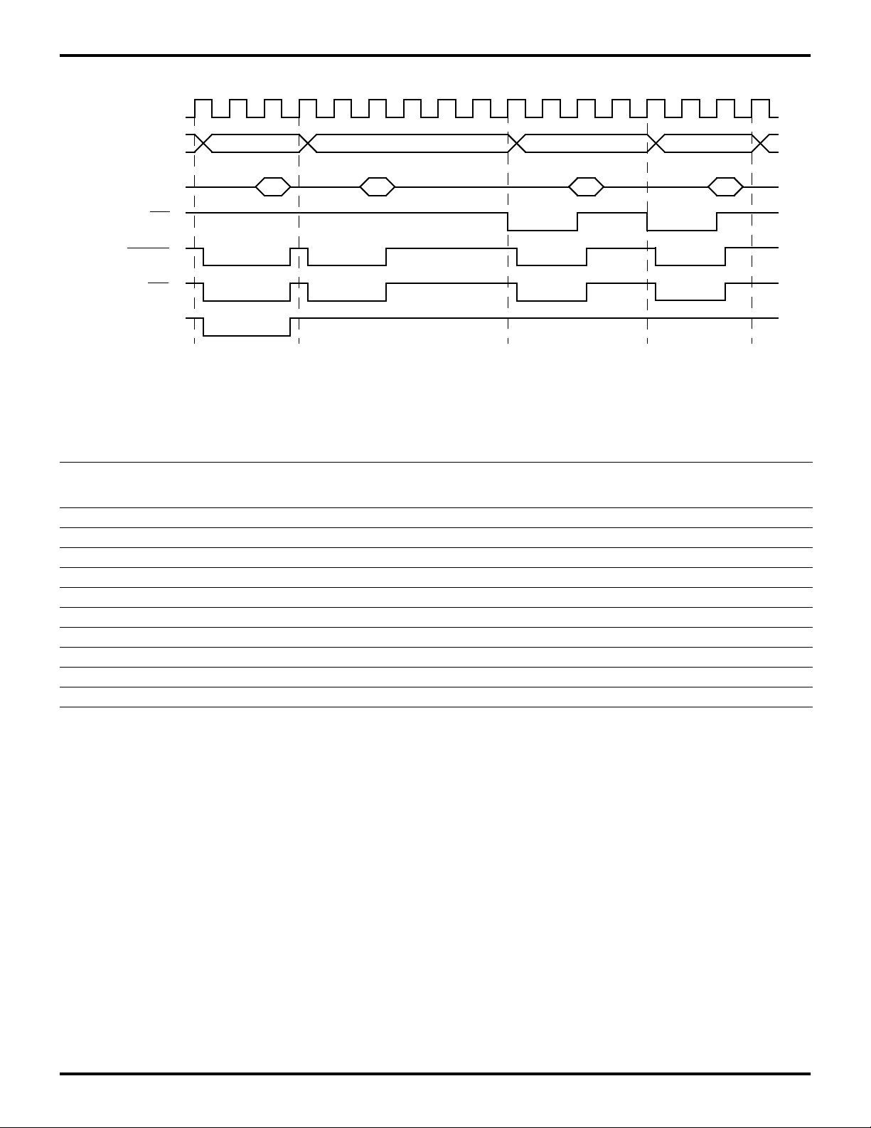
SLEEP Mode. This mode is entered by keeping the
IOSTOP bit (ICR5) bits 3 and 6 of the CPU Control Regis-
ter (CCR3, CCR6) all zero and executing the SLP instruc-
tion. The oscillator and PHI output continue operating, but
are blocked from the CPU core and DMA channels to re-
duce power consumption. DRAM refresh stops but inter-
rupts and granting to external master can occur. Except
when the bus is granted to an external master, A19-0 and
all control signals except /HALT are maintained High.
/HALT is Low. I/O operations continue as before the SLP
instruction, except for the DMA channels.
The Z80180/Z8S180/Z8L180 leaves SLEEP mode in re-
sponse to a low on /RESET, an interrupt request from an
on-chip source, an external request on /NMI, or an external
request on /INT0, 1, or 2.
Figure 13. HALT Timing
INT
i
, NMI
A
0
-A
19
/HALT
/M1
/MREQ
/RD
HALT Opcode Address
HALT Opcode Address + 1
Z80180/Z8S180/Z8L180
Enhanced Z180 Microprocessor Zilog
1-18 P R E L I M I N A R Y DS971800401
If an interrupt source is individually disabled, it cannot
bring the Z80180/Z8S180/Z8L180 out of SLEEP mode. If
an interrupt source is individually enabled, and the IEF bit
is 1 so that interrupts are globally enabled (by an EI in-
struction), the highest priority active interrupt will occur,
with the return address being the instruction after the SLP
instruction. If an interrupt source is individually enabled,
but the IEF bit is 0 so that interrupts are globally disabled
(by a DI instruction), the Z80180/Z8S180/Z8L180 leaves
SLEEP mode by simply executing the following instruc-
tion(s).
This provides a technique for synchronization with high-
speed external events without incurring the latency im-
posed by an interrupt response sequence. Figure 14
shows the timing for exiting SLEEP mode due to an inter-
rupt request. Note that the Z80180/Z8S180/Z8L180 takes
about 1.5 clocks to restart.
IOSTOP Mode. IOSTOP mode is entered by setting the
IOSTOP bit of the I/O Control Register (ICR) to 1. In this
case, on-chip I/O (ASCI, CSI/O, PRT) stops operating.
However, the CPU continues to operate. Recovery from
IOSTOP mode is by resetting the IOSTOP bit in ICR to 0.
SYSTEM STOP Mode. SYSTEM STOP mode is the com-
bination of SLEEP and IOSTOP modes. SYSTEM STOP
mode is entered by setting the IOSTOP bit in ICR to 1 fol-
lowed by execution of the SLP instruction. In this mode,
on-chip I/O and CPU stop operating, reducing power con-
sumption, but the PHI output continues to operate. Recov-
ery from SYSTEM STOP mode is the same as recovery
from SLEEP mode except that internal I/O sources (dis-
abled by IOSTOP) cannot generate a recovery interrupt.
IDLE Mode. Software can put the
Z80180/Z8S180/Z8L180 into this mode by setting the
IOSTOP bit (ICR5) to 1, CCR6 to 0, CCR3 to 1 and exe-
cuting the SLP instruction. The oscillator keeps operating
but its output is blocked to all circuitry including the PHI
pin. DRAM refresh and all internal devices stop, but exter-
nal interrupts can occur. Bus granting to external masters
can occur if the BREST bit in the CPU control Register
(CCR5) was set to 1 before IDLE mode was entered.
The Z80180/Z8S180/Z8L180 leaves IDLE mode in re-
sponse to a Low on RESET, an external interrupt request
on NMI, or an external interrupt request on /INT0, /INT1 or
/INT2 that is enabled in the INT/TRAP Control Register. As
previously described for SLEEP mode, when the
Z80180/Z8S180/Z8L180 leaves IDLE mode due to an
NMI, or due to an enabled external interrupt request when
the IEF flag is 1 due to an EI instruction, it starts by per-
forming the interrupt with the return address being that of
the instruction after the SLP instruction.
If an external interrupt enables the INT/TRAP control reg-
ister while the IEF1 bit is 0, Z80180/Z8S180/Z8L180
leaves IDLE mode; specifically, the processor restarts by
executing the instructions following the SLP instruction.
Figure 14. SLEEP Timing
SLP 2nd Opcode
SLEEP Mode
φ
T
2
T
3
T
1
T
2
T
S
T
S
T
1
/INTi, /NMI
A
0
-A
19
/HALT
M1
Opcode Fetch or Interrupt
Acknowledge Cycle
SLP 2nd Opcode Address
FFFFFH
Fetch Cycle
T
2
T
3
Z80180/Z8S180/Z8L180
Zilog Enhanced Z180 Microprocessor
DS971800401 P R E L I M I N A R Y 1-19
1
Figure 15 shows the timing for exiting IDLE mode due to
an interrupt request. Note that the
Z80180/Z8S180/Z8L180 takes about 9.5 clocks to restart.
While the Z80180/Z8S180/Z8L180 is in IDLE mode, it will
grant the bus to an external master if the BREXT bit
(CCR5) is 1. Figure 16 shows the timing for this sequence.
Note that the part takes 8 clock cycles longer to respond to
the Bus Request than in normal operation.
After the external master negates the Bus Request, the
Z80180/Z8S180/Z8L180 disables the PHI clock and re-
mains in IDLE mode.
Figure 15. Z80180/Z8S180/Z8L180 IDLE Mode Exit due to External Interrupt
φ
T
1
T
2
T
4
NMI
A
19
-A
0
HALT
M1
Opcode Fetch or Interrupt
Acknowledge Cycle
FFFFFH
IDLE Mode
T
3
9.5 Cycle Delay from INTi Asserted
INTi
or
Z80180/Z8S180/Z8L180
Enhanced Z180 Microprocessor Zilog
1-20 P R E L I M I N A R Y DS971800401
STANDBY Mode (With or Without QUICK RECOVERY).
Software can put the Z80180/Z8S180/Z8L180 into this
mode by setting the IOSTOP bit (ICR5) to 1 and CCR6 to
1, and executing the SLP instruction. This mode stops the
on-chip oscillator and thus draws the least power of any
mode, less than 10µµA.
As with IDLE mode, the Z80180/Z8S180/Z8L180 will leave
STANDBY mode in response to a Low on RESET
or on
NMI
, or a Low on INT0-2 that is enabled by a 1 in the cor-
responding bit in the INT/TRAP Control Register, and will
grant the bus to an external master if the BREXT bit in the
CPU Control Register (CCR5) is 1. But the time required
for all of these operations is greatly increased by the need
to restart the on-chip oscillator and ensure that it has sta-
bilized to square-wave operation.
When an external clock is connected to the EXTAL pin
rather than a crystal to the XTAL and EXTAL pins, and the
external clock runs continuously, there is little need to use
STANDBY mode because there is no time required to re-
start the oscillator, and other modes restart faster. Howev-
er, if external logic stops the clock during STANDBY mode
(for example, by decoding HALT Low and M1 High for sev-
eral clock cycles), then STANDBY mode can be useful to
allow the external clock source to stabilize after it is re-en-
abled.
When external logic drives RESET Low to being a
Z80180/Z8S180/Z8L180 out of STANDBY mode, and a
crystal is used or an external clock source has been
stopped, the external logic must hold RESET
Low until the
on-chip oscillator or external clock source has restarted
and stabilized.
The clock stability requirements of the
Z80180/Z8S180/Z8L180 are much less in the divide-by-
two mode that's selected by a Reset sequence and there-
after controlled by the Clock Divide bit in the CPU Control
Register (CCR7). Because of this, software should:
a. Program CCR7 to 0 to select divide-by-two mode,
before the SLP instruction that enters STANDBY
mode, and.
b. After a Reset, interrupt or in-line restart after the
SLP 01 instruction, delay programming CCR7
back to 1 to set divide-by-one mode, as long as
possible to allow additional clock stabilization
time.
If software sets CCR6 to 1 before the SLP instruction plac-
es the MPU in STANDBY mode, the value in the CCR3 bit
determines how long the Z80180/Z8S180/Z8L180 will wait
for oscillator restart and stabilization when it leaves
STANDBY mode due to an external interrupt request. If
CCR3 is 0, the Z80180/Z8S180/Z8L180 waits 217
(131,072) clock cycles, while if CCR3 is 1, it waits only 64
clock cycles. The latter is called QUICK RECOVERY
mode. The same delay applies to granting the bus to an
Figure 16. Bus Granting to External Master in IDLE Mode
φ
TX
BUSREQ
A
19
-A
0
HALT
M1
Bus RELEASE Mode
IDLE Mode
FFFFFH
IDLE Mode
9.5 Cycle Delay until BUSACK Asserted
BUSACK
TX
High Impedance
FFFFFH
High
Low
Z80180/Z8S180/Z8L180
Zilog Enhanced Z180 Microprocessor
DS971800401 P R E L I M I N A R Y 1-21
1
external master during STANDBY mode, when the BREXT
bit in the CPU Control Register (CCR5) is 1.
As described previously for SLEEP and IDLE modes,
when a Z80180/Z8S180/Z8L180 leaves STANDBY mode
due to NMI Low, or when it leaves STANDBY mode due to
an enabled INTO-2 low when the IEF, flag is 1 due to an
IE instruction, it starts by performing the interrupt with the
return address being that of the instruction following the
SLP instruction. If the Z80180/Z8S180/Z8L180 leaves
STANDBY mode due to an external interrupt request that's
enabled in the INT/TRAP Control Register, but the IEF, bit
is 0 due to a DI instruction, the processor restarts by exe-
cuting the instruction(s) following the SLP instruction. If
INT0, or INT1 or 2 goes inactive before the end of the clock
stabilization delay, the Z80180/Z8S180/Z8L180 stays in
STANDBY mode.
Figure 17 shows the timing for leaving STANDBY mode
due to an interrupt request. Note that the
Z80180/Z8S180/Z8L180 takes either 64 or 217 (131,072)
clocks to restart, depending on the CCR3 bit.
While the Z80180/Z8S180/Z8L180 is in STANDBY mode,
it will grant the bus to an external master if the BREXT bit
(CCR5) is 1. Figure 18 shows the timing of this sequence.
Note that the part takes 64 or 217 (131,072) clock cycles
to grant the bus depending on the CCR3 bit.
The latter (non-Quick-Recovery) case may be prohibitive
for many “demand driven” external masters. If so, QUICK
RECOVERY or IDLE mode can be used.
Figure 17. Z80180/Z8S180/Z8L180 STANDBY Mode Exit due to External Interrupt
φ
T
1
T
2
T
4
NMI
A
19
-A
0
HALT
M1
Opcode Fetch or Interrupt
Acknowledge Cycle
FFFFFH
STANDBY Mode
T
3
2
17
or 64 Cycle Delay from INTi Asserted
INTi
or
 Loading...