


 Loading...
ZILOG Z86E3016SSC, Z86E3016VEC, Z86E3016VSC, Z86E3116KEE, Z86E3116KSE Datasheet
...PRELIMINARY PRODUCT SPECIFICATION
1
Z86E30/E31/E40 1
Z8 4K OTP MICROCONTROLLER
FEATURES
|
ROM |
RAM* |
I/O |
Speed |
Device |
(KB) |
(Bytes) |
Lines |
(MHz) |
|
|
|
|
|
Z86E30 |
4 |
237 |
24 |
16 |
Z86E31 |
2 |
125 |
24 |
16 |
Z86E40 |
4 |
236 |
32 |
16 |
|
|
|
|
|
Note: *General-Purpose
■Standard Temperature (VCC = 3.5V to 5.5V)
■Extended Temperature (VCC = 4.5V to 5.5V)
■Available Packages:
28-Pin DIP/SOIC/PLCC OTP (Z86E30/31 only)
28-Pin DIP Window (Z86E30/31 only)
40-Pin DIP OTP/Window (Z86E40 only)
44-Pin PLCC/QFP OTP (Z86E40 only)
44-Pin PLCC Window (Z86E40 only)
■Software Enabled Watch-Dog Timer (WDT)
■Push-Pull/Open-Drain Programmable on Port 0, Port 1, and Port 2
■24/32 Input/Output Lines
■Auto Latches
■Auto Power-On Reset (POR)
■Programmable OTP Options: RC Oscillator
EPROM Protect Auto Latch Disable
Permanently Enabled WDT
Crystal Oscillator Feedback Resistor Disable RAM Protect
■Low-Power Consumption: 60 mW
■Fast Instruction Pointer: 0.75 s
■Two Standby Modes: STOP and HALT
■Digital Inputs CMOS Levels, Schmitt-Triggered
■Software Programmable Low EMI Mode
■Two Programmable 8-Bit Counter/Timers Each with a 6-Bit Programmable Prescaler
■Six Vectored, Priority Interrupts from Six Different Sources
■Two Comparators
■On-Chip Oscillator that Accepts a Crystal, Ceramic Resonator, LC, RC, or External Clock Drive
GENERAL DESCRIPTION
The Z86E30/E31/E40 8-Bit One-Time Programmable (OTP) Microcontrollers are members of Zilog's single-chip Z8® MCU family featuring enhanced wake-up circuitry, programmable Watch-Dog Timers, Low Noise EMI options, and easy hardware/software system expansion capability.
Four basic address spaces support a wide range of memory configurations. The designer has access to three addi-
tional control registers that allow easy access to register mapped peripheral and I/O circuits.
For applications demanding powerful I/O capabilities, the Z86E30/E31 have 24 pins, and the Z86E40 has 32 pins of dedicated input and output. These lines are grouped into four ports, eight lines per port, and are configurable under software control to provide timing, status signals, and par-
DS97Z8X0500 |
P R E L I M I N A R Y |
1 |
Z86E30/E31/E40 |
|
Z8 4K OTP Microcontroller |
Zilog |
allel I/O with or without handshake, and address/data bus for interfacing external memory.
Notes: All Signals with a preceding front slash, "/", are active Low, for example, B//W (WORD is active Low); /B/W (BYTE is active Low, only).
Power connections follow conventional descriptions below:
Connection |
Circuit |
Device |
|
|
|
Power |
VCC |
VDD |
Ground |
GND |
VSS |
|
|
|
|
(E40 Only) |
||
|
VCC |
|
|
|
|
|
|
|
|
|
|
|
|
|
|
|
|
|
|
|
Output Input |
GND |
XTAL /AS /DS R//W /RESET |
||||
|
|
|
|
|
|
|
|
|
|
|
|
|
|
|
|
|
|
|
|
|
|
|
|
|
|
|
|
|
|
|
|
|
|
|
|
|
|
|
|
|
|
|
|
|
|
|
|
|
|
|
|
|
|
|
|
|
|
|
|
|
|
|
|
|
|
|
|
|
|
|
|
|
|
|
|
|
|
|
|
|
|
|
|
|
|
|
|
|
|
|
|
|
|
|
|
|
|
|
|
|
|
|
|
|
|
|
|
|
|
|
|
|
|
|
|
|
|
|
|
|
|
|
|
|
|
|
|
|
|
|
Port 3 |
|
|
|
|
|
|
|
|
|
|
|
|
|
|
|
|
|
|
|
|
|
|
Machine Timing |
|||||||||||||||||
|
|
|
|
|
|
|
|
|
|
|
|
|
|
|
|
|
|
|
|
|
|
|
|
|||||||||||||||||||
|
|
|
|
|
|
|
|
|
|
|
|
|
|
|
|
|
|
|
|
|
||||||||||||||||||||||
|
|
|
|
|
|
|
|
|
|
|
|
|
|
|
|
|
|
|
|
|
& |
|
|
|
|
|||||||||||||||||
|
|
|
|
|
|
|
|
|
|
|
|
|
|
|
|
|
|
|
|
|
|
|
|
|
|
|
|
|
|
|
|
|
|
|||||||||
|
|
|
|
|
|
|
|
|
|
|
|
|
|
|
|
|
|
|
|
|
|
|
|
|
|
|
|
|||||||||||||||
|
|
|
|
|
|
|
|
|
|
|
|
|
|
|
|
|
|
|
|
|
|
|
|
|
|
|
|
|
|
|
|
|
Instruction Control |
|||||||||
|
|
|
|
|
|
|
|
|
|
|
|
|
|
|
|
|
|
|
|
|
|
|
|
|
|
|
|
|
|
|||||||||||||
|
|
|
|
|
|
|
|
|
|
|
|
|
|
|
|
|
|
|
|
|
|
|
|
|
|
|
|
|
|
|
|
|
|
|
|
|
|
|
|
|
|
|
|
|
Counter/ |
|
|
|
|
|
ALU |
|
|
|
|
|
|
|
|
|
|
|
|
RESET |
|||||||||||||||||||||
|
|
|
|
|
|
|
|
|
|
|
|
|||||||||||||||||||||||||||||||
|
|
|
|
|
|
|
|
|
|
|
|
|
|
|
|
|
|
WDT, POR |
||||||||||||||||||||||||
|
|
Timers (2) |
|
|
|
|
|
|
|
|
|
|
|
|
|
|
|
|
||||||||||||||||||||||||
|
|
|
|
|
|
|
|
|
|
|
|
|
|
|
|
FLAGS |
|
|
|
|
|
|
|
|
|
|
|
|
|
|
|
|
|
|
|
|
|
|||||
|
|
|
|
|
|
|
|
|
|
|
|
|
|
|
|
|
|
|
|
|
|
|
|
|
|
|
|
|
|
|
|
|
|
|
|
|
||||||
|
|
Interrupt |
|
|
|
|
|
|
|
|
|
|
|
|
|
|
|
|
|
|
|
|
|
|
|
OTP |
|
|
||||||||||||||
|
|
|
|
|
|
|
|
|
|
|
|
|
|
|
|
|
|
|
|
|
|
|
|
|
||||||||||||||||||
|
|
Control |
|
|
|
|
|
|
|
|
|
|
|
|
|
|
|
|
|
|
|
|
|
|
|
|
|
|||||||||||||||
|
|
|
|
|
|
|
|
|
|
|
|
|
|
|
|
|||||||||||||||||||||||||||
|
|
|
|
|
|
|
|
|
|
|
|
|
|
|
|
|||||||||||||||||||||||||||
|
|
|
|
|
|
|
|
|
|
|
|
|
|
|
|
|
|
|
|
|
|
|
|
|
|
|
|
|
|
|
|
|
|
|
|
|
|
|
||||
|
|
|
|
|
|
|
|
|
|
|
|
|
|
|
|
Register |
|
|
|
|
|
|
|
|
|
|
|
|
|
|
|
|
|
|
|
|
|
|||||
|
|
|
|
|
|
|
|
|
|
|
|
|
|
|
|
|
|
|
|
|
|
|
|
|
|
|
|
|
|
|
|
|
|
|
|
|
||||||
|
Two Analog |
|
|
|
|
|
Pointer |
|
|
|
|
|
|
|
|
|
|
|
|
|
|
|
|
|
|
|
|
|
||||||||||||||
|
|
|
|
|
|
|
|
|
|
|
|
|
|
|
|
|
|
|
||||||||||||||||||||||||
|
Comparators |
|
|
|
|
Register File |
|
|
|
|
|
|
|
|
|
|
|
|
Program |
|
|
|||||||||||||||||||||
|
|
|
|
|
|
|
|
|
|
|
|
|
|
|
|
|
||||||||||||||||||||||||||
|
|
|
|
|
|
|
|
|
|
|
|
|
|
|
|
|
|
|
|
|
|
|
|
|
|
|
Counter |
|
|
|||||||||||||
|
|
|
|
|
|
|
|
|
|
|
|
|
|
|
|
|
|
|
|
|
|
|
|
|
|
|
|
|
|
|
|
|
|
|
|
|
|
|
|
|
|
|
|
|
|
|
|
|
|
|
|
|
|
|
|
|
|
|
|
|
|
|
|
|
|
|
|
|
|
|
|
|
|
|
|
|
|
|
|
|
|
|
|
|
|
|
|
|
|
|
|
|
|
|
|
|
|
|
|
|
|
|
|
|
|
|
|
|
|
|
|
|
|
|
|
|
|
|
|
|
|
|
|
|
|
|
|
|
|
|
|
|
|
|
|
|
|
|
|
|
|
|
|
|
|
|
|
|
|
|
|
|
|
|
|
|
|
|
|
|
|
|
|
|
|
|
|
|
|
|
|
|
|
|
|
|
|
|
|
|
|
|
|
|
|
|
|
|
|
|
|
|
|
|
|
|
|
|
|
|
|
|
|
|
|
|
|
|
|
|
|
|
|
|
|
|
|
|
|
|
|
|
|
|
|
|
|
|
|
|
|
|
|
|
|
|
|
|
|
|
|
|
|
|
|
|
|
|
|
|
|
|
|
|
|
|
|
|
|
|
|
Port 2 |
|
|
|
|
|
Port 0 |
|
|
|
|
|
Port 1 |
|
||||||||||||||
|
|
|
|
|
|
|
|
|
|
|
|
|
|
|
|||||||||||||||||
|
|
|
|
|
|
|
|
|
|
|
|
|
|
|
|||||||||||||||||
|
|
|
|
|
|
|
|
|
|
|
|
|
|
|
|
|
|
|
|
|
|
|
|
|
|
|
|
|
|
|
|
|
|
|
|
|
|
|
|
|
|
|
|
|
|
|
|
|
|
|
|
|
|
|
|
|
|
|
|
|
|
|
|
|
|
|
|
|
|
|
|
|
|
|
|
|
|
4 |
|
|
|
4 |
|
|
|
|
|
|
|
|
|
8 |
|
|
|
|
|
|
|
|
|
|
|
|
|
|
|
|
|
|
|
|
|
|
|
|
|
|
|
||||||||
|
|
|
|
I/O |
|
|
|
|
|
|
|
|
|
|
|
|
|
|
|
|
|
|
|
|
|
||||||
|
|
|
|
|
Address or I/O |
|
Address/Data or I/O |
||||||||||||||||||||||||
(Bit Programmable) |
|
|
|||||||||||||||||||||||||||||
(Nibble Programmable) |
|
(Byte Programmable) |
|||||||||||||||||||||||||||||
|
|
|
|
|
|
|
|
|
|
|
|
||||||||||||||||||||
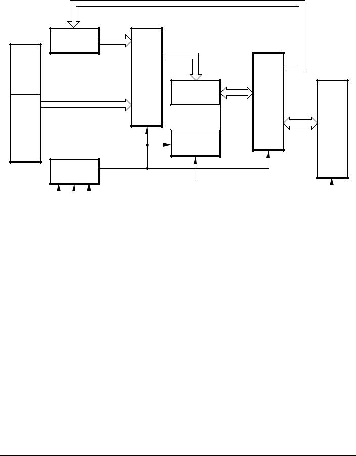
(E40 Only)
Figure 1. Z86E30/E31/E40 Functional Block Diagram
2 |
P R E L I M I N A R Y |
DS97Z8X0500 |
|
Z86E30/E31/E40 |
Zilog |
Z8 4K OTP Microcontroller |
|
|
|
D7 - 0 |
|
AD 11- 0 |
|
|
Z8 MCU |
AD 11- 0 |
|
|
|
|
|
|
MSN |
Address |
|
|
Port 3 |
MUX |
|
|
|
|
D7 - 0 |
|
|
EPROM |
Data |
|
AD 11- 0 |
MUX |
|
|
|
|
||
|
TEST ROM |
D7 - 0 |
Z8 |
Z8 |
|
|
Port 2 |
|
|
|
|
Port 0 |
OTP |
|
|
|
|
|
|
|
Options |
|
|
PGM + Test
Mode Logic
|
|
|
|
|
VPP |
|
|
|
|
|
|
P33 |
|
|
|
|
|
|
|
|
|
|
|
|
|
/OE |
|
EPM |
|
/PGM |
||||
|
P31 |
|||||
P32 |
|
P30 |
|
|
||
|
|
|
||||
/CE
XT1
Figure 2. EPROM Programming Block Diagram
DS97Z8X0500 |
P R E L I M I N A R Y |
3 |
Z86E30/E31/E40 |
|
Z8 4K OTP Microcontroller |
Zilog |
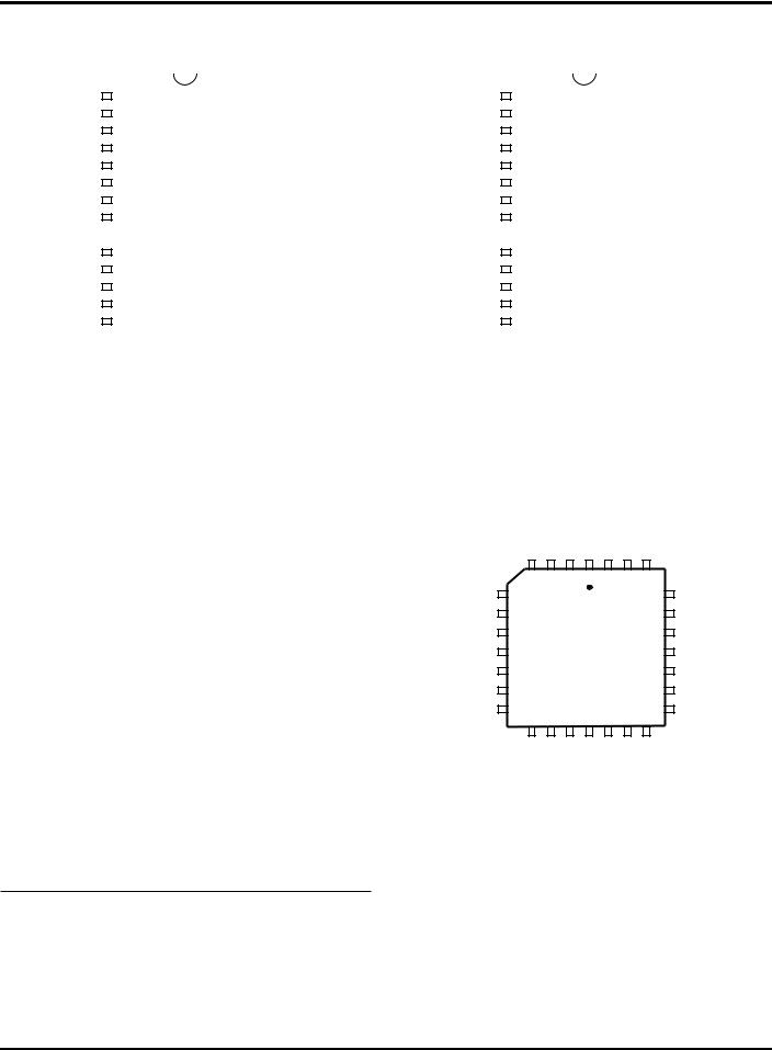
PIN IDENTIFICATION
R//W |
|
1 |
40 |
|
/DS |
|
|
||||||
|
||||||
P25 |
|
|
|
|
|
P24 |
|
|
|
|
|
||
|
|
|
|
|
||
P26 |
|
|
|
|
|
P23 |
|
|
|
|
|
||
|
|
|
|
|
||
P27 |
|
|
|
|
|
P22 |
|
|
|
|
|
||
|
|
|
|
|
||
P04 |
|
|
|
|
|
P21 |
|
|
|
|
|
||
|
|
|
|
|
||
P05 |
|
|
|
|
|
P20 |
|
|
|
|
|
||
|
|
|
|
|
||
P06 |
|
|
|
|
|
P03 |
|
|
|
|
|
||
|
|
|
|
|
||
P14 |
|
|
|
|
|
P13 |
|
|
|
|
|
||
|
|
|
|
|
||
P15 |
|
|
|
|
|
P12 |
|
|
|
|
|
||
|
|
|
|
|
||
P07 |
|
|
|
|
|
GND |
|
|
40-Pin DIP |
|
|||
|
|
|
||||
|
|
|
||||
VCC |
|
|
|
|
|
P02 |
|
|
|
|
|
||
|
|
|
|
|
||
P16 |
|
|
|
|
|
P11 |
|
|
|
|
|
||
|
|
|
|
|
||
P17 |
|
|
|
|
|
P10 |
|
|
|
|
|
||
|
|
|
|
|
||
XTAL2 |
|
|
|
|
|
P01 |
|
|
|
|
|
||
|
|
|
|
|
||
XTAL1 |
|
|
|
|
|
P00 |
|
|
|
|
|
||
|
|
|
|
|
||
P31 |
|
|
|
|
|
P30 |
|
|
|
|
|
||
|
|
|
|
|
||
P32 |
|
|
|
|
|
P36 |
|
|
|
|
|
||
|
|
|
|
|
||
P33 |
|
|
|
|
|
P37 |
|
|
|
|
|
||
|
|
|
|
|
||
P34 |
|
20 |
21 |
|
P35 |
|
|
|
|||||
|
|
|||||
/AS |
|
|
/RESET |
|||
|
||||||
|
||||||
|
|
|
|
|
|
|
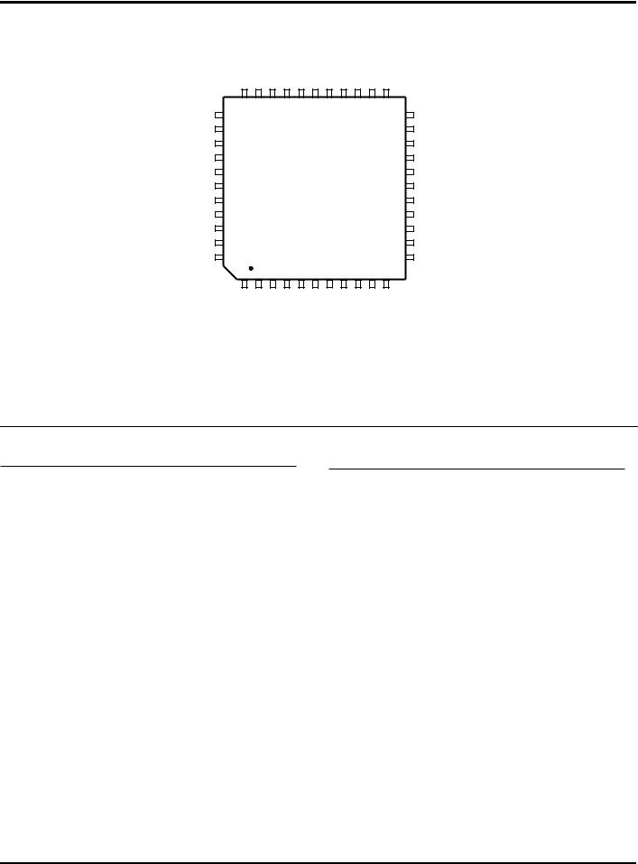
Figure 3. 40-Pin DIP Pin Configuration*
Standard Mode
Table 1. 40-Pin DIP Pin Identification
Standard Mode
Pin # |
Symbol |
Function |
Direction |
|
|
|
|
1 |
R//W |
Read/Write |
Output |
|
|
|
|
2-4 |
P25-P27 |
Port 2, Pins 5,6,7 |
In/Output |
|
|
|
|
5-7 |
P04-P06 |
Port 0, Pins 4,5,6 |
In/Output |
|
|
|
|
8-9 |
P14-P15 |
Port 1, Pins 4,5 |
In/Output |
|
|
|
|
10 |
P07 |
Port 0, Pin 7 |
In/Output |
|
|
|
|
11 |
VCC |
Power Supply |
|
12-13 |
P16-P17 |
Port 1, Pins 6,7 |
In/Output |
|
|
|
|
14 |
XTAL2 |
Crystal Oscillator |
Output |
|
|
|
|
15 |
XTAL1 |
Crystal Oscillator |
Input |
|
|
|
|
16-18 |
P31-P33 |
Port 3, Pins 1,2,3 |
Input |
|
|
|
|
19 |
P34 |
Port 3, Pin 4 |
Output |
|
|
|
|
20 |
/AS |
Address Strobe |
Output |
|
|
|
|
21 |
/RESET |
Reset |
Input |
|
|
|
|
22 |
P35 |
Port 3, Pin 5 |
Output |
|
|
|
|
23 |
P37 |
Port 3, Pin 7 |
Output |
|
|
|
|
24 |
P36 |
Port 3, Pin 6 |
Output |
|
|
|
|
25 |
P30 |
Port 3, Pin 0 |
Input |
|
|
|
|
26-27 |
P00-P01 |
Port 0, Pins 0,1 |
In/Output |
|
|
|
|
28-29 |
P10-P11 |
Port 1, Pins 0,1 |
In/Output |
|
|
|
|
30 |
P02 |
Port 0, Pin 2 |
In/Output |
|
|
|
|
31 |
GND |
Ground |
|
|
|
|
|
32-33 |
P12-P13 |
Port 1, Pins 2,3 |
In/Output |
|
|
|
|
34 |
P03 |
Port 0, Pin 3 |
In/Output |
|
|
|
|
35-39 |
P20-P24 |
Port 2, Pins |
In/Output |
|
|
0,1,2,3,4 |
|
|
|
|
|
40 |
/DS |
Data Strobe |
Output |
|
|
|
|
Notes:
*Pin Configuration and Identification identical on DIP and Cerdip Window Lid style packages.
4 |
P R E L I M I N A R Y |
DS97Z8X0500 |
|
Z86E30/E31/E40 |
Zilog |
Z8 4K OTP Microcontroller |
|
|
|
P20 |
P03 |
P13 |
P12 |
GND |
GND |
P02 |
P11 |
P10 |
P01 |
P00 |
|
|
6 |
|
|
|
|
1 |
|
|
|
|
40 |
|
P21 |
7 |
|
|
|
|
|
|
|
|
|
39 |
P30 |
P22 |
|
|
|
|
|
|
|
|
|
|
|
P36 |
P23 |
|
|
|
|
|
|
|
|
|
|
|
P37 |
P24 |
|
|
|
|
|
|
|
|
|
|
|
P35 |
/DS |
|
|
|
44-Pin PLCC |
|
|
|
/RESET |
||||
NC |
|
|
|
|
|
|
R//RL |
|||||
R//W |
|
|
|
|
|
|
|
|
|
|
|
/AS |
P25 |
|
|
|
|
|
|
|
|
|
|
|
P34 |
P26 |
|
|
|
|
|
|
|
|
|
|
|
P33 |
P27 |
|
|
|
|
|
|
|
|
|
|
|
P32 |
P04 |
17 |
|
|
|
|
|
|
|
|
|
29 |
P31 |
|
18 |
|
|
|
|
|
|
|
|
|
28 |
|
|
P05 |
P06 |
P14 |
P15 |
P07 |
VCC |
VCC |
P16 |
P17 |
XTAL2 |
XTAL1 |
|
Figure 4. 44-Pin PLCC Pin Configuration
Standard Mode
Table 2. 44-Pin PLCC Pin Identification
Pin # |
Symbol |
Function |
Direction |
|
|
|
|
1-2 |
GND |
Ground |
|
|
|
|
|
3-4 |
P12-P13 |
Port 1, Pins 2,3 |
In/Output |
|
|
|
|
5 |
P03 |
Port 0, Pin 3 |
In/Output |
|
|
|
|
6-10 |
P20-P24 |
Port 2, Pins |
In/Output |
|
|
0,1,2,3,4 |
|
|
|
|
|
11 |
/DS |
Data Strobe |
Output |
|
|
|
|
12 |
NC |
No Connection |
|
|
|
|
|
13 |
R//W |
Read/Write |
Output |
|
|
|
|
14-16 |
P25-P27 |
Port 2, Pins 5,6,7In/Output |
|
|
|
|
|
17-19 |
P04-P06 |
Port 0, Pins 4,5,6In/Output |
|
|
|
|
|
20-21 |
P14-P15 |
Port 1, Pins 4,5 |
In/Output |
|
|
|
|
22 |
P07 |
Port 0, Pin 7 |
In/Output |
|
|
|
|
23-24 |
VCC |
Power Supply |
|
|
|
|
|
25-26 |
P16-P17 |
Port 1, Pins 6,7 |
In/Output |
|
|
|
|
27 |
XTAL2 |
Crystal OscillatorOutput |
|
|
|
|
|
28 |
XTAL1 |
Crystal OscillatorInput |
|
|
|
|
|
29-31 |
P31-P33 |
Port 3, Pins 1,2,3Input |
|
|
|
|
|
32 |
P34 |
Port 3, Pin 4 |
Output |
|
|
|
|
Table 2. 44-Pin PLCC Pin Identification
Pin # |
Symbol |
Function |
Direction |
|
|
|
|
33 |
/AS |
Address Strobe |
Output |
|
|
|
|
34 |
R//RL |
ROM/ROMless |
Input |
|
|
select |
|
|
|
|
|
35 |
/RESET |
Reset |
Input |
|
|
|
|
36 |
P35 |
Port 3, Pin 5 |
Output |
|
|
|
|
37 |
P37 |
Port 3, Pin 7 |
Output |
|
|
|
|
38 |
P36 |
Port 3, Pin 6 |
Output |
|
|
|
|
39 |
P30 |
Port 3, Pin 0 |
Input |
|
|
|
|
40-41 |
P00-P01 |
Port 0, Pins 0,1 |
In/Output |
|
|
|
|
42-43 |
P10-P11 |
Port 1, Pins 0,1 |
In/Output |
|
|
|
|
44 |
P02 |
Port 0, Pin 2 |
In/Output |
|
|
|
|
DS97Z8X0500 |
P R E L I M I N A R Y |
5 |
Z86E30/E31/E40 |
|
Z8 4K OTP Microcontroller |
Zilog |
|
P20 |
P03 |
P13 |
P12 |
GND |
GND |
P02 |
P11 |
P10 |
P01 |
P00 |
|
|
33 |
|
|
|
|
|
|
|
|
|
23 |
|
P21 |
34 |
|
|
|
|
|
|
|
|
|
22 |
P30 |
P22 |
|
|
|
|
|
|
|
|
|
|
|
P36 |
P23 |
|
|
|
|
|
|
|
|
|
|
|
P37 |
P24 |
|
|
|
|
|
|
|
|
|
|
|
P35 |
/DS |
|
|
|
|
|
|
|
|
|
|
|
/RESET |
NC |
|
|
|
44-Pin QFP |
|
|
|
R//RL |
||||
R//W |
|
|
|
|
|
|
|
|
|
|
|
/AS |
P25 |
|
|
|
|
|
|
|
|
|
|
|
P34 |
P26 |
|
|
|
|
|
|
|
|
|
|
|
P33 |
P27 |
|
|
|
|
|
|
|
|
|
|
|
P32 |
P04 |
44 |
|
|
|
|
|
|
|
|
|
12 |
P31 |
|
1 |
|
|
|
|
|
|
|
|
|
11 |
|
|
P05 |
P06 |
P14 |
P15 |
P07 |
VCC |
VCC |
P16 |
P17 |
XTAL2 |
XTAL1 |
|
Figure 5. 44-Pin QFP Pin Configuration
Standard Mode
Table 3. 44-Pin QFP Pin Identification
Pin # |
Symbol |
Function |
Direction |
|
|
|
|
1-2 |
P05-P06 |
Port 0, Pins 5,6 |
In/Output |
|
|
|
|
3-4 |
P14-P15 |
Port 1, Pins 4,5 |
In/Output |
|
|
|
|
5 |
P07 |
Port 0, Pin 7 |
In/Output |
|
|
|
|
6-7 |
VCC |
Power Supply |
|
|
|
|
|
8-9 |
P16-P17 |
Port 1, Pins 6,7 |
In/Output |
|
|
|
|
10 |
XTAL2 |
Crystal Oscillator |
Output |
|
|
|
|
11 |
XTAL1 |
Crystal Oscillator |
Input |
|
|
|
|
12-14 |
P31-P13 |
Port 3, Pins 1,2,3 |
Input |
|
|
|
|
15 |
P34 |
Port 3, Pin 4 |
Output |
|
|
|
|
16 |
/AS |
Address Strobe |
Output |
|
|
|
|
17 |
R//RL |
ROM/ROMless select |
Input |
|
|
|
|
18 |
/RESET |
Reset |
Input |
|
|
|
|
19 |
P35 |
Port 3, Pin 5 |
Output |
|
|
|
|
20 |
P37 |
Port 3, Pin 7 |
Output |
|
|
|
|
21 |
P36 |
Port 3, Pin 6 |
Output |
|
|
|
|
22 |
P30 |
Port 3, Pin 0 |
Input |
|
|
|
|
23-24 |
P00-P01 |
Port 0, Pin 0,1 |
In/Output |
|
|
|
|
25-26 |
P10-P11 |
Port 1, Pins 0,1 |
In/Output |
|
|
|
|
Table 3. 44-Pin QFP Pin Identification
Pin # |
Symbol |
Function |
Direction |
|
|
|
|
27 |
P02 |
Port 0, Pin 2 |
In/Output |
|
|
|
|
28-29 |
GND |
Ground |
|
|
|
|
|
30-31 |
P12-P13 |
Port 1, Pins 2,3 |
In/Output |
|
|
|
|
32 |
P03 |
Port 0, Pin 3 |
In/Output |
|
|
|
|
33-37 |
P20-4 |
Port 2, Pins 0,1,2,3,4 |
In/Output |
|
|
|
|
38 |
/DS |
Data Strobe |
Output |
|
|
|
|
39 |
NC |
No Connection |
|
|
|
|
|
40 |
R//W |
Read/Write |
Output |
|
|
|
|
41-43 |
P25-P27 |
Port 2, Pins 5,6,7 |
In/Output |
|
|
|
|
44 |
P04 |
Port 0, Pin 4 |
In/Output |
|
|
|
|
6 |
P R E L I M I N A R Y |
DS97Z8X0500 |
|
Z86E30/E31/E40 |
Zilog |
Z8 4K OTP Microcontroller |
|
|
NC |
|
1 |
40 |
|
NC |
|
|
||||||
|
||||||
D5 |
|
|
|
|
|
D4 |
|
|
|
|
|
||
|
|
|
|
|
||
D6 |
|
|
|
|
|
D3 |
|
|
|
|
|
||
|
|
|
|
|
||
D7 |
|
|
|
|
|
D2 |
|
|
|
|
|
||
|
|
|
|
|
||
A4 |
|
|
|
|
|
D1 |
|
|
|
|
|
||
|
|
|
|
|
||
A5 |
|
|
|
|
|
D0 |
|
|
|
|
|
||
|
|
|
|
|
||
A6 |
|
|
|
|
|
A3 |
|
|
|
|
|
||
|
|
|
|
|
||
NC |
|
|
|
|
|
NC |
|
|
|
|
|
||
|
|
|
|
|
||
NC |
|
|
|
|
|
NC |
|
|
|
|
|
||
|
|
|
|
|
||
A7 |
|
|
|
|
|
GND |
|
|
40-Pin DIP |
|
|||
|
|
|
||||
|
|
|
||||
VCC |
|
|
|
|
|
A2 |
|
|
|
|
|
||
|
|
|
|
|
||
NC |
|
|
|
|
|
NC |
|
|
|
|
|
||
|
|
|
|
|
||
NC |
|
|
|
|
|
NC |
|
|
|
|
|
||
|
|
|
|
|
||
NC |
|
|
|
|
|
A1 |
|
|
|
|
|
||
|
|
|
|
|
||
/CE |
|
|
|
|
|
A0 |
|
|
|
|
|
||
|
|
|
|
|
||
/OE |
|
|
|
|
|
/PGM |
|
|
|
|
|
||
|
|
|
|
|
||
EPM |
|
|
|
|
|
A10 |
|
|
|
|
|
||
|
|
|
|
|
||
VPP |
|
|
|
|
|
A11 |
|
|
|
|
|
||
|
|
|
|
|
||
A8 |
|
20 |
21 |
|
A9 |
|
|
|
|||||
|
|
|||||
NC |
|
|
NC |
|||
|
||||||
|
||||||
|
|
|
|
|
|
|
Figure 6. 40-Pin DIP Pin Configuration*
EPROM Mode
Table 4. 40-Pin DIP Package Pin Identification
EPROM Mode
Pin # |
Symbol |
Function |
Direction |
|
|
|
|
1 |
NC |
No Connection |
|
|
|
|
|
2-4 |
D5-D7 |
Data 5,6,7 |
In/Output |
|
|
|
|
5-7 |
A4-A6 |
Address 4,5,6 |
Input |
|
|
|
|
8-9 |
NC |
No Connection |
|
|
|
|
|
10 |
A7 |
Address 7 |
Input |
|
|
|
|
11 |
VCC |
Power Supply |
|
12-14 |
NC |
No Connection |
|
|
|
|
|
15 |
/CE |
Chip Select |
Input |
|
|
|
|
16 |
/OE |
Output Enable |
Input |
|
|
|
|
17 |
EPM |
EPROM Prog. Mode |
Input |
|
|
|
|
18 |
VPP |
Prog. Voltage |
Input |
|
|
|
|
19 |
A8 |
Address 8 |
Input |
|
|
|
|
20-21 |
NC |
No Connection |
|
|
|
|
|
22 |
A9 |
Address 9 |
Input |
|
|
|
|
23 |
A11 |
Address 11 |
Input |
|
|
|
|
24 |
A10 |
Address 10 |
Input |
|
|
|
|
25 |
/PGM |
Prog. Mode |
Input |
|
|
|
|
26-27 |
A0-A1 |
Address 0,1 |
Input |
|
|
|
|
28-29 |
NC |
No Connection |
|
|
|
|
|
30 |
A2 |
Address 2 |
Input |
|
|
|
|
31 |
GND |
Ground |
|
|
|
|
|
32-33 |
NC |
No Connection |
|
|
|
|
|
34 |
A3 |
Address 3 |
Input |
|
|
|
|
35-39 |
D0-D4 |
Data 0,1,2,3,4 |
In/Output |
|
|
|
|
40 |
NC |
No Connection |
|
|
|
|
|
Note:
*Pin Configuration and Description identical on DIP and Cerdip Window Lid style packages.
DS97Z8X0500 |
P R E L I M I N A R Y |
7 |
Z86E30/E31/E40 |
|
Z8 4K OTP Microcontroller |
Zilog |
|
D0 |
A3 |
NC |
NC |
GND |
GND |
A2 |
NC |
NC |
A1 |
A0 |
|
|
6 |
|
|
|
|
1 |
|
|
|
|
40 |
|
D1 |
7 |
|
|
|
|
|
|
|
|
|
39 |
/PGM |
D2 |
|
|
|
|
|
|
|
|
|
|
|
A10 |
D3 |
|
|
|
|
|
|
|
|
|
|
|
A11 |
D4 |
|
|
|
|
|
|
|
|
|
|
|
A9 |
NC |
|
|
|
44 -Pin PLCC |
|
|
NC |
|||||
NC |
|
|
|
|
|
NC |
||||||
NC |
|
|
|
|
|
|
|
|
|
|
|
NC |
D5 |
|
|
|
|
|
|
|
|
|
|
|
A8 |
D6 |
|
|
|
|
|
|
|
|
|
|
|
VPP |
D7 |
|
|
|
|
|
|
|
|
|
|
|
EPM |
A4 |
17 |
|
|
|
|
|
|
|
|
|
29 |
/OE |
|
18 |
|
|
|
|
|
|
|
|
|
28 |
|
|
A5 |
A6 |
NC |
NC |
A7 |
VCC |
VCC |
NC |
NC |
NC |
/CE |
|
Figure 7. 44-Pin PLCC Pin Configuration
EPROM Programming Mode
Table 5. 44-Pin PLCC Pin Configuration
EPROM Programming Mode
Pin # |
Symbol |
Function |
Direction |
|
|
|
|
1-2 |
GND |
Ground |
|
|
|
|
|
3-4 |
NC |
No Connection |
|
|
|
|
|
5 |
A3 |
Address 3 |
Input |
|
|
|
|
6-10 |
D0-D4 |
Data 0,1,2,3,4 |
In/Output |
|
|
|
|
11-13 |
NC |
No Connection |
|
|
|
|
|
14-16 |
D5-D7 |
Data 5,6,7 |
In/Output |
|
|
|
|
17-19 |
A4-A6 |
Address 4,5,6 |
Input |
|
|
|
|
20-21 |
NC |
No Connection |
|
|
|
|
|
22 |
A7 |
Address 7 |
Input |
|
|
|
|
23-24 |
VCC |
Power Supply |
|
|
|
|
|
25-27 |
NC |
No Connection |
|
|
|
|
|
28 |
/CE |
Chip Select |
Input |
|
|
|
|
29 |
/OE |
Output Enable |
Input |
|
|
|
|
30 |
EPM |
EPROM Prog. |
Input |
|
|
Mode |
|
|
|
|
|
Table 5. 44-Pin PLCC Pin Configuration
EPROM Programming Mode
Pin # |
Symbol |
Function |
Direction |
|
|
|
|
31 |
VPP |
Prog. Voltage |
Input |
32 |
A8 |
Address 8 |
Input |
|
|
|
|
33-35 |
NC |
No Connection |
|
|
|
|
|
36 |
A9 |
Address 9 |
Input |
|
|
|
|
37 |
A11 |
Address 11 |
Input |
|
|
|
|
38 |
A10 |
Address 10 |
Input |
|
|
|
|
39 |
/PGM |
Prog. Mode |
Input |
|
|
|
|
40-41 |
A0,A1 |
Address 0,1 |
Input |
|
|
|
|
42-43 |
NC |
No Connection |
|
|
|
|
|
44 |
A2 |
Address 2 |
Input |
|
|
|
|
8 |
P R E L I M I N A R Y |
DS97Z8X0500 |
|
Z86E30/E31/E40 |
Zilog |
Z8 4K OTP Microcontroller |
|
|
|
D0 |
A3 |
NC |
NC |
GND |
GND |
A2 |
NC |
NC |
A1 |
A0 |
|
|
33 |
|
|
|
|
|
|
|
|
|
23 |
|
D1 |
34 |
|
|
|
|
|
|
|
|
|
22 |
/PGM |
D2 |
|
|
|
|
|
|
|
|
|
|
|
A10 |
D3 |
|
|
|
|
|
|
|
|
|
|
|
A11 |
D4 |
|
|
|
|
|
|
|
|
|
|
|
A9 |
NC |
|
|
|
|
|
|
|
|
|
|
|
NC |
NC |
|
|
|
44 -Pin QFP |
|
|
|
NC |
||||
NC |
|
|
|
|
|
|
|
|
|
|
|
NC |
D5 |
|
|
|
|
|
|
|
|
|
|
|
A8 |
D6 |
|
|
|
|
|
|
|
|
|
|
|
VPP |
D7 |
|
|
|
|
|
|
|
|
|
|
|
EPM |
A4 |
44 |
|
|
|
|
|
|
|
|
|
12 |
/OE |
|
1 |
|
|
|
|
|
|
|
|
|
11 |
|
|
A5 |
A6 |
NC |
NC |
NC |
A7 |
VCC |
VCC |
NC |
NC |
/CE |
|
Figure 8. 44-Pin QFP Pin Configuration
EPROM Programming Mode
Table 6. 44-Pin QFP Pin Identification
EPROM Programming Mode
Pin # |
Symbol |
Function |
Direction |
|
|
|
|
1-2 |
A5-A6 |
Address 5,6 |
Input |
|
|
|
|
3-4 |
NC |
No Connection |
|
|
|
|
|
5 |
A7 |
Address 7 |
Input |
|
|
|
|
6-7 |
VCC |
Power Supply |
|
8-10 |
NC |
No Connection |
|
|
|
|
|
11 |
/CE |
Chip Select |
Input |
|
|
|
|
12 |
/OE |
Output Enable |
Input |
|
|
|
|
13 |
EPM |
EPROM Prog. |
Input |
|
|
Mode |
|
|
|
|
|
14 |
VPP |
Prog. Voltage |
Input |
15 |
A8 |
Address 8 |
Input |
|
|
|
|
16-18 |
NC |
No Connection |
|
|
|
|
|
19 |
A9 |
Address 9 |
Input |
|
|
|
|
20 |
A11 |
Address 11 |
Input |
|
|
|
|
21 |
A10 |
Address 10 |
Input |
|
|
|
|
22 |
/PGM |
Prog. Mode |
Input |
|
|
|
|
Table 6. 44-Pin QFP Pin Identification
EPROM Programming Mode
Pin # |
Symbol |
Function |
Direction |
|
|
|
|
23-24 |
A0,A1 |
Address 0,1 |
Input |
|
|
|
|
25-26 |
NC |
No Connection |
|
|
|
|
|
27 |
A2 |
Address 2 |
Input |
|
|
|
|
28-29 |
GND |
Ground |
|
|
|
|
|
30-31 |
NC |
No Connection |
|
|
|
|
|
32 |
A3 |
Address 3 |
Input |
|
|
|
|
33-37 |
D0-D4 |
Data 0,1,2,3,4 |
In/Output |
|
|
|
|
38-40 |
NC |
No Connection |
|
|
|
|
|
41-43 |
D5-D7 |
Data 5,6,7 |
In/Output |
|
|
|
|
44 |
A4 |
Address 4 |
Input |
|
|
|
|
DS97Z8X0500 |
P R E L I M I N A R Y |
9 |
Z86E30/E31/E40 |
|
Z8 4K OTP Microcontroller |
Zilog |
P25 |
|
1 |
28 |
|
P24 |
|
|
||||||
|
||||||
P26 |
|
|
|
|
|
P23 |
|
|
|
|
|
||
|
|
|
|
|
||
P27 |
|
|
|
|
|
P22 |
|
|
|
|
|
||
|
|
|
|
|
||
P04 |
|
|
|
|
|
P21 |
|
|
|
|
|
||
|
|
|
|
|
||
P05 |
|
|
|
|
|
P20 |
|
|
|
|
|
||
|
|
|
|
|
||
P06 |
|
|
|
|
|
P03 |
|
|
|
|
|
||
|
|
|
|
|
||
P07 |
|
|
|
|
|
VSS |
|
|
28-Pin DIP |
|
|||
|
|
|
||||
VCC |
|
|
|
|
|
P02 |
|
|
|
|
|
||
|
|
|
|
|
||
XTAL2 |
|
|
|
|
|
P01 |
|
|
|
|
|
||
|
|
|
|
|
||
XTAL1 |
|
|
|
|
|
P00 |
|
|
|
|
|
||
|
|
|
|
|
||
P31 |
|
|
|
|
|
P30 |
|
|
|
|
|
||
|
|
|
|
|
||
P32 |
|
|
|
|
|
P36 |
|
|
|
|
|
||
|
|
|
|
|
||
P33 |
|
14 |
15 |
|
P37 |
|
|
|
|||||
|
|
|||||
P34 |
|
|
P35 |
|||
|
||||||
|
||||||
|
|
|
|
|
|
|
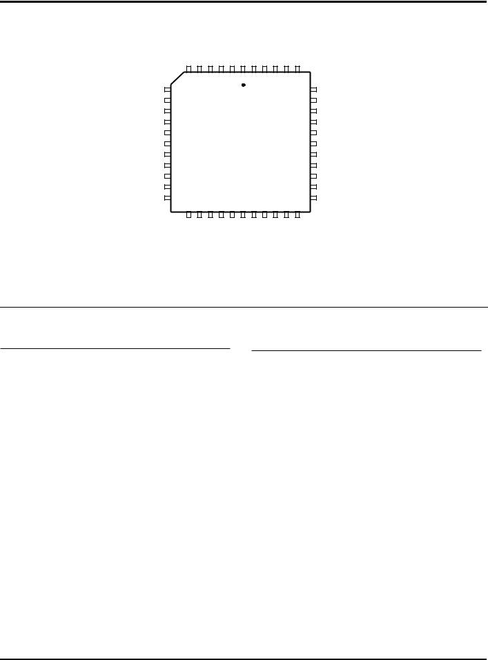
Figure 9. Standard Mode
28-Pin DIP/SOIC Pin Configuration*
|
Table 7. |
28-Pin DIP/SOIC/PLCC |
|
|
Pin Identification* |
|
|
|
|
|
|
Pin # |
Symbol |
Function |
Direction |
|
|
|
|
1-3 |
P25-P27 |
Port 2, Pins 5,6, |
In/Output |
|
|
|
|
4-7 |
P04-P07 |
Port 0, Pins 4,5,6,7 |
In/Output |
|
|
|
|
8 |
VCC |
Power Supply |
|
9 |
XTAL2 |
Crystal Oscillator |
Output |
|
|
|
|
10 |
XTAL1 |
Crystal Oscillator |
Input |
|
|
|
|
11-13 |
P31-P33 |
Port 3, Pins 1,2,3 |
Input |
|
|
|
|
14-15 |
P34-P35 |
Port 3, Pins 4,5 |
Output |
|
|
|
|
16 |
P37 |
Port 3, Pin 7 |
Output |
|
|
|
|
17 |
P36 |
Port 3, Pin 6 |
Output |
|
|
|
|
18 |
P30 |
Port 3, Pin 0 |
Input |
|
|
|
|
19-21 |
P00-P02 |
Port 0, Pins 0,1,2 |
In/Output |
|
|
|
|
22 |
VSS |
Ground |
|
23 |
P03 |
Port 0, Pin 3 |
In/Output |
|
|
|
|
24-28 |
P20-P24 |
Port 2, Pins |
In/Output |
|
|
0,1,2,3,4 |
|
|
|
|
|
Notes:
*Pin Identification and Configuration identical on DIP and Cerdip Window Lid style packages.
D5 |
|
1 |
28 |
|
D4 |
|
|||||
|
|||||
D6 |
|
|
|
|
D3 |
|
|
|
|
||
|
|
|
|
||
D7 |
|
|
|
|
D2 |
|
|
|
|
||
|
|
|
|
||
A4 |
|
|
|
|
D1 |
|
|
|
|
||
|
|
|
|
||
A5 |
|
|
|
|
D0 |
|
|
|
|
||
|
|
|
|
||
A6 |
|
|
|
|
A3 |
|
|
|
|
||
|
|
|
|
||
A7 |
|
|
28-Pin DIP |
|
VSS |
|
|
|
|||
|
|
|
|||
VCC |
|
|
|
|
A2 |
|
|
|
|
||
|
|
|
|
||
NC |
|
|
|
|
A1 |
|
|
|
|
||
|
|
|
|
||
/CE |
|
|
|
|
A0 |
|
|
|
|
||
|
|
|
|
||
/OE |
|
|
|
|
/PGM |
|
|
|
|
||
|
|
|
|
||
EPM |
|
|
|
|
A10 |
|
|
|
|
||
|
|
|
|
||
VPP |
|
14 |
15 |
|
A11 |
|
|
||||
|
|
||||
A8 |
|
|
A9 |
||
|
|||||
|
|||||
|
|
|
|
|
|
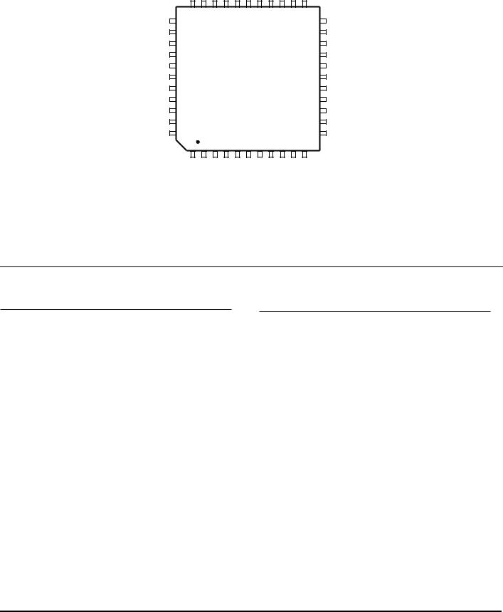
Figure 10. EPROM Programming Mode
28-Pin DIP/SOIC Pin Configuration*
|
P04 |
P27 |
P26 |
P25 |
P24 |
P23 |
P22 |
|
|
4 |
|
|
1 |
|
|
26 |
|
XXXP05 |
5 |
|
|
|
|
|
25 |
P21XXX |
XXXP06 |
|
|
|
|
|
|
|
XXXP20 |
XXXP07 |
|
28-Pin PLCC |
|
XXXP03 |
||||
VCCXXX |
|
|
XXXVSS |
|||||
XXXT2 |
|
|
|
|
|
|
|
XXXP02 |
XXXT1 |
|
|
|
|
|
|
|
XXXP01 |
XXXP31 |
11 |
|
|
|
|
|
19 |
P00XXX |
|
12 |
|
|
|
|
|
18 |
|
|
P32 |
P33 |
P34 |
P35 |
P37 |
P36 |
P30 |
|
Figure 11. Standard Mode
28-Pin PLCC Pin Configuration
10 |
P R E L I M I N A R Y |
DS97Z8X0500 |
|
Z86E30/E31/E40 |
Zilog |
Z8 4K OTP Microcontroller |
|
|
|
A4 |
D7 |
D6 |
D5 |
D4 |
D3 |
D2 |
|
|
4 |
|
|
1 |
|
|
26 |
|
XXXA5 |
5 |
|
|
|
|
|
25 |
D1XXX |
XXXA6 |
|
|
|
|
|
|
|
XXXD0 |
XXXA7 |
|
28-Pin PLCC |
|
XXXA3 |
||||
VCCXXX |
|
|
XXXVSS |
|||||
XXXNC |
|
|
|
|
|
|
|
A2XXX |
XXX/CE |
|
|
|
|
|
|
|
A1XXX |
XXX/OE |
11 |
|
|
|
|
|
19 |
XXXA0 |
|
12 |
|
|
|
|
|
18 |
|
|
EPM |
VPP |
A8 |
A9 |
A11 |
A10 |
/PGM |
|
Figure 12. EPROM Programming Mode
28-Pin PLCC Pin Configuration
Table 8. 28-Pin EPROM
Pin Identification*
Pin # |
Symbol |
Function |
Direction |
|
|
|
|
1-3 |
D5-D7 |
Data 5,6,7 |
In/Output |
|
|
|
|
4-7 |
A4-A7 |
Address 4,5,6,7 |
Input |
|
|
|
|
8 |
VCC |
Power Supply |
|
9 |
NC |
No connection |
|
|
|
|
|
10 |
/CE |
Chip Select |
Input |
|
|
|
|
11 |
/OE |
Output Enable |
Input |
|
|
|
|
12 |
EPM |
EPROM Prog. |
Input |
|
|
Mode |
|
|
|
|
|
13 |
VPP |
Prog. Voltage |
Input |
14-15 |
A8-A9 |
Address 8,9 |
Input |
|
|
|
|
16 |
A11 |
Address 11 |
Input |
|
|
|
|
17 |
A10 |
Address 10 |
Input |
|
|
|
|
18 |
/PGM |
Prog. Mode |
Input |
|
|
|
|
19-21 |
A0-A2 |
Address 0,1,2 |
Input |
|
|
|
|
22 |
VSS |
Ground |
|
23 |
A3 |
Address 3 |
Input |
|
|
|
|
24-28 |
D0-D4 |
Data 0,1,2,3,4 |
In/Output |
|
|
|
|
Notes:
*Pin Identification and Configuration identical on DIP and Cerdip Window Lid style packages.
DS97Z8X0500 |
P R E L I M I N A R Y |
11 |
Z86E30/E31/E40 |
|
|
|
|
Z8 4K OTP Microcontroller |
|
|
Zilog |
|
|
|
|
|
|
ABSOLUTE MAXIMUM RATINGS |
|
|
|
|
|
|
|
|
|
Parameter |
Min |
Max |
Units |
|
|
|
|
|
|
Ambient Temperature under Bias |
–40 |
+105 |
C |
|
|
|
|
|
|
Storage Temperature |
–65 |
+150 |
C |
|
|
|
|
|
|
Voltage on any Pin with Respect to VSS [Note 1] |
–0.6 |
+7 |
V |
|
Voltage on VDD Pin with Respect to VSS |
–0.3 |
+7 |
V |
|
Voltage on XTAL1 and /RESET Pins with Respect to VSS [Note 2] |
–0.6 |
VDD+1 |
V |
|
Total Power Dissipation |
|
1.21 |
W |
|
|
|
|
|
|
Maximum Allowable Current out of VSS |
|
220 |
mA |
|
Maximum Allowable Current into VDD |
|
180 |
mA |
|
Maximum Allowable Current into an Input Pin [Note 3] |
–600 |
+600 |
A |
|
|
|
|
|
|
Maximum Allowable Current into an Open-Drain Pin [Note 4] |
–600 |
+600 |
A |
|
|
|
|
|
|
Maximum Allowable Output Current Sinked by Any I/O Pin |
|
25 |
mA |
|
|
|
|
|
|
Maximum Allowable Output Current Sourced by Any I/O Pin |
|
25 |
mA |
|
|
|
|
|
|
Maximum Allowable Output Current Sinkedd by /RESET Pin |
|
3 mA |
|
|
|
|
|
|
|
Notes:
1.This applies to all pins except XTAL pins and where otherwise noted.
2.There is no input protection diode from pin to VDD.
3.This excludes XTAL pins.
4.Device pin is not at an output Low state.
Stresses greater than those listed under Absolute Maxi- |
Total power dissipation should not exceed 1.2 W for the |
mum Ratings may cause permanent damage to the de- |
package. Power dissipation is calculated as follows: |
vice. This is a stress rating only; functional operation of the |
Total Power Dissipation = VDD x [ IDD – (sum of IOH) ] |
device at any condition above those indicated in the oper- |
|
ational sections of these specifications is not implied. Ex- |
+ sum of [ (VDD – VOH) x IOH ] |
posure to absolute maximum rating conditions for an ex- |
+ sum of (V0L x I0L) |
tended period may affect device reliability. |
|
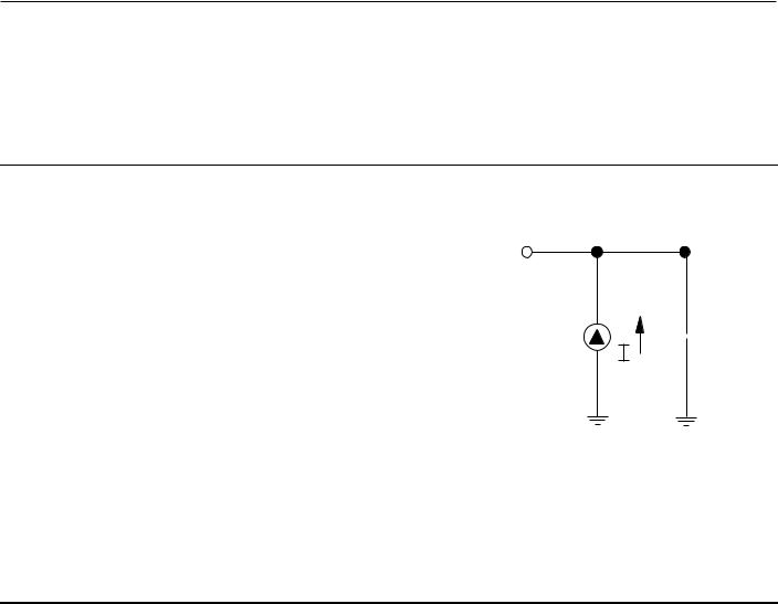
STANDARD TEST CONDITIONS
The characteristics listed below apply for standard test conditions as noted. All voltages are referenced to Ground. Positive current flows into the referenced pin (Test Load).
From Output
Under Test
 150 pF
Figure 13. Test Load Diagram
12 |
P R E L I M I N A R Y |
DS97Z8X0500 |

|
Z86E30/E31/E40 |
Zilog |
Z8 4K OTP Microcontroller |
|
|
CAPACITANCE
TA = 25°C, VCC = GND = 0V, f = 1.0 MHz; unmeasured pins returned to GND.
Parameter |
Min |
Max |
|
|
|
Input capacitance |
0 |
12 pF |
|
|
|
Output capacitance |
0 |
12 pF |
|
|
|
I/O capacitance |
0 |
12 pF |
|
|
|
DC ELECTRICAL CHARACTERISTICS
|
|
VCC |
TA= 0 °C to +70 °C |
Typical |
|
|
|
|
|
|
|
|
|
|
|
||
Sym |
Parameter |
Note [3] |
Min |
Max |
@ 25°C |
Units |
Conditions |
Notes |
|
|
|
|
|
|
|
|
|
VCH |
Clock Input High |
3.5V |
0.7 VCC |
VCC+0.3 |
1.8 |
V |
Driven by External |
|
|
Voltage |
5.5V |
0.7 VCC |
VCC+0.3 |
2.5 |
V |
Clock Generator |
|
VCL |
Clock Input Low |
3.5V |
GND-0.3 |
0.2 VCC |
0.9 |
V |
Driven by External |
|
|
Voltage |
4.5V |
GND-0.3 |
0.2 VCC |
1.5 |
V |
Clock Generator |
|
VIH |
Input High Voltage |
3.5V |
0.7 VCC |
VCC+0.3 |
2.5 |
V |
|
|
|
|
5.5V |
0.7 VCC |
VCC+0.3 |
2.5 |
V |
|
|
VIL |
Input Low Voltage |
3.5V |
GND-0.3 |
0.2 VCC |
1.5 |
V |
|
|
|
|
5.5V |
GND-0.3 |
0.2 VCC |
1.5 |
V |
|
|
VOH |
Output High Voltage |
3.5V |
VCC–0.4 |
|
3.3 |
V |
IOH = – 0.5 mA |
|
|
Low EMI Mode |
5.5V |
VCC -0.4 |
|
4.8 |
V |
|
|
VOH1 |
Output High Voltage |
3.5V |
VCC–0.4 |
|
3.3 |
V |
IOH = -2.0 mA |
|
|
|
5.5V |
VCC–0.4 |
|
4.8 |
V |
IOH = -2.0 mA |
|
VOL |
Output Low Voltage |
3.5V |
|
0.4 |
0.2 |
V |
IOL = 1.0 mA |
|
|
Low EMI Mode |
4.5V |
|
0.4 |
0.2 |
V |
IOL = 1.0 mA |
|
VOL1 |
Output Low Voltage |
3.5V |
|
0.4 |
0.1 |
V |
IOL = + 4.0 mA |
8 |
|
|
4.5V |
|
0.4 |
0.1 |
V |
IOL = + 4.0 mA |
8 |
VOL2 |
Output Low Voltage |
3.5V |
|
1.2 |
0.5 |
V |
IOL = + 12 mA |
8 |
|
|
4.5V |
|
1.2 |
0.5 |
V |
IOL = + 12 mA |
8 |
VRH |
Reset Input High |
3.5V |
.8 VCC |
VCC |
1.7 |
V |
|
|
|
Voltage |
5.5V |
.8 VCC |
VCC |
2.1 |
V |
|
|
VRL |
Reset Input Low |
3.5V |
GND –0.3 |
0.2 VCC |
1.3 |
V |
|
13 |
|
Voltage |
5.5V |
GND –0.3 |
0.2 VCC |
1.7 |
V |
|
|
VOLR |
Reset Output Low |
3.5V |
|
0.6 |
0.3 |
V |
IOL = 1.0 mA |
|
|
Voltage |
5.5V |
|
0.6 |
0.2 |
V |
IOL = 1.0 mA |
|
VOFFSET |
Comparator Input |
3.5V |
|
25 |
10 |
mV |
|
|
|
Offset Voltage |
4.5V |
|
25 |
10 |
mV |
|
|
|
|
|
|
|
|
|
|
|
VICR |
Input Common Mode |
3.5V |
0 |
VCC -1.0V |
|
V |
|
10 |
|
Voltage Range |
5.5V |
0 |
VCC -1.0V |
|
V |
|
10 |
IIL |
Input Leakage |
3.5V |
–1 |
2 |
0.032 |
A |
VIN = 0V, VCC |
|
|
|
4.5V |
–1 |
2 |
0.032 |
A |
VIN = 0V, VCC |
|
IOL |
Output Leakage |
3.5V |
–1 |
2 |
0.032 |
A |
VIN = 0V, VCC |
|
|
|
4.5V |
-1 |
2 |
0.032 |
A |
VIN = 0V, VCC |
|
IIR |
Reset Input Current |
3.5V |
–20 |
–130 |
–65 |
A |
|
|
|
|
4.5V |
–20 |
–180 |
–112 |
A |
|
|
|
|
|
|
|
|
|
|
|
DS97Z8X0500 |
P R E L I M I N A R Y |
13 |

Z86E30/E31/E40 |
|
|
|
|
|
|
|
|
Z8 4K OTP Microcontroller |
|
|
|
|
|
|
Zilog |
|
|
|
|
|
|
|
|
|
|
|
|
|
|
|
|
|
|
|
|
|
VCC |
TA= 0 °C to +70 °C |
Typical |
|
|
|
|
|
|
|
|
|
|
|
||
Sym |
Parameter |
Note [3] |
Min |
Max |
@ 25°C |
Units |
Conditions |
Notes |
|
|
|
|
|
|
|
|
|
ICC |
Supply Current |
3.5V |
|
20 |
7 |
mA |
@ 16 MHz |
4,5 |
|
|
5.5V |
|
25 |
20 |
mA |
@ 16 MHz |
4,5 |
ICC1 |
Standby Current |
3.5V |
|
8 |
3.7 |
mA |
VIN = 0V, VCC |
4,5 |
|
Halt Mode |
5.5V |
|
8 |
3.7 |
mA |
@ 16 MHz |
4,5 |
|
|
|
|
|
|
|
|
|
|
|
3.5V |
|
7.0 |
2.9 |
mA |
Clock Divide by |
4,5 |
|
|
5.5V |
|
7.0 |
2.9 |
mA |
16 @ 16 MHz |
4,5 |
|
|
|
|
|
|
|
|
|
ICC2 |
Standby Current |
3.5V |
|
10 |
2 |
A |
VIN = 0V, VCC |
6,11 |
|
Stop Mode |
5.5V |
|
10 |
3 |
A |
VIN = 0V, VCC |
6,11 |
|
|
3.5V |
|
800 |
600 |
A |
VIN = 0V, VCC |
6,11,14 |
|
|
5.5V |
|
800 |
600 |
A |
6,11,14 |
|
|
|
|
VIN = 0V, VCC |
|||||
|
|
|
|
|
|
|
|
|
IALL |
Auto Latch |
3.5V |
0.7 |
8 |
2.4 |
A |
0V <VIN<VCC |
9 |
|
Low Current |
5.5V |
1.4 |
15 |
4.7 |
A |
0V <VIN<VCC |
9 |
IALH |
Auto Latch |
3.5V |
–0.6 |
–5 |
–1.8 |
A |
0V<VIN<VCC |
9 |
|
High Current |
5.5V |
–1 |
–8 |
–3.8 |
A |
0V<VIN<VCC |
9 |
TPOR |
Power On Reset |
3.5V |
3.0 |
24 |
7 |
ms |
|
|
|
|
5.5V |
2.0 |
13 |
4 |
ms |
|
|
VLV |
Auto Reset Voltage |
|
2.3 |
3.1 |
2.9 |
V |
|
1,7 |
Notes:
1.Device does not function down to the Auto Reset voltage
2.GND=0V
3.The VCC voltage specification of 5.5V guarantees 5.0V ± 0.5V and the VCC voltage specification of 3.5V guarantees 3.5V only.
4.All outputs unloaded, I/O pins floating, inputs at rail.
5.CL1= CL2 = 22 pF
6.Same as note [4] except inputs at VCC
7.Max. temperature is 70°C
8.STD Mode (not Low EMI Mode)
9.Auto Latch (mask option) selected
10.For analog comparator inputs when analog comparators are enabled
11.Clock must be forced Low, when XTAL1 is clock driven and XTAL2 is floating
12.Typicals are at VCC = 5.0V and VCC = 3.5V
13.Z86C40 only
14.WDT running
14 |
P R E L I M I N A R Y |
DS97Z8X0500 |

|
|
|
|
|
|
|
|
Z86E30/E31/E40 |
||
Zilog |
|
|
|
|
|
|
Z8 4K OTP Microcontroller |
|||
|
|
|
|
|
|
|
|
|
|
|
|
|
|
|
|
|
|
|
|
|
|
|
|
|
|
TA=–40 °C to +105 °C |
|
|
|
|
|
|
|
|
|
VCC |
|
|
Typical |
|
|
|
|
|
Sym |
Parameter |
Note [3] |
Min |
Max |
@ 25°C |
Units |
Conditions |
Notes |
|
|
|
|
|
|
|
|
|
|
|
|
VCH |
Clock Input High |
4.5V |
0.7 VCC |
VCC+0.3 |
2.5 |
V |
Driven by External |
|
|
|
|
|
Voltage |
5.5V |
0.7 VCC |
VCC+0.3 |
2.5 |
V |
Clock Generator |
|
|
VCL |
Clock Input Low |
4.5V |
GND-0.3 |
0.2 VCC |
1.5 |
V |
Driven by External |
|
|
|
|
|
Voltage |
5.5V |
GND-0.3 |
0.2 VCC |
1.5 |
V |
Clock Generator |
|
|
VIH |
Input High Voltage |
4.5V |
0.7 VCC |
VCC+0.3 |
2.5 |
V |
|
|
|
|
|
|
|
5.5V |
0.7 VCC |
VCC+0.3 |
2.5 |
V |
|
|
|
VIL |
Input Low Voltage |
4.5V |
GND-0.3 |
0.2 VCC |
1.5 |
V |
|
|
|
|
|
|
|
5.5V |
GND-0.3 |
0.2 VCC |
1.5 |
V |
|
|
|
VOH |
Output High |
4.5V |
VCC–0.4 |
|
4.8 |
V |
IOH = – 0.5 mA |
8 |
|
|
|
|
Voltage Low EMI |
5.5V |
VCC–0.4 |
|
4.8 |
V |
IOH = – 0.5 mA |
8 |
|
|
|
Mode |
|
|
|
|
|
|
|
|
VOH1 |
Output High Voltage |
4.5V |
VCC–0.4 |
|
4.8 |
V |
IOH = -2.0 mA |
8 |
|
|
|
|
|
4.5V |
VCC–0.4 |
|
4.8 |
V |
IOH = -2.0 mA |
8 |
|
VOL |
Output Low Voltage |
4.5V |
|
0.4 |
0.2 |
V |
IOL = 1.0 mA |
|
|
|
|
|
Low EMI Mode |
5.5V |
|
0.4 |
0.2 |
V |
IOL = 1.0 mA |
|
|
VOL1 |
Output Low Voltage |
4.5V |
|
0.4 |
0.1 |
V |
IOL = + 4.0 mA |
8 |
|
|
|
|
|
5.5V |
|
0.4 |
0.1 |
V |
IOL = +4.0 mA |
8 |
|
|
VOL2 |
Output Low Voltage |
4.5V |
|
1.2 |
0.5 |
V |
IOL = + 12 mA |
8 |
|
|
|
|
5.5V |
|
1.2 |
0.5 |
V |
IOL = + 12 mA |
8 |
|
|
VRH |
Reset Input High |
3.5V |
.8 VCC |
VCC |
1.7 |
V |
|
13 |
|
|
|
Voltage |
5.5V |
.8 VCC |
VCC |
2.1 |
V |
|
13 |
|
VOLR |
Reset Output Low |
3.5V |
|
0.6 |
0.3 |
V |
IOL = 1.0 mA |
13 |
|
|
|
|
Voltage |
5.5V |
|
0.6 |
0.2 |
V |
IOL = 1.0 mA |
13 |
|
VOFFSET Comparator Input |
4.5V |
|
25 |
10 |
mV |
|
|
|
||
|
|
Offset Voltage |
5.5V |
|
25 |
10 |
mV |
|
|
|
|
|
|
|
|
|
|
|
|
|
|
VICR |
Input Common |
4.5V |
0 |
VCC-1.5V |
|
V |
|
10 |
|
|
|
|
Mode Voltage |
5.5V |
0 |
VCC-1.5V |
|
V |
|
10 |
|
|
|
Range |
|
|
|
|
|
|
|
|
IIL |
Input Leakage |
4.5V |
–1 |
2 |
<1 |
A |
VIN = 0V, VCC |
|
|
|
|
|
|
5.5V |
–1 |
2 |
<1 |
A |
VIN = 0V, VCC |
|
|
IOL |
Output Leakage |
4.5V |
–1 |
2 |
<1 |
A |
VIN = 0V, VCC |
|
|
|
|
|
|
5.5V |
–1 |
2 |
<1 |
A |
VIN = 0V, VCC |
|
|
IIR |
Reset Input Current |
4.5V |
–18 |
–180 |
–112 |
A |
|
|
|
|
|
|
|
5.5V |
–18 |
–180 |
–112 |
A |
|
|
|
|
|
|
|
|
|
|
|
|
|
|
ICC |
Supply Current |
4.5V |
|
25 |
20 |
mA |
@ 16 MHz |
4,5 |
|
|
|
|
|
5.5V |
|
25 |
20 |
mA |
@ 16 MHz |
4,5 |
|
|
ICC1 |
Standby Current |
4.5V |
|
8 |
3.7 |
mA |
VIN = 0V, VCC |
4,5 |
|
|
|
Halt Mode |
5.5V |
|
8 |
3.7 |
mA |
@ 16 MHz |
4,5 |
|
|
|
|
|
VIN = 0V, VCC |
|
|||||
|
|
|
|
|
|
|
|
@ 16 MHz |
|
|
|
|
|
|
|
|
|
|
|
|
|
ICC2 |
Standby Current |
4.5V |
|
10 |
2 |
A |
VIN = 0V, VCC |
6,11,14 |
|
|
|
|
(Stop Mode) |
5.5V |
|
10 |
3 |
A |
VIN = 0V, VCC |
6,11,14 |
|
IALL |
Auto Latch Low |
4.5V |
1.4 |
20 |
4.7 |
A |
0V < VIN < VCC |
9 |
|
|
|
|
Current |
5.5V |
1.4 |
20 |
4.7 |
A |
0V < VIN < VCC |
9 |
|
DS97Z8X0500 |
P R E L I M I N A R Y |
15 |

Z86E30/E31/E40 |
|
|
|
|
|
|
|
|
||
Z8 4K OTP Microcontroller |
|
|
|
|
|
|
Zilog |
|||
|
|
|
|
|
|
|
|
|
|
|
|
|
|
|
|
|
|
|
|
|
|
|
|
|
|
TA=–40 °C to +105 °C |
|
|
|
|
|
|
|
|
|
VCC |
|
|
Typical |
|
|
|
|
|
Sym |
Parameter |
Note [3] |
Min |
Max |
@ 25°C |
Units |
Conditions |
Notes |
|
|
|
|
|
|
|
|
|
|
|
|
IALH |
Auto Latch High |
4.5V |
–1.0 |
–10 |
–3.8 |
A 0V < VIN < VCC |
9 |
|
||
|
|
Current |
5.5V |
–1.0 |
–10 |
–3.8 |
A |
0V < VIN < VCC |
9 |
|
|
TPOR |
Power On Reset |
4.5V |
2.0 |
14 |
4 |
mS |
|
|
|
|
|
|
5.5V |
2.0 |
14 |
4 |
mS |
|
|
|
|
VLV |
Auto Reset Voltage |
|
2.0 |
3.3 |
2.9 |
V |
|
1 |
|
1.Device does not function down to the Auto Reset voltage
2.GND=0V
3.The VCC voltage spec. of 5.5V guarantees 5.0V +/- ± 0.5V
4.All outputs unloaded, I/O pins floating, inputs at rail
5.CL1= CL2 = 22 pF
6.Same as note [4] except inputs at VCC
7.Max. temperature is 70°C
8.STD Mode (not Low EMI Mode)
9.Auto Latch (mask option) selected
10.For analog comparator inputs when analog comparators are enabled
11.Clock must be forced Low, when XTAL1 is clock driven and XTAL2 is floating
12.Typicals are at VCC = 5.0V
13.Z86C40 only
14.WDT is not running
16 |
P R E L I M I N A R Y |
DS97Z8X0500 |

|
|
|
Z86E30/E31/E40 |
Zilog |
|
|
Z8 4K OTP Microcontroller |
R//W , /DM |
|
|
|
|
|
|
13 |
12 |
|
|
19 |
|
|
|
|
Port 0 |
|
|
|
|
16 |
|
20 |
|
|
|
|
18 |
3 |
|
|
Port 1 |
A7 - A0 |
|
D7 - D0 IN |
1 |
2 |
|
9 |
/AS |
|
|
|
|
8 |
|
1 1 |
4 |
|
|
|
|
5 |
6 |
|
/DS |
|
|
|
(Read) |
17 |
|
|
|
|
|
|
|
|
|
10 |
Port1 |
A7 - A0 |
D7 - D0 |
OUT |
|
14 |
|
15 |
|
|
|
7 |
/DS |
|
|
|
(W rite) |
|
|
|
Figure 14. External I/O or Memory Read/Write Timing
Z86C40 Only
DS97Z8X0500 |
P R E L I M I N A R Y |
17 |

Z86E30/E31/E40 |
|
|
|
|
|
|
|
|
Z8 4K OTP Microcontroller |
|
|
|
|
Zilog |
|||
|
|
|
|
|
|
|
|
|
|
|
|
|
|
|
|
|
|
|
|
|
|
TA = 0°C to 70°C |
|
|
|
|
|
|
|
Note [3] |
|
16 MHz |
|
|
|
|
|
|
|
|
|
|
|
|
No |
Symbol |
Parameter |
VCC |
Min |
Max |
Units |
Notes |
|
1 |
TdA(AS) |
Address Valid to /AS Rise |
3.5V |
25 |
|
ns |
2 |
|
|
|
Delay |
5.5V |
25 |
|
ns |
|
|
|
|
|
|
|
|
|
|
|
2 |
TdAS(A) |
/AS Rise to Address Float |
3.5V |
35 |
|
ns |
2 |
|
|
|
Delay |
5.5V |
35 |
|
ns |
|
|
|
|
|
|
|
|
|
|
|
3 |
TdAS(DR) |
/AS Rise to Read Data |
3.5V |
|
180 |
ns |
1,2 |
|
|
|
Req’d Valid |
5.5V |
|
180 |
ns |
|
|
|
|
|
|
|
|
|
|
|
4 |
TwAS |
/AS Low Width |
3.5V |
40 |
|
ns |
2 |
|
|
|
|
5.5V |
40 |
|
ns |
|
|
|
|
|
|
|
|
|
|
|
5 |
TdAS(DS) |
Address Float to /DS Fall |
3.5V |
0 |
|
ns |
|
|
|
|
|
5.5V |
0 |
|
ns |
|
|
|
|
|
|
|
|
|
|
|
6 |
TwDSR |
/DS (Read) Low Width |
3.5V |
135 |
|
ns |
1,2 |
|
|
|
|
5.5V |
135 |
|
ns |
|
|
|
|
|
|
|
|
|
|
|
7 |
TwDSW |
/DS (Write) Low Width |
3.5V |
80 |
|
ns |
1,2 |
|
|
|
|
5.5V |
80 |
|
ns |
|
|
|
|
|
|
|
|
|
|
|
8 |
TdDSR(DR) |
/DS Fall to Read Data Req’d |
3.5V |
|
75 |
ns |
1,2 |
|
|
|
Valid |
5.5V |
|
75 |
ns |
|
|
|
|
|
|
|
|
|
|
|
9 |
ThDR(DS) |
Read Data to /DS Rise Hold |
3.5V |
0 |
|
ns |
2 |
|
|
|
Time |
5.5V |
0 |
|
ns |
|
|
|
|
|
|
|
|
|
|
|
10 |
TdDS(A) |
/DS Rise to Address Active |
3.5V |
50 |
|
ns |
2 |
|
|
|
Delay |
5.5V |
50 |
|
ns |
|
|
|
|
|
|
|
|
|
|
|
11 |
TdDS(AS) |
/DS Rise to /AS Fall Delay |
3.5V |
35 |
|
ns |
2 |
|
|
|
|
5.5V |
35 |
|
ns |
|
|
|
|
|
|
|
|
|
|
|
12 |
TdR/W(AS) |
R//W Valid to /AS Rise |
3.5V |
25 |
|
ns |
2 |
|
|
|
Delay |
5.5V |
25 |
|
ns |
|
|
|
|
|
|
|
|
|
|
|
13 |
TdDS(R/W) |
/DS Rise to R//W Not Valid |
3.5V |
35 |
|
ns |
2 |
|
|
|
|
5.5V |
35 |
|
ns |
|
|
|
|
|
|
|
|
|
|
|
14 |
TdDW(DSW) |
Write Data Valid to /DS Fall |
3.5V |
55 |
25 |
ns |
2 |
|
|
|
(Write) Delay |
5.5V |
55 |
25 |
ns |
|
|
|
|
|
|
|
|
|
|
|
15 |
TdDS(DW) |
/DS Rise to Write Data Not |
3.5V |
35 |
|
ns |
2 |
|
|
|
Valid Delay |
5.5V |
35 |
|
ns |
|
|
|
|
|
|
|
|
|
|
|
16 |
TdA(DR) |
Address Valid to Read Data |
3.5V |
|
230 |
ns |
1,2 |
|
|
|
Req’d Valid |
5.5V |
|
230 |
ns |
|
|
|
|
|
|
|
|
|
|
|
17 |
TdAS(DS) |
/AS Rise to /DS Fall Delay |
3.5V |
45 |
|
ns |
2 |
|
|
|
|
5.5V |
45 |
|
ns |
|
|
|
|
|
|
|
|
|
|
|
18 |
TdDM(AS) |
/DM Valid to /AS Fall Delay |
3.5V |
30 |
|
ns |
2 |
|
|
|
|
5.5V |
30 |
|
ns |
|
|
|
|
|
|
|
|
|
|
|
20 |
ThDS(AS) |
/DS Valid to Address Valid |
3.5V |
35 |
|
ns |
|
|
|
|
Hold Time |
5.5V |
35 |
|
ns |
|
|
|
|
|
|
|
|
|
|
|
Notes:
1.When using extended memory timing add 2 TpC
2.Timing numbers given are for minimum TpC
3.The VCC voltage specification of 5.5V guarantees 5.0V +/- ±0.5V and the VCC voltage specification of 3.5V guarantees 3.5V only
Standard Test Load
All timing references use 0.7 VCC for a logic 1 and 0.2 VCC for a logic 0
For Standard Mode (not Low-EMI Mode for outputs) with SMR D1 = 0, D0 = 0
18 |
P R E L I M I N A R Y |
DS97Z8X0500 |

|
|
|
|
|
|
Z86E30/E31/E40 |
||
Zilog |
|
|
|
|
Z8 4K OTP Microcontroller |
|||
|
|
|
|
|
|
|
|
|
|
|
|
|
|
|
|
|
|
|
|
|
TA = -40°C to 105°C |
|
|
|
|
|
|
|
|
|
16 MHz |
|
|
|
|
|
|
|
Note [3] |
|
|
|
|
|
No |
Symbol |
Parameter |
VCC |
Min |
Max |
Units |
Notes |
|
1 |
TdA(AS) |
Address Valid to /AS Rise |
4.5V |
25 |
|
ns |
2 |
|
|
|
Delay |
5.5V |
25 |
|
ns |
|
|
|
|
|
|
|
|
|
|
|
2 |
TdAS(A) |
/AS Rise to Address Float |
4.5V |
35 |
|
ns |
2 |
|
|
|
Delay |
5.5V |
35 |
|
ns |
|
|
|
|
|
|
|
|
|
|
|
3 |
TdAS(DR) |
/AS Rise to Read Data |
4.5V |
|
180 |
ns |
1,2 |
|
|
|
Req’d Valid |
5.5V |
|
180 |
ns |
|
|
|
|
|
|
|
|
|
|
|
4 |
TwAS |
/AS Low Width |
4.5V |
40 |
|
ns |
2 |
|
|
|
|
5.5V |
40 |
|
ns |
|
|
|
|
|
|
|
|
|
|
|
5 |
TdAS(DS) |
Address Float to /DS Fall |
4.5V |
0 |
|
ns |
|
|
|
|
|
5.5V |
0 |
|
ns |
|
|
|
|
|
|
|
|
|
|
|
6 |
TwDSR |
/DS (Read) Low Width |
4.5V |
135 |
|
ns |
1,2 |
|
|
|
|
5.5V |
135 |
|
ns |
|
|
|
|
|
|
|
|
|
|
|
7 |
TwDSW |
/DS (Write) Low Width |
4.5V |
80 |
|
ns |
1,2 |
|
|
|
|
5.5V |
80 |
|
ns |
|
|
|
|
|
|
|
|
|
|
|
8 |
TdDSR(DR) |
/DS Fall to Read Data Req’d |
4.5V |
|
75 |
ns |
1,2 |
|
|
|
Valid |
5.5V |
|
75 |
ns |
|
|
|
|
|
|
|
|
|
|
|
9 |
ThDR(DS) |
Read Data to /DS Rise Hold |
4.5V |
0 |
|
ns |
2 |
|
|
|
Time |
5.5V |
0 |
|
ns |
|
|
|
|
|
|
|
|
|
|
|
10 |
TdDS(A) |
/DS Rise to Address Active |
4.5V |
50 |
|
ns |
2 |
|
|
|
Delay |
5.5V |
50 |
|
ns |
|
|
|
|
|
|
|
|
|
|
|
11 |
TdDS(AS) |
/DS Rise to /AS Fall Delay |
4.5V |
35 |
|
ns |
2 |
|
|
|
|
5.5V |
35 |
|
ns |
|
|
|
|
|
|
|
|
|
|
|
12 |
TdR/W(AS) |
R//W Valid to /AS Rise |
4.5V |
25 |
|
ns |
2 |
|
|
|
Delay |
5.5V |
25 |
|
ns |
|
|
|
|
|
|
|
|
|
|
|
13 |
TdDS(R/W) |
/DS Rise to R//W Not Valid |
4.5V |
35 |
|
ns |
2 |
|
|
|
|
5.5V |
35 |
|
ns |
|
|
|
|
|
|
|
|
|
|
|
14 |
TdDW(DSW) |
Write Data Valid to /DS Fall |
4.5V |
55 |
25 |
ns |
2 |
|
|
|
(Write) Delay |
5.5V |
55 |
25 |
ns |
|
|
|
|
|
|
|
|
|
|
|
15 |
TdDS(DW) |
/DS Rise to Write Data Not |
4.5V |
35 |
|
ns |
2 |
|
|
|
Valid Delay |
5.5V |
35 |
|
ns |
|
|
|
|
|
|
|
|
|
|
|
16 |
TdA(DR) |
Address Valid to Read Data |
4.5V |
|
230 |
ns |
1,2 |
|
|
|
Req’d Valid |
5.5V |
|
230 |
ns |
|
|
|
|
|
|
|
|
|
|
|
17 |
TdAS(DS) |
/AS Rise to /DS Fall Delay |
4.5V |
45 |
|
ns |
2 |
|
|
|
|
5.5V |
45 |
|
ns |
|
|
|
|
|
|
|
|
|
|
|
18 |
TdDM(AS) |
/DM Valid to /AS Fall Delay |
4.5V |
30 |
|
ns |
2 |
|
|
|
|
5.5V |
30 |
|
ns |
|
|
|
|
|
|
|
|
|
|
|
20 |
ThDS(AS) |
/DS Valid to Address Valid |
4.5V |
35 |
|
ns |
|
|
|
|
Hold Time |
5.5V |
35 |
|
ns |
|
|
|
|
|
|
|
|
|
|
|
Notes:
1.When using extended memory timing add 2 TpC
2.Timing numbers given are for minimum TpC
3.The VCC voltage specification of 5.5V guarantees 5.0V +/- 0.5V and the VCC voltage specification of 3.5V guarantees 3.5V only
Standard Test Load
All timing references use 0.7 VCC for a logic 1 and 0.2 VCC for a logic 0
For Standard Mode (not Low-EMI Mode for outputs) with SMR D1 = 0, D0 = 0
DS97Z8X0500 |
P R E L I M I N A R Y |
19 |
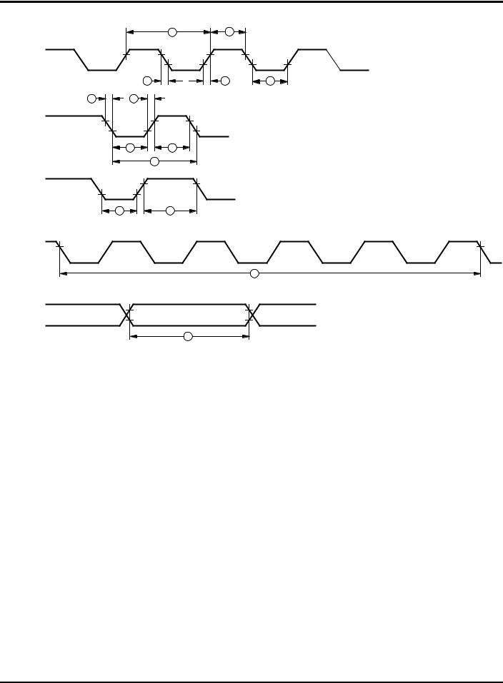
Z86E30/E31/E40 |
|
|
|
Z8 4K OTP Microcontroller |
|
|
Zilog |
|
|
1 |
3 |
Clock |
|
|
|
|
2 |
2 |
3 |
7 |
7 |
|
|
TIN |
|
|
|
|
4 |
5 |
|
|
|
6 |
|
IRQN |
|
|
|
8 |
|
9 |
|
Clock
Setup
11
Stop
Mode
Recovery
Source
10
Figure 15. Additional Timing Diagram
20 |
P R E L I M I N A R Y |
DS97Z8X0500 |
Loading...