


ZILOG Z86C0208PEC, Z86C0208PSC, Z86C0208SEC, Z86C0208SSC, Z86E0208PSC Datasheet
...PRELIMINARY CUSTOMER PROCUREMENT SPECIFICATION
1
Z86C02/E02/L02 1
LOW-COST, 512-BYTE ROM
MICROCONTROLLERS
FEATURES
|
ROM |
RAM* |
Speed |
Auto |
Permanent |
Device |
(KB) |
(Bytes) |
(MHz) |
Latch |
WDT |
|
|
|
|
|
|
Z86C02 |
512 |
61 |
8 |
Optional |
Optional |
|
|
|
|
|
|
Z86E02 |
512 |
61 |
8 |
Optional |
Optional |
|
|
|
|
|
|
Z86L02 |
512 |
61 |
8 |
Optional |
Optional |
|
|
|
|
|
|
Note: *General-Purpose
■18-Pin DIP and SOIC Packages
■0°C to 70°C Standard Temperature –40°C to 105°C Extended Temperature
(Z86C02/E02 only)
■3.0V to 5.5V Operating Range (Z86C02)
4.5V to 5.5V Operating Range (Z86E02)
2.0V to 3.9V Operating Range (Z86L02)
■14 Input / Output Lines
■Five Vectored, Prioritized Interrupts from Five Different Sources
■Two On-Board Comparators
■Software Enabled Watch-Dog Timer (WDT)
■Programmable Interrupt Polarity
■Two Standby Modes: STOP and HALT
■Low-Voltage Protection
■ROM Mask/OTP Options:
–Low-Noise (Z86C02/E02 only)
–ROM Protect
–Auto Latch
–Permanent Watch-Dog Timer (WDT)
–RC Oscillator (Z86C02/L02 Only)
–32 KHz Operation (Z86C02/L02 Only)
■One Programmable 8-Bit Counter/Timer with a 6-Bit Programmable Prescaler
■Power-On Reset (POR) Timer
■On-Chip Oscillator that Accepts RC, Crystal, Ceramic Resonator, LC, or External Clock Drive (C02/L02 only)
■On-Chip Oscillator that Accepts RC or External Clock Drive (Z86E02 SL1903 only)
■On-Chip Oscillator that Accepts Crystal, Ceramic Resonator, LC, or External Clock Drive (Z86E02 only)
■Clock-Free WDT Reset
■Low-Power Consumption (50mw)
■Fast Instruction Pointer (1.5 s @ 8 MHz)
■Fourteen Digital Inputs at CMOS Levels; Schmitt-Triggered
GENERAL DESCRIPTION
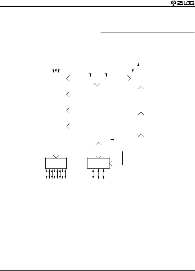
Zilog's Z86C02/E02/L02 microcontrollers (MCUs) are members of the Z8® single-chip MCU family, which offer easy software/hardware system expansion.
For applications demanding powerful I/O capabilities, the MCU's dedicated input and output lines are grouped into
three ports, and are configurable under software control to provide timing, status signals, or parallel I/O.
One on-chip counter/timer, with a large number of user-se- lectable modes, off-load the system of administering realtime tasks such as counting/timing and I/O data communi-
DS96DZ80301 (11/96) |
P R E L I M I N A R Y |
1-1 |
Z86C02/E02/L02
Low-Cost, 512-Byte ROM Microcontrollers
GENERAL DESCRIPTION (Continued)
cations. Additionally, two on-board comparators process analog signals with a common reference voltage (Figure 1).
Note: All Signals with a preceding front slash, "/", are active Low, e.g.: B//W (WORD is active Low); /B/W (BYTE is active Low, only).
Power connections follow conventional descriptions below:
Connection |
Circuit |
Device |
|
|
|
Power |
VCC |
VDD |
Ground |
GND |
VSS |
Input |
|
|
|
|
|
|
|
|
|
|
|
|
|
|
|
|
|
|
XTAL |
|||||||||||||||
|
|
|
|
|
|
|
|
|
|
Vcc |
GND |
|
|
|
||||||||||||||||||||
|
|
|
|
|
|
|
|
|
|
|
||||||||||||||||||||||||
|
|
|
|
|
|
|
|
|
|
|
|
|
|
|
|
|
|
|
|
|
|
|
|
|
|
|
|
|
|
|
|
|
|
|
|
|
|
|
|
|
|
|
|
|
|
|
|
|
|
|
|
|
|
|
|
|
|
|
|
|
|
|
|
|
|
|
|
|
|
|
|
|
|
|
|
|
|
|
|
|
|
|
|
|
|
|
|
|
|
|
|
|
|
|
|
|
|
|
|
|
|
|
|
|
Port 3 |
|
|
|
|
|
|
|
|
|
|
|
|
|
|
|
|
|
|
|
|
|
|
|
|
Machine |
|||||||||
|
|
|
|
|
|
|
|
|
|
|
|
|
|
|
|
|
|
|
|
|
|
Timing & Inst. |
||||||||||||
|
|
|
|
|
|
|
|
|
|
|
|
|
|
|
|
|
|
|
|
|
|
|
|
|
|
|
|
|
|
Control |
||||
|
|
|
|
|
|
|
|
|
|
|
|
|
|
|
|
|
|
|
|
|
|
|
|
|
|
|
|
|
|
|
|
|
|
|
|
|
|
|
|
|
|
|
|
|
|
|
|
|
|
|
|
|
|
|
|
|
|
|
|
|
|
|
|
|
|
|
|
|
|
Counter/ |
|
|
|
|
|
|
ALU |
|
|
|
|
|
|
|
|
|
|
|
|
|
|
|
|
|
||||||||||
Timer |
|
|
|
|
|
|
|
|
|
|
|
|
|
|
|
|
|
|
|
|
|
|
|
|
|
|
|
|
|
|||||
|
|
|
|
|
|
|
|
|
|
|
|
|
|
|
|
|
|
|
|
|
|
|
|
|
|
|
|
|
||||||
|
|
|
|
|
|
|
|
|
|
|
|
|
|
|
|
|
|
|
|
|
|
|
|
|
|
|
|
|
|
|
|
|
|
|
|
|
|
|
|
|
|
|
|
|
|
|
|
|
|
|
|
|
|
|
|
|
|
|
|
|
|
|
|
|
|
||||
|
|
|
|
|
|
|
|
|
|
|
FLAG |
|
|
|
|
|
|
|
|
|
|
|
|
Program |
||||||||||
Interrupt |
|
|
|
|
|
|
|
|
|
|
|
|
|
|
||||||||||||||||||||
|
|
|
|
|
|
|
|
|
|
|
|
|
|
|
|
|
|
|
|
|
|
|
|
Memory |
||||||||||
Control |
|
|
|
|
|
|
|
|
|
|
|
|
|
|
|
|
|
|
|
|
|
|
|
|
|
|
|
|
|
|||||
|
|
|
|
|
|
|
|
|
|
|
|
|
|
|
|
|
|
|
|
|
|
|
|
|
|
|
|
|
|
|
|
|
|
|
|
|
|
|
|
|
|
|
|
|
|
Register |
|
|
|
|
|
|
|
|
|
|
|
|
|
|
|
|
|
||||||
|
|
|
|
|
|
|
|
|
|
|
Pointer |
|
|
|
|
|
|
|
|
|
|
|
|
|
|
|
|
|
||||||
Two Analog |
|
|
|
|
|
|
|
|
|
|
|
|
|
|
|
|
|
|
|
|
|
|
|
|
Program |
|||||||||
|
|
|
|
|
|
|
|
|
|
|
|
|
|
|
|
|
|
|
|
|
|
|||||||||||||
Comparators |
|
|
|
|
General-Purpose |
|
|
|
|
|
|
|
|
|
|
Counter |
||||||||||||||||||
|
|
|
|
|
|
|
|
|
|
|
|
|
|
|
|
|
|
|
|
|
|
|
|
|
||||||||||
|
|
|
|
|
|
|
|
|
|
Register File |
|
|
|
|
|
|
|
|
|
|
|
|
|
|
|
|||||||||
|
|
|
|
|
|
|
|
|
|
|
|
|
|
|
|
|
|
|
|
|
|
|
|
|
|
|
|
|
|
|
|
|
|
|
|
|
|
|
|
|
|
|
|
|
|
|
|
|
|
|
|
|
|
|
|
|
|
|
|
|
|
|
|
|
|
|
|
|
|
|
|
|
|
|
|
|
|
|
|
|
|
|
|
|
|
|
|
|
|
|
|
|
|
|
|
|
|
|
|
|
|
|
|
|
|
|
|
|
|
|
|
|
|
|
|
|
|
|
|
|
|
|
|
|
|
|
|
|
|
|
|
|
|
|
|
|
|
|
|
|
|
|
|
|
|
|
|
|
|
|
|
|
|
|
|
|
|
|
|
|
|
|
|
|
|
|
|
|
|
|
|
|
|
|
|
|
|
|
|
|
|
|
|
|
|
|
|
|
|
|
|
|
|
|
|
|
|
|
|
|
|
|
|
|
|
|
|
|
|
|
|
|
|
|
|
|
|
|
|
|
|
|
|
|
|
|
|
|
|
|
|
|
|
|
|
|
|
|
|
|
|
|
|
|
|
|
|
|
|
|
|
|
|
|
|
|
|
|
|
|
|
|
|
|
|
|
|
|
|
|
|
|
|
|
|
|
|
|
|
Port 2 |
Port 0 |
I/O |
I/O |
(Bit Programmable) |
|
Figure 1. Z86C02/E02/L02 Functional Block Diagram
1-2 |
P R E L I M I N A R Y |
DS96DZ80301 (11/96) |

Z86C02/E02/L02
Low-Cost, 512-Byte ROM Microcontrollers
GENERAL DESCRIPTION (Continued)
|
MUX |
D7-D0 |
|
|
|
Z8 MCU |
|
|
|
||
|
|
|
|
||
A10-A0 |
Address |
A10-A0 |
|
|
|
|
MUXData |
PORT2Z8 |
|||
Address |
EPROM |
||||
|
|
|
|||
Counter |
|
|
|
||
|
D7-D0 |
|
|
||
A10-A0 |
|
|
|
||
|
|
|
|
||
3 Bits |
|
Option Bits |
|
|
|
|
|
|
|
D7-D0 |
|
PGM |
|
|
|
|
|
Mode Logic |
|
|
|
|
Clear |
Clock |
EPM |
/CE |
/PGM |
VPP |
/OE |
P00 |
P01 |
P32 |
XT1 |
P02 |
P33 |
P31 |
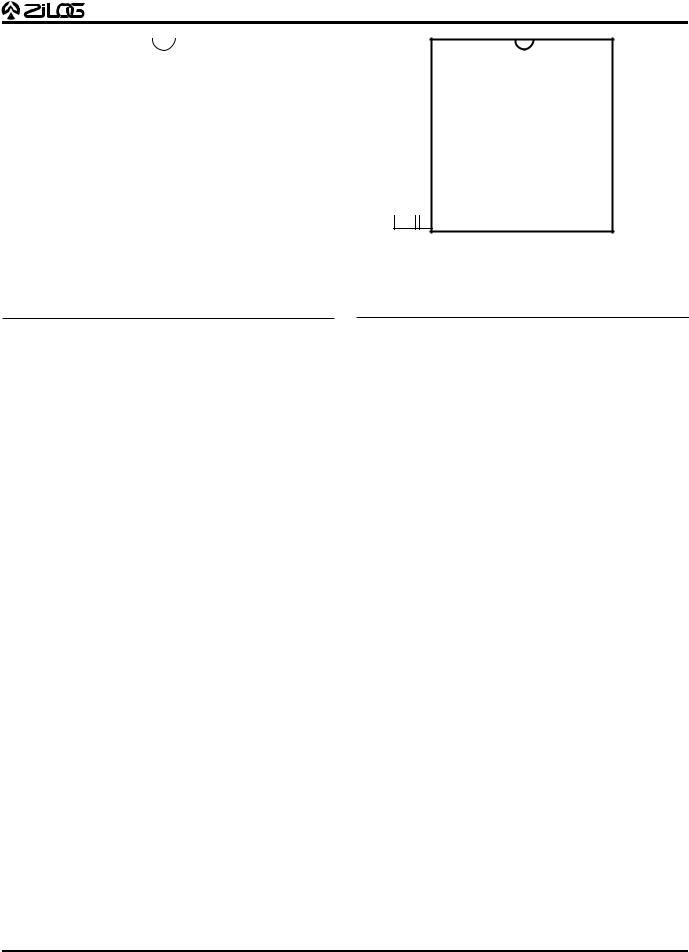
Figure 2. EPROM Programming Mode Block Diagram
PIN DESCRIPTIONS
|
|
|
|
|
|
Table 1. 18-Pin Standard Mode Identification |
|||
P24 |
|
1 |
18 |
|
P23 |
||||
|
|
|
|
|
|
||||
|
|
Pin # |
Symbol |
Function |
Direction |
||||
P25 |
|
2 |
17 |
|
P22 |
||||
|
|
||||||||
|
|
|
|
|
|
||||
|
|
|
|
|
|
|
|
|
|
P26 |
|
3 |
16 |
|
P21 |
1-4 |
P24-P27 |
Port 2, Pins 4, 5, 6, 7 |
In/Output |
|
|
||||||||
|
|
|
|
|
|
||||
P27 |
|
4 |
15 |
|
P20 |
5 |
VCC |
Power Supply |
|
|
|
|
|||||||
|
|
|
|
|
|||||
Vcc |
|
5 |
14 |
|
GND |
6 |
XTAL2 |
Crystal Oscillator |
Output |
|
|
||||||||
XTAL2 |
|
6 |
13 |
|
P02 |
|
|
Clock |
|
|
|
|
|
|
|||||
|
|
|
|
|
|
||||
XTAL1 |
|
7 |
12 |
|
P01 |
7 |
XTAL1 |
Crystal Oscillator |
Input |
|
|
||||||||
|
|
|
|
Clock |
|
||||
P31 |
|
8 |
11 |
|
P00 |
|
|
|
|
|
|
8 |
P31 |
Port 3, Pin 1, AN1 |
Input |
||||
P32 |
|
9 |
10 |
|
P33 |
||||
|
|
|
|
|
|
9 |
P32 |
Port 3, Pin 2, AN2 |
Input |
|
|
|
|
|
|
|
|
|
|
|
|
Standard Mode |
|
|
10 |
P33 |
Port 3, Pin 3, REF |
Input |
|
|
|
|
|
|
|
|
|
|
|
|
|
|
|
|
|
11-13 |
P00-P02 |
Port 0, Pins 0, 1, 2 |
In/Output |
|
|
|
|
|
|
|
|
|
|
|
|
|
|
|
|
14 |
GND |
Ground |
|
|
|
|
|
|
|
|
|
|
|
Figure 3. 18-Pin Standard Mode Configuration |
15-18 |
P20-P23 |
Port 2, Pins 0, 1, 2, 3 |
In/Output |
|||||
|
|
|
|
||||||
1-3 |
P R E L I M I N A R Y |
DS96DZ80301 (11/96) |
Z86C02/E02/L02
Low-Cost, 512-Byte ROM Microcontrollers
D4 |
|
1 |
18 |
|
D3 |
P24 |
|
|
|
|
1 |
18 |
|
|
|
P23 |
|
|
|
|
|
|
|
|
|
||||||||
|
|
|
|
|||||||||||||
D5 |
|
2 |
17 |
|
D2 |
|
|
|
|
|
|
|
|
|
|
|
|
|
P25 |
2 |
17 |
|
|
|
P22 |
||||||||
D6 |
|
3 |
16 |
|
D1 |
|
|
|
|
|
|
16 |
|
|
|
|
|
|
|
|
|
|
|
|
|
|
|
|
|||||
|
|
|
|
|
|
|
|
|
|
|
|
|||||
|
|
P26 |
3 |
|
|
|
P21 |
|||||||||
D7 |
|
4 |
15 |
|
D0 |
|
|
|
|
|
|
|
|
|
|
|
|
|
|
|
|
|
|
|
|
|
|
|
|
||||
Vcc |
|
5 |
14 |
|
GND |
P27 |
|
|
|
4 |
15 |
|
|
|
P20 |
|
|
|
VCC |
|
|
|
|
5 |
14 |
|
|
|
GND |
||||
N/C |
|
6 |
13 |
|
/PGM |
|
|
|
|
|
|
|
||||
/CE |
|
7 |
12 |
|
CLOCK |
XTAL2 |
|
6 |
13 |
|
|
|
P02 |
|||
|
|
|
|
|
|
|
|
|
||||||||
/OE |
|
8 |
11 |
|
CLEAR |
XTAL1 |
|
12 |
|
|
|
P01 |
||||
|
|
|
|
|
|
7 |
|
|
|
|||||||
|
|
|
|
|
|
|||||||||||
|
|
|||||||||||||||
|
|
P31 |
|
|
|
|
8 |
11 |
|
|
|
P00 |
||||
|
|
|
|
|
|
|
|
|
||||||||
EPM |
|
9 |
10 |
|
VPP |
|
|
|
|
|||||||
|
|
|
|
|
|
|
|
|
||||||||
|
|
|
|
|
|
9 |
10 |
|
|
|
P33 |
|||||
|
|
|
|
|
|
P32 |
|
|
|
|
||||||
|
|
|
|
|
|
|
|
|
|
|
|
|
||||
|
|
|
|
|
|
|
||||||||||
EPROM Mode
Figure 4. 18-Pin EPROM Mode Configuration Table 2. 18-Pin EPROM Mode Identification
Pin # |
Symbol |
Function |
Direction |
|
|
|
|
1-4 |
D4-D7 |
Data 4, 5, 6, 7 |
In/Output |
|
|
|
|
5 |
Vcc |
Power Supply |
|
|
|
|
|
6 |
NC |
No Connection |
|
|
|
|
|
7 |
/CE |
Chip Enable |
Input |
|
|
|
|
8 |
/OE |
Output Enable |
Input |
|
|
|
|
9 |
EPM |
EPROM Program |
Input |
|
|
Mode |
|
|
|
|
|
10 |
VPP |
Program Voltage |
Input |
|
|
|
|
11 |
Clear |
Clear Clock |
Input |
|
|
|
|
12 |
Clock |
Address |
Input |
|
|
|
|
13 |
/PGM |
Program Mode |
Input |
|
|
|
|
14 |
GND |
Ground |
|
|
|
|
|
15-18 |
D0-D3 |
Data 0, 1, 2, 3 |
In/Output |
|
|
|
|
Figure 5. 18-Pin SOIC Configuration
Table 3. 18-Pin SOIC Pin Identification
|
Standard Mode |
|
|
Pin # |
Symbol |
Function |
Direction |
|
|
|
|
1-4 |
P24-P27 |
Port 2, Pins |
In/Output |
|
|
4,5,6,7 |
|
|
|
|
|
5 |
Vcc |
Power Supply |
|
|
|
|
|
6 |
XTAL2 |
Crystal Osc. Clock |
Output |
|
|
|
|
7 |
XTAL1 |
Crystal Osc. Clock |
Input |
|
|
|
|
8 |
P31 |
Port 3, Pin 1, AN1 |
Input |
|
|
|
|
9 |
P32 |
Port 3, Pin 2, AN2 |
Input |
|
|
|
|
10 |
P33 |
Port 3, Pin 3, REF |
Input |
|
|
|
|
11-13 |
P00-P02 |
Port 0, Pins 0,1,2 |
In/Output |
|
|
|
|
14 |
GND |
Ground |
|
|
|
|
|
15-18 |
P20-P23 |
Port 2, Pins |
In/Output |
|
|
0,1,2,3 |
|
|
|
|
|
DS96DZ80301 (11/96) |
P R E L I M I N A R Y |
1-4 |
Z86C02/E02/L02
Low-Cost, 512-Byte ROM Microcontrollers
ABSOLUTE MAXIMUM RATINGS
Parameter |
Min |
Max |
Units |
|
|
|
|
Ambient Temperature under Bias |
–40 |
+105 |
C |
Storage Temperature |
–65 |
+150 |
C |
Voltage on any Pin with Respect to VSS [Note 1] |
–0.7 |
+12 |
V |
Voltage on VDD Pin with Respect to VSS |
–0.3 |
+7 |
V |
Voltage on Pin 7 with Respect to VSS [Note 2] (Z86C02/L02) |
–0.7 |
VDD+1 |
V |
Voltage on Pin 7,8,9,10 with Respect to VSS [Note 2] (Z86E02) |
–0.7 |
VDD+1 |
V |
Total Power Dissipation |
|
462 |
mW |
Maximum Allowed Current out of VSS |
|
300 |
mA |
Maximum Allowed Current into VDD |
|
270 |
mA |
Maximum Allowed Current into an Input Pin [Note 3] |
–600 |
+600 |
A |
Maximum Allowed Current into an Open-Drain Pin [Note 4] |
–600 |
+600 |
A |
Maximum Allowed Output Current Sinked by Any I/O Pin |
|
20 |
mA |
Maximum Allowed Output Current Sourced by Any I/O Pin |
|
20 |
mA |
Maximum Allowed Output Current Sinked by Port 2, Port 0 |
|
80 |
mA |
Maximum Allowed Output Current Sourced by Port 2, Port 0 |
|
80 |
mA |
|
|
|
|
Notes:
Stresses greater than those listed under Absolute Maximum Ratings may cause permanent damage to the device. This is a stress rating only; functional operation of the device at any condition above those indicated in the operational sections of these specifications is not implied. Exposure to absolute maximum rating conditions for an extended period may affect device reliability.
Total power dissipation should not exceed 462 mW for the package. Power dissipation is calculated as follows:
1.This applies to all pins except where otherwise noted.
2.Maximum current into pin must be ±600 A.
There is no input protection diode from pin to VDD.
3.This excludes Pin 6 and Pin 7.
4.Device pin is not at an output Low state.
Total Power dissipation = VDD x [IDD – (sum of IOH)] + sum of [(VDD – VOH) x IOH] + sum of (V0L x I0L)
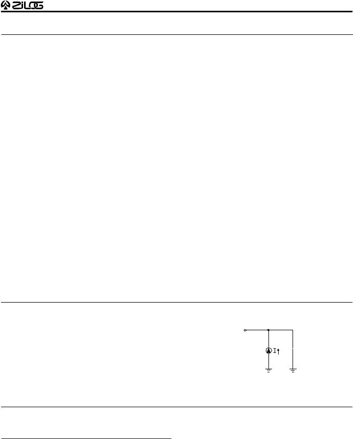
STANDARD TEST CONDITIONS
The characteristics listed below apply for standard test conditions as noted. All voltages are referenced to Ground. Positive current flows into the referenced pin (Figure 6).
From Output
Under Test
 150 pF
Figure 6. Test Load Diagram
CAPACITANCE
TA = 25°C, VCC = GND = 0V, f = 1.0 MHz, unmeasured pins returned to GND.
Parameter |
Min |
Max |
|
|
|
|
|
|
|
Input capacitance |
0 |
15 pF |
|
|
Output capacitance |
0 |
20 pF |
|
|
I/O capacitance |
0 |
25 pF |
|
|
|
|
|
|
|
|
|
|
|
|
DS96DZ80301 (11/96) |
|
P R E L I M I N A R Y |
1-5 |
|

Z86C02/E02/L02
Low-Cost, 512-Byte ROM Microcontrollers
DC ELECTRICAL CHARACTERISTICS
Z86C02
|
|
|
TA = 40°C to +105°C |
|
|
|
|
|
|
|
|
TA = 0°C to +70°C |
Typical |
|
|
|
|
Sym. |
Parameter |
VCC [4] |
Min |
Max |
@ 25°C |
Units |
Conditions |
Notes |
VCH |
Clock Input High |
3.0V |
0.8 VCC |
VCC+0.3 |
1.7 |
V |
Driven by External |
|
|
Voltage |
|
|
|
|
|
Clock Generator |
|
|
|
|
|
|
|
|
|
|
|
|
5.5V |
0.8 VCC |
VCC+0.3 |
2.8 |
V |
Driven by External |
|
|
|
|
|
|
|
|
Clock Generator |
|
|
|
|
|
|
|
|
|
|
VCL |
Clock Input Low |
3.0V |
VSS–0.3 |
0.2 VCC |
0.8 |
V |
Driven by External |
|
|
Voltage |
|
|
|
|
|
Clock Generator |
|
|
|
5.5V |
VSS–0.3 |
0.2 VCC |
1.7 |
V |
Driven by External |
|
|
|
|
|
|
|
|
Clock Generator |
|
|
|
|
|
|
|
|
|
|
VIH |
Input High Voltage |
3.0V |
0.7 VCC |
VCC+0.3 |
1.8 |
V |
|
[1] |
|
|
5.5V |
0.7 VCC |
VCC+0.3 |
2.8 |
V |
|
[1] |
VIL |
Input Low Voltage |
3.0V |
VSS–0.3 |
0.2 VCC |
0.8 |
V |
|
[1] |
|
|
5.5V |
VSS–0.3 |
0.2 VCC |
1.5 |
V |
|
[1] |
VOH |
Output High Voltage |
3.0V |
VCC–0.4 |
|
3.0 |
V |
IOH = –2.0 mA |
[5] |
|
|
5.5V |
VCC–0.4 |
|
4.8 |
V |
IOH = –2.0 mA |
[5] |
|
|
3.0V |
VCC–0.4 |
|
3.0 |
V |
Low Noise @ |
|
|
|
|
|
|
|
|
IOH = –0.5 mA |
|
|
|
5.5V |
VCC–0.4 |
|
4.8 |
V |
Low Noise @ |
|
|
|
|
|
|
|
|
IOH = –0.5 mA |
|
VOL1 |
Output Low Voltage |
3.0V |
|
0.8 |
0.2 |
V |
IOL = +4.0 mA |
[5] |
|
|
5.5V |
|
0.4 |
0.1 |
V |
IOL = +4.0 mA |
[5] |
|
|
3.0V |
|
0.8 |
0.2 |
V |
Low Noise @ |
|
|
|
|
|
|
|
|
IOL = 1.0 mA |
|
|
|
5.5V |
|
0.4 |
0.1 |
V |
Low Noise @ |
|
|
|
|
|
|
|
|
IOL = 1.0 mA |
|
VOL2 |
Output Low Voltage |
3.0V |
|
1.0 |
0.8 |
V |
IOL = +12 mA |
[5] |
|
|
5.5V |
|
0.8 |
0.3 |
V |
IOL = +12 mA |
[5] |
VOFFSET |
Comparator Input |
3.0V |
|
25 |
10 |
mV |
|
|
|
Offset Voltage |
5.5V |
|
25 |
10 |
mV |
|
|
|
|
|
|
|
|
|
|
|
VLV |
VCC Low Voltage |
|
|
|
|
V |
|
|
|
Auto Reset |
|
2.2 |
2.8 |
2.6 |
V |
|
[9] |
|
|
|
|
|
|
|
|
|
|
|
|
2.0 |
3.0 |
2.6 |
V |
|
[10] |
|
|
|
|
|
|
|
|
|
IIL |
Input Leakage |
3.0V |
–1.0 |
1.0 |
|
A |
VIN = 0V, VCC |
|
|
(Input Bias Current |
|
|
|
|
|
|
|
|
5.5V |
–1.0 |
1.0 |
|
A |
VIN = 0V, VCC |
|
|
|
of Comparator) |
|
|
|||||
|
|
|
|
|
|
|
|
|
|
|
|
|
|
|
|
|
|
IOL |
Output Leakage |
3.0V |
–1.0 |
1.0 |
|
A |
VIN = 0V, VCC |
|
|
|
5.5V |
–1.0 |
1.0 |
|
A |
VIN = 0V, VCC |
|
VVICR |
Comparator Input |
|
VSS–0.3 |
VCC –1.0 |
|
V |
|
[9] |
|
Common Mode |
|
|
|
|
|
|
|
|
|
VSS–0.3 |
VCC –1.5 |
|
V |
|
[10] |
|
|
Voltage Range |
|
|
|
||||
|
|
|
|
|
|
|
|
|
|
|
|
|
|
|
|
|
|
1-6 |
P R E L I M I N A R Y |
DS96DZ80301 (11/96) |

Z86C02/E02/L02
Low-Cost, 512-Byte ROM Microcontrollers
DC CHARACTERISTICS
Z86C02
|
|
|
TA = 40°C to+105°C |
|
|
|
|
|
|
|
VCC [4] |
TA = 0°C to +70°C |
Typical |
|
|
|
|
Sym. Parameter |
Min |
Max |
@ 25°C |
Units |
Conditions |
Notes |
||
|
|
|
|
|
|
|
|
|
ICC |
Supply Current |
3.0V |
|
3.5 |
1.5 |
mA |
@ 2 MHz |
[5,6,7] |
|
|
5.5V |
|
7.0 |
3.8 |
mA |
@ 2 MHz |
[5,6,7] |
|
|
|
|
|
|
|
|
|
|
|
3.0V |
|
8.0 |
3.0 |
mA |
@ 8 MHz |
[5,6,7] |
|
|
|
|
|
|
|
|
|
|
|
5.5V |
|
11.0 |
4.4 |
mA |
@ 8 MHz |
[5,6,7] |
|
|
|
|
|
|
|
|
|
ICC1 |
Standby Current (Halt Mode) |
3.0V |
|
2.5 |
0.7 |
mA |
@ 2 MHz |
[5,6,7] |
|
|
5.5V |
|
4.0 |
2.5 |
mA |
@ 2 MHz |
[5,6,7] |
|
|
|
|
|
|
|
|
|
|
|
3.0V |
|
4.0 |
1.0 |
mA |
@ 8 MHz |
[5,6,7] |
|
|
|
|
|
|
|
|
|
|
|
5.5V |
|
5.0 |
3.0 |
mA |
@ 8 MHz |
[5,6,7] |
|
|
|
|
|
|
|
|
|
ICC |
Supply Current (Low Noise Mode) |
3.0V |
|
3.5 |
1.5 |
mA |
@ 1 MHz |
[5,6,7] |
|
|
5.5V |
|
7.0 |
3.8 |
mA |
@ 1 MHz |
[5,6,7] |
|
|
|
|
|
|
|
|
|
|
|
3.0V |
|
5.8 |
2.5 |
mA |
@ 2 MHz |
[5,6,7] |
|
|
|
|
|
|
|
|
|
|
|
5.5V |
|
9.0 |
4.0 |
mA |
@ 2 MHz |
[5,6,7] |
|
|
|
|
|
|
|
|
|
|
|
3.0V |
|
8.0 |
3.0 |
mA |
@ 4 MHz |
[5,6,7] |
|
|
|
|
|
|
|
|
|
|
|
5.5V |
|
11.0 |
4.4 |
mA |
@ 4 MHz |
[5,6,7] |
|
|
|
|
|
|
|
|
|
ICC1 |
Standby Current |
3.0V |
|
2.5 |
0.7 |
mA |
@ 1 MHz |
[6,7,8] |
|
(Low Noise Halt Mode) |
5.5V |
|
4.0 |
2.5 |
mA |
@ 1 MHz |
[6,7,8] |
|
|
|
|
|
|
|
|
|
|
|
3.0V |
|
3.0 |
0.9 |
mA |
@ 2 MHz |
[6,7,8] |
|
|
|
|
|
|
|
|
|
|
|
5.5V |
|
4.5 |
2.8 |
mA |
@ 2 MHz |
[6,7,8] |
|
|
|
|
|
|
|
|
|
|
|
3.0V |
|
4.0 |
1.0 |
mA |
@ 4 MHz |
[6,7,8] |
|
|
|
|
|
|
|
|
|
|
|
5.5V |
|
5.0 |
3.0 |
mA |
@ 4 MHz |
[6,7,8] |
|
|
|
|
|
|
|
|
|
ICC2 |
Standby Current (Stop Mode) |
3.0V |
|
10 |
1.0 |
A |
|
[6,7,8,9] |
|
|
3.0V |
|
20 |
1.0 |
A |
|
[6,7,8,10] |
|
|
|
|
|
|
|
|
|
|
|
5.5V |
|
10 |
1.0 |
A |
|
[6,7,8,9] |
|
|
|
|
|
|
|
|
|
|
|
5.5V |
|
20 |
1.0 |
A |
|
[6,7,8,10] |
|
|
|
|
|
|
|
|
|
IALL |
Auto Latch Low Current |
3.0V |
|
12 |
3.0 |
A |
0V < VIN < VCC |
|
|
|
5.5V |
|
32 |
16 |
A |
0V < VIN < VCC |
|
IALH |
Auto Latch High Current |
3.0V |
|
–8 |
-1.5 |
A |
0V < VIN < VCC |
|
|
|
5.5V |
|
–16 |
-8.0 |
A |
0V < VIN < VCC |
|
Notes:
1.ort 0, 2, and 3 only.
2.VSS = 0V = GND.
3.The device operates down to VLV The minimum operational VCC is determined on the value of the voltage VLV at the ambient temperature.
4.VCC = 3.0V to 5.5V, typical values measured at VCC = 3.3V and VCC = 5.0V.
5.Standard mode (not Low EMI mode).
6.Inputs at VCC or VSS, outputs unloaded.
7.Halt mode and Low EMI mode.
8.WDT not running.
9.TA= 0˚C to 70˚C.
10.TA= 40˚C to 105˚C.
DS96DZ80301 (11/96) |
P R E L I M I N A R Y |
1-7 |

Z86C02/E02/L02
Low-Cost, 512-Byte ROM Microcontrollers
DC CHARACTERISTICS
Z86L02
|
|
VCC [4] |
TA = 0°C to +70°C |
Typical |
|
|
|
|
Sym. |
Parameter |
Min |
Max |
@ 25°C |
Units |
Conditions |
Notes |
|
VCH |
Clock Input High |
2.0V |
0.9 VCC |
VCC+0.3 |
|
V |
Driven by External |
|
|
Voltage |
|
|
|
|
|
Clock Generator |
|
|
|
|
|
|
|
|
|
|
|
|
3.9V |
0.9 VCC |
VCC+0.3 |
|
V |
Driven by External |
|
|
|
|
|
|
|
|
Clock Generator |
|
VCL |
Clock Input Low |
2.0V |
VSS–0.3 |
0.1 VCC |
|
V |
Driven by External |
|
|
Voltage |
|
|
|
|
|
Clock Generator |
|
|
|
|
|
|
|
|
|
|
|
|
3.9V |
VSS–0.3 |
0.1 VCC |
|
V |
Driven by External |
|
|
|
|
|
|
|
|
Clock Generator |
|
|
|
|
|
|
|
|
|
|
VIH |
Input High Voltage |
2.0V |
0.9 VCC |
VCC+0.3 |
|
V |
|
[1] |
|
|
3.9V |
0.9 VCC |
VCC+0.3 |
|
V |
|
[1] |
VIL |
Input Low Voltage |
2.0V |
VSS–0.3 |
0.1 VCC |
|
V |
|
[1] |
|
|
3.9V |
VSS–0.3 |
0.1 VCC |
|
V |
|
[1] |
VOH |
Output High Voltage |
2.0V |
VCC–0.4 |
|
3.0 |
V |
IOH = – 500 A |
[5] |
|
|
3.9V |
VCC–0.4 |
|
3.0 |
V |
IOH = –500 A |
[5] |
VOL1 |
Output Low Voltage |
2.0V |
|
0.8 |
0.2 |
V |
IOL = +1.0 mA |
[5] |
|
|
3.9V |
|
0.4 |
0.1 |
V |
IOL = +1.0 mA |
[5] |
VOL2 |
Output Low Voltage |
2.0V |
|
1.0 |
0.8 |
V |
IOL = + 3.0 mA |
[5] |
|
|
3.9V |
|
0.8 |
0.3 |
V |
IOL = + 3.0 mA |
[5] |
VOFFSET |
Comparator Input |
2.0V |
|
25 |
10 |
mV |
|
|
|
Offset Voltage |
3.9V |
|
25 |
10 |
mV |
|
|
|
|
|
|
|
|
|
|
|
VLV |
VCC Low Voltage |
|
1.4 |
2.15 |
|
V |
|
|
|
Auto Reset |
|
|
|
|
|
|
|
|
|
|
|
|
|
|
|
|
IIL |
Input Leakage |
2.0V |
–1.0 |
1.0 |
|
A |
VIN = 0V, VCC |
|
|
(Input Bias Current |
|
|
|
|
|
|
|
|
3.9V |
–1.0 |
1.0 |
|
A |
VIN = 0V, VCC |
|
|
|
of Comparator) |
|
|
|||||
|
|
|
|
|
|
|
|
|
|
|
|
|
|
|
|
|
|
IOL |
Output Leakage |
2.0V |
–1.0 |
1.0 |
|
A |
VIN = 0V, VCC |
|
|
|
3.9V |
–1.0 |
1.0 |
|
A |
VIN = 0V, VCC |
|
VVICR |
Comparator Input |
|
VSS –0.3 |
VCC –1.0 |
|
V |
|
|
|
Common Mode |
|
|
|
|
|
|
|
Voltage Range
1-8 |
P R E L I M I N A R Y |
DS96DZ80301 (11/96) |

Z86C02/E02/L02
Low-Cost, 512-Byte ROM Microcontrollers
|
|
VCC [4] |
TA = 0°C to +70°C |
Typical |
|
|
|
|
Sym |
Parameter |
Min |
Max |
@ 25°C |
Units |
Conditions |
Notes |
|
|
|
|
|
|
|
|
|
|
ICC |
Supply Current |
2.0V |
|
3.3 |
|
mA |
@ 2 MHz |
[5,6] |
|
|
3.9V |
|
6.8 |
|
mA |
@ 2 MHz |
[5,6] |
|
|
|
|
|
|
|
|
|
|
|
2.0V |
|
6.0 |
|
mA |
@ 8 MHz |
[5,6] |
|
|
|
|
|
|
|
|
|
|
|
3.9V |
|
9.0 |
|
mA |
@ 8 MHz |
[5,6] |
|
|
|
|
|
|
|
|
|
ICC1 |
Standby Current (Halt Mode) |
2.0V |
|
2.3 |
|
mA |
@ 2 MHz |
[5,6,7] |
|
|
3.9V |
|
3.8 |
|
mA |
@ 2 MHz |
[5,6,7] |
|
|
|
|
|
|
|
|
|
|
|
2.0V |
|
3.8 |
|
mA |
@ 8 MHz |
[5,6,7] |
|
|
|
|
|
|
|
|
|
|
|
3.9V |
|
4.8 |
|
mA |
@ 8 MHz |
[5,6,7] |
|
|
|
|
|
|
|
|
|
ICC2 |
Standby Current (Stop Mode) |
2.0V |
|
10 |
1.0 |
A |
|
[6,7] |
|
|
3.9V |
|
10 |
1.0 |
A |
|
[6,7] |
|
|
|
|
|
|
|
|
|
IALL |
Auto Latch Low Current |
2.0V |
|
12 |
3.0 |
A |
0V < VIN < VCC |
|
|
|
3.9V |
|
32 |
16 |
A |
0V < VIN < VCC |
|
IALH |
Auto Latch High Current |
2.0V |
|
–8 |
-1.5 |
A |
0V < VIN < VCC |
|
|
|
3.9V |
|
–16 |
-8.0 |
A |
|
|
|
|
|
|
|
|
|
|
|
Notes:
1.Port 0, 2, and 3 only
2.VSS = 0V = GND.The device operates down to VLV. The minimum operational VCC is determined by the value of the voltage VLV at the ambient temperature.
3.VCC = 2.0V to 3.9V, typical values measured at VCC = 3.3 V.
4.Standard Mode (not Low EMI mode).
5.Inputs at VCC or VSS, outputs are unloaded.
6.WDT is not running.
DS96DZ80301 (11/96) |
P R E L I M I N A R Y |
1-9 |

Z86C02/E02/L02
Low-Cost, 512-Byte ROM Microcontrollers
DC CHARACTERISTICS
Z86E02
|
|
|
TA = –40°C to +105°C |
|
|
|
|
|
|
|
VCC [4] |
TA = 0°C to +70°C |
Typical |
|
|
|
|
Sym. |
Parameter |
Min |
Max |
@ 25°C |
Units |
Conditions |
Notes |
|
|
|
|
|
|
|
|
|
|
VCH |
Clock Input High |
4.5V |
0.8 VCC |
VCC+0.3 |
2.8 |
V |
Driven by External |
|
|
Voltage |
|
|
|
|
|
Clock Generator |
|
|
|
5.5V |
0.8 VCC |
VCC+0.3 |
2.8 |
V |
Driven by External |
|
|
|
|
|
|
|
|
Clock Generator |
|
VCL |
Clock Input Low |
4.5V |
VSS–0.3 |
0.2 VCC |
1.7 |
V |
Driven by External |
|
|
Voltage |
|
|
|
|
|
Clock Generator |
|
|
|
|
|
|
|
|
|
|
|
|
5.5V |
VSS–0.3 |
0.2 VCC |
1.7 |
V |
Driven by External |
|
|
|
|
|
|
|
|
Clock Generator |
|
|
|
|
|
|
|
|
|
|
VIH |
Input High Voltage |
4.5V |
0.7 VCC |
VCC+0.3 |
2.8 |
V |
|
|
|
|
5.5V |
0.7 VCC |
VCC+0.3 |
2.8 |
V |
|
|
VIL |
Input Low Voltage |
4.5V |
VSS–0.3 |
0.2 VCC |
1.5 |
V |
|
|
|
|
5.5V |
VSS–0.3 |
0.2 VCC |
1.5 |
V |
|
|
VOH |
Output High Voltage |
4.5V |
VCC–0.4 |
|
4.8 |
V |
IOH = –2.0 mA |
[5] |
|
|
5.5V |
VCC–0.4 |
|
4.8 |
V |
IOH = –2.0 mA |
[5] |
|
|
4.5V |
VCC–0.4 |
|
4.8 |
V |
Low Noise @ |
|
|
|
|
|
|
|
|
IOH = –0.5 mA |
|
|
|
5.5V |
VCC–0.4 |
|
4.8 |
V |
|
|
VOL1 |
Output Low Voltage |
4.5V |
|
0.4 |
0.1 |
V |
IOL = +4.0 mA |
[5] |
|
|
5.5V |
|
0.4 |
0.1 |
V |
IOL = +4.0 mA |
[5] |
|
|
4.5V |
|
0.4 |
0.1 |
V |
Low Noise @ |
|
|
|
|
|
|
|
|
IOL = 1.0 mA |
|
|
|
5.5V |
|
0.4 |
0.1 |
V |
Low Noise @ |
|
|
|
|
|
|
|
|
IOL = 1.0 mA |
|
VOL2 |
Output Low Voltage |
4.5V |
|
1.0 |
0.8 |
V |
IOL = +12 mA |
[5] |
|
|
5.5V |
|
1.0 |
0.8 |
V |
IOL = +12 mA |
[5] |
VOFFSET |
Comparator Input |
4.5V |
|
25 |
10 |
mV |
|
|
|
Offset Voltage |
5.5V |
|
25 |
10 |
mV |
|
|
|
|
|
|
|
|
|
|
|
VLV |
VCC Low Voltage |
|
2.6 |
3.3 |
3.0 |
V |
|
[9] |
|
Auto Reset |
|
2.2 |
3.6 |
3.0 |
V |
|
[10] |
|
|
|
|
|
|
|
|
|
IIL |
Input Leakage (Input |
4.5V |
–1.0 |
1.0 |
|
A |
VIN = 0V, VCC |
|
|
Bias Current of |
|
|
|
|
|
|
|
|
5.5V |
–1.0 |
1.0 |
|
A |
VIN = 0V, VCC |
|
|
|
Comparator) |
|
|
|||||
|
|
|
|
|
|
|
|
|
|
|
|
|
|
|
|
|
|
IOL |
Output Leakage |
4.5V |
–1.0 |
1.0 |
|
A |
VIN = 0V, VCC |
|
|
|
5.5V |
–1.0 |
1.0 |
|
A |
VIN = 0V, VCC |
|
VVICR |
Comparator Input |
|
VSS–0.3 |
VCC –1.0 |
|
V |
|
[9] |
|
Common Mode |
|
|
|
|
|
|
|
|
|
|
|
|
|
|
|
|
|
Voltage Range |
|
|
|
|
|
|
|
|
|
VSS–0.3 |
VCC –1.5 |
|
V |
|
[10] |
|
|
|
|
|
|
||||
1-10 |
P R E L I M I N A R Y |
DS96DZ80301 (11/96) |
Z86C02/E02/L02
Low-Cost, 512-Byte ROM Microcontrollers
|
|
|
TA = –40°C to +105°C |
|
|
|
|
|
|
|
|
TA = 0°C to +70°C |
Typical |
|
|
|
|
Sym. Parameter |
VCC [4] |
Min |
Max |
@ 25°C |
Units |
Conditions |
Notes |
|
ICC |
Supply Current |
4.5V |
|
9.0 |
3.8 |
mA |
@ 2 MHz |
[5,6] |
|
|
5.5V |
|
9.0 |
3.8 |
mA |
@ 2 MHz |
[5,6] |
|
|
|
|
|
|
|
|
|
|
|
4.5V |
|
15.0 |
4.4 |
mA |
@ 8 MHz |
[5,6] |
|
|
|
|
|
|
|
|
|
|
|
5.5V |
|
15.0 |
4.4 |
mA |
@ 1 MHz |
[5,6] |
|
|
|
|
|
|
|
|
|
ICC1 |
Standby Current (HALT mode) |
4.5V |
|
4.0 |
2.5 |
mA |
@ 2 MHz |
[5,6] |
|
|
5.5V |
|
4.0 |
2.5 |
mA |
@ 2 MHz |
[5,6] |
|
|
|
|
|
|
|
|
|
|
|
4.5V |
|
5.0 |
3.0 |
mA |
@ 4 MHz |
[5,6] |
|
|
|
|
|
|
|
|
|
|
|
5.5V |
|
5.0 |
3.0 |
mA |
@ 4 MHz |
[5,6] |
|
|
|
|
|
|
|
|
|
ICC |
Supply Current (Low Noise |
4.5V |
|
9.0 |
3.8 |
mA |
|
[6] |
|
Mode) |
5.5V |
|
9.0 |
3.8 |
mA |
|
[6] |
|
|
|
|
|
|
|
|
|
|
|
4.5V |
|
11.0 |
4.0 |
mA |
@ 2 MHz |
[6] |
|
|
|
|
|
|
|
|
|
|
|
5.5V |
|
11.0 |
4.0 |
mA |
@ 2 MHz |
[6] |
|
|
|
|
|
|
|
|
|
|
|
4.5V |
|
15.0 |
4.4 |
mA |
@ 4 MHz |
[6] |
|
|
|
|
|
|
|
|
|
|
|
5.5V |
|
15.0 |
4.4 |
mA |
@ 4 MHz |
[6] |
|
|
|
|
|
|
|
|
|
ICC1 |
Standby Current (Low Noise |
4.5V |
|
4.0 |
2.5 |
mA |
@ 1 MHz |
[6,7,8] |
|
Halt Mode) |
5.5V |
|
4.0 |
2.5 |
mA |
@ 1 MHz |
[6,7,8] |
|
|
|
|
|
|
|
|
|
|
|
4.5V |
|
4.5 |
2.7 |
mA |
@ 2 MHz |
[6,7,8] |
|
|
|
|
|
|
|
|
|
|
|
5.5V |
|
4.5 |
2.7 |
mA |
@ 2 MHz |
[6,7,8] |
|
|
|
|
|
|
|
|
|
|
|
4.5V |
|
5.0 |
3.0 |
mA |
@ 4 MHz |
[6,7,8] |
|
|
|
|
|
|
|
|
|
|
|
5.5V |
|
5.0 |
3.0 |
mA |
@ 4 MHz |
[6,7,8] |
|
|
|
|
|
|
|
|
|
ICC2 |
Standby Current (Stop Mode) |
4.5V |
|
10 |
1.0 |
A |
|
[6,7,9] |
|
|
4.5V |
|
20 |
1.0 |
A |
|
[6,7,10] |
|
|
|
|
|
|
|
|
|
|
|
5.5V |
|
10 |
1.0 |
A |
|
[6,7,9] |
|
|
|
|
|
|
|
|
|
|
|
5.5V |
|
20 |
1.0 |
A |
|
6,7,10] |
|
|
|
|
|
|
|
|
|
IALL |
Auto Latch Low Current |
4.5V |
|
32 |
16 |
A |
0V <VIN<VCC |
|
|
|
5.5V |
|
32 |
16 |
A |
0V <VIN<VCC |
|
ALH |
Auto Latch High |
4.5V |
|
–16 |
-8.0 |
A |
0V <VIN<VCC |
|
|
|
5.5V |
|
–16 |
–8.0 |
A |
0V <VIN<VCC |
|
Notes:
1.Port 0, 2, and 3 only.
2.VSS = 0V = GND.
3.The device operates down to VLV of the specified frequency for VLV. The minimum operational VCC is determined by the value of the voltage VLV at the ambient temperature.
4.The VLV increases as the temperature decreases.
5.VCC = 4.5V to 5.5V, typical values measured at VCC = 5.0V.
6.Standard mode (not Low EMI mode).
7.Inputs at VCC or VSS, outputs unloaded.
8.WDT not running.
9.Halt mode and Low EMI mode.
10.TA= 0˚C to 70˚C.TA= –40˚C to 105˚C.
DS96DZ80301 (11/96) |
P R E L I M I N A R Y |
1-11 |
 Loading...