


Z86C6116FSC
ZILOG Z86C6116FSC, Z86C6116PEC, Z86C6116PSC, Z86C6116VEC, Z86C6116VSC Datasheet
...
1
Z86C61/62/96
Z8
®
MICROCONTROLLER
P
RODUCT
S
PECIFICATION
Z86C61/62/96
CMOS Z8
®
MICROCONTROLLER
FEATURES
■ 8-Bit CMOS Microcontroller
■ 40-Pin DIP, 44-Pin PLCC, 64-Pin DIP, or
68-Pin PLCC Package
■ 32 Input/Output Lines (Z86C61 Only)
■ 52 Input/Output Lines (Z86C62 and Z86C96)
■ 3.0V to 5.5V Operating Range
■ Low Power Consumption: 200 mW (max)
■ Fast Instruction Pointer: 0.75 µs @ 16 MHz
■ Two Standby Modes: STOP and HALT
■ Full-Duplex UART
■ All Digital Inputs are TTL Levels
GENERAL DESCRIPTION
The Z86C61/62/96 microcontroller is a member of the Z8
single-chip microcontroller family with 16 Kbytes of ROM
and 256 bytes of RAM. The Z86C96 is ROMless.
The Z86C61 is offered in 40-pin DIP and 44-pin PLCC style
packages, however, the ROMless pin option is available
on the 44-pin version only. The Z86C62/96 is offered in 64-
pin DIP and 68-pin PLCC style packages. A ROMless pin
option enables these MCUs to address both external
memory and preprogrammed ROM, making them well-
suited for high-volume applications or where code flexibil-
ity is required.
With 16 Kbytes of ROM and 256 bytes of general-purpose
RAM, these low-cost, low power consumption CMOS
Z86C61/62/96 MCUs offer fast execution, efficient use of
memory, sophisticated interrupts, input/output bit manipu-
lation capabilities, and easy hardware/software system
expansion.
The Z86C61/62/96 architecture is characterized by Zilog’s
8-bit microcontroller core. The device offers a flexible I/O
scheme, an efficient register and address space structure,
multiplexed capabilities between address/data, I/O, and a
number of ancillary features that are useful in many indus-
trial and advanced scientific applications.
For applications which demand powerful I/O capabilities,
the Z86C61 fulfills this with 32 pins dedicated to input and
output. These lines are grouped into four ports with eight
lines each. The Z86C62/96 has 52 pins for input and
output, and these lines are grouped into six, 8-bit ports and
one 4-bit port. Each port is configurable under software
control to provide timing, status signals, serial or parallel
I/O with or without handshake, and an address/data bus
for interfacing external memory.
■ Auto Latches
■ RAM and ROM Protect
■ 16 Kbytes of ROM
■ 256 Bytes of RAM
■ Two Programmable 8-Bit Counter/Timers,
Each with 6-Bit Programmable Prescaler
■ Six Vectored, Priority Interrupts from Eight
Different Sources
■ Clock Speeds: 16 and 20 MHz
■ On-Chip Oscillator that Accepts a Crystal,
Ceramic Resonator, LC, or External Clock Drive
2
Z86C61/62/96
Z8
®
MICROCONTROLLER
GENERAL DESCRIPTION (Continued)
There are three basic address spaces available to support
this configuration: Program Memory, Data Memory, and
236 General-Purpose Registers.
To unburden the program from coping with the real-time
tasks, such as counting/timing and serial data communi-
cation, the Z86C61/62/96 offers two on-chip counter/tim-
ers with a large number of user selectable modes, and an
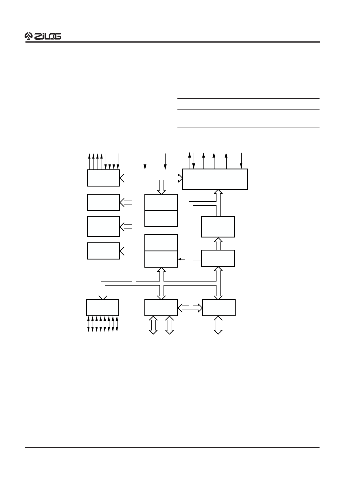
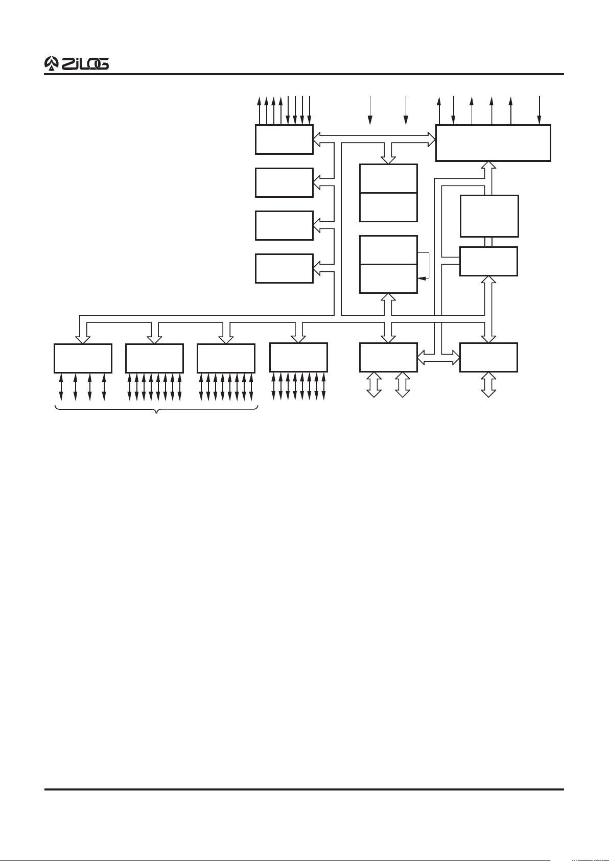
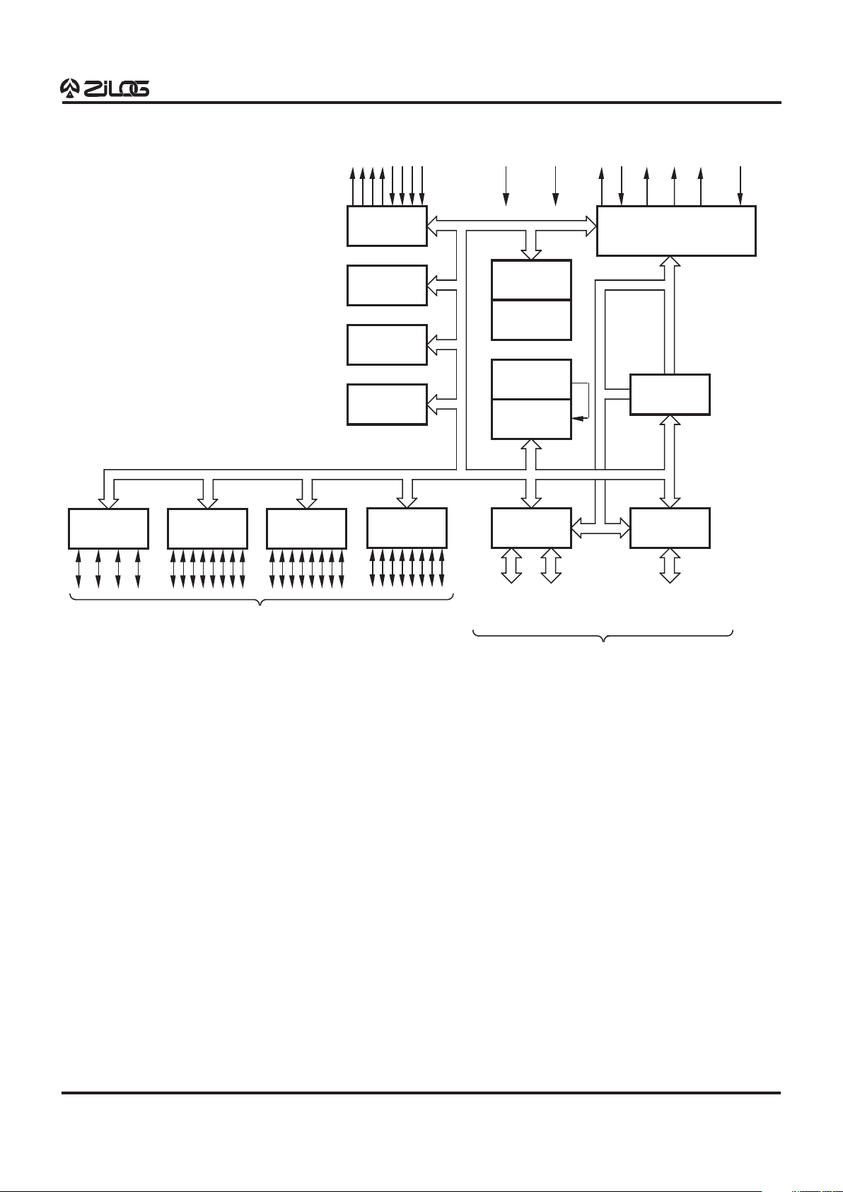
on-board UART (Figures 1, 2, and 3).
Notes:
All Signals with a preceding front slash, "/", are active Low, e.g.,
B//W (WORD is active Low); /B/W (BYTE is active Low, only).
Power connections follow conventional descriptions below:
Connection Circuit Device
Power V
CC
V
DD
Ground GND V
SS
Port 3
UART
Counter/
Timers
(2)
Interrupt
Control
Port 2
I/O
(Bit Programmable)
ALU
FLAGS
Register
Pointer
Register File
256 x 8-Bit
Machine Timing and
Instruction Control
Prg. Memory
16,384
x 8-Bit
Program
Counter
Vcc GND
XTAL
44
Port 0
Output Input
Address or I/O
(Nibble Programmable)
Port 1
8
Address/Data or I/O
(Byte Programmable)
/AS /DS R//W /RESET
Figure 1. Z86C61 Functional Block Diagram
3
Z86C61/62/96
Z8
®
MICROCONTROLLER
Port 3
Counter/
Timers (2)
Interrupt
Control
Port 2
ALU
Flags
Register
Pointer
Register File
256 x 8-Bit
Machine Timing and
Instruction Control
Program
Counter
Vcc GND XTAL R//W /RESETOutput Input
UART
Port 0 Port 1
Address or I/O
(Nibble Programmable)
Address/Data or I/O
(Byte Programmable)
44 8
/AS /DS
Port 4Port 5Port 6
I/O
(Bit Programmable)
I/O
(Bit Programmable)
Program
Memory
16,384 x 8-Bit
Figure 2. Z86C62 Functional Block Diagram
4
Z86C61/62/96
Z8
®
MICROCONTROLLER
GENERAL DESCRIPTION (Continued)
Port 3
Counter/
Timers (2)
Interrupt
Control
Port 2
ALU
Flags
Register
Pointer
Register File
256 x 8-Bit
Machine Timing and
Instruction Control
Program
Counter
Vcc GND XTAL R//W /RESETOutput Input
UART
Port 0 Port 1
Address or I/O
(Nibble Programmable)
Address/Data or I/O
(Byte Programmable)
44 8
/AS /DS
Z-BUS When Used
As Address/Data Bus
Port 4Port 5Port 6
I/O
(Bit Programmable)
Figure 3. Z86C96 Functional Block Diagram

5
Z86C61/62/96
Z8
®
MICROCONTROLLER
PIN DESCRIPTION
Table 1. Z86C61 40-Pin DIP Pin Identification
Pin # Symbol Function Direction
1V
CC
Power Supply Input
2 XTAL2 Crystal, Oscillator Clock Output
3 XTAL1 Crystal, Oscillator Clock Input
4 P37 Port 3, Pin 7 Output
5 P30 Port 3, Pin 0 Input
6 /RESET Reset Input
7 R//W Read/Write Output
8 /DS Data Strobe Output
9 /AS Address Strobe Output
10 P35 Port 3, Pin 5 Output
11 GND Ground Input
12 P32 Port 3, Pin 2 Input
13-20 P07-P00 Port 0, Pins 0,1,2,3,4,5,6,7 In/Output
21-28 P17-P10 Port 1, Pins 0,1,2,3,4,5,6,7 In/Output
29 P34 Port 3, Pin 4 Output
30 P33 Port 3, Pin 3 Input
31-38 P27-P20 Port 2, Pins 0,1,2,3,4,5,6,7 In/Output
39 P31 Port 3, Pin 1 Input
40 P36 Port 3, Pin 6 Output
1
2
9
3
4
5
6
7
8
40
39
38
37
36
35
34
33
32
P36
P31
P21
P27
P26
P25
P24
P23
P22
VCC
XTAL2
P37
P30
/RESE
T
R//W
/DS
31
30
29
28
2714
10
11
12
13
XTAL1
GND
P32
P00
P01
P20
P33
P34
P17
P16
Z86C61
DIP
15
26
25
24
23
22
21
20
16
17
18
19
/AS
P35
P02
P03
P06
P07
P05
P04 P13
P15
P14
P12
P11
P10
Figure 4. Z86C61 40-Pin DIP
Pin Assignments
6
Z86C61/62/96
Z8
®
MICROCONTROLLER
PIN DESCRIPTION (Continued)
N/C
P30
P37
XTAL1
XTAL2
VCC
P36
P31
P27
P26
P25
P03
P04
P05
P06
P07
P10
P11
P12
P13
P14
N/C
N/C
P24
P23
P22
P21
P20
P33
P34
P17
P16
P15
/RESET
R//W
/DS
/AS
P35
GND
P32
P00
P01
P02
R//RL
7
8
9
10
11
12
13
14
15
16
17
38
37
36
35
34
33
32
31
30
29
39
Z86C61
PLCC
6543214443424140
18 19 20 21 22 23 24 25 26 27 28
Figure 5. Z86C61 44-Pin PLCC Pin Assignments
Pin # Symbol Function Direction
1V
CC
Power Supply Input
2 XTAL2 Crystal, Oscillator Clock Output
3 XTAL1 Crystal, Oscillator Clock Input
4 P37 Port 3, Pin 7 Output
5 P30 Port 3, Pin 0 Input
6 N/C Not Connected Input
7 /RESET Reset Input
8 R//W Read/Write Output
9 /DS Data Strobe Output
10 /AS Address Strobe Output
11 P35 Port 3, Pin 5 Output
12 GND Ground Input
13 P32 Port 3, Pin 2 Input
14-16 P02-P00 Port 0, Pins 0,1,2 In/Output
Pin # Symbol Function Direction
17 R//RL ROM/ROMless control Input
18-22 P07-P03 Port 0, Pins 3,4,5,6,7 In/Output
23-27 P14-P10 Port 1, Pins 0,1,2,3,4 In/Output
28 N/C Not Connected Input
29-31 P17-P15 Port 1, Pins 5,6,7 In/Output
32 P34 Port 3, Pin 4 Output
33 P33 Port 3, Pin 3 Input
34-38 P24-P20 Port 2, Pins 0,1,2,3,4 In/Output
39 N/C Not Connected Input
40-42 P25-P27 Port 2, Pins 5,6,7 In/Output
43 P31 Port 3, Pin 1 Input
44 P36 Port 3, Pin 6 Output
Table 2. Z86C61 44-Pin PLCC Pin Identification
7
Z86C61/62/96
Z8
®
MICROCONTROLLER
P44
VCC
P45
XTAL2
P47
/AS
P35
R//RL
GND
P32
P50
P51
P43
P42
P36
P31
P41
P40
P27
P26
P25
P24
P23
P22
P60
P61
P21
P20
GND
P33
P34
P62
XTAL1
P37
P30
N/C
/RESET
R//W
/DS
P46
1
2
3
4
5
6
7
8
9
10
11
12
13
14
15
16
17
18
19
20
63
62
61
60
59
58
57
56
55
54
53
52
51
50
49
48
47
46
45
44
Z86C62
DIP
P00
P01
P02
P03
P63
P17
P16
P15
21
22
23
24
43
42
41
40
P06
P07
VCC
P52
P53
P54
P14
P13
P12
P57
P56
P11
P10
P55
P04
P05
25
26
27
28
29
30
31
32
39
38
37
36
35
34
33
64
Figure 6. Z86C62 64-Pin DIP Pin Assignments
Table 3. Z86C62 64-Pin DIP Pin Identification
Pin # Symbol Function Direction
1 P44 Port 4, Pin 4 In/Output
2V
CC
Power Supply Input
3 P45 Port 4, Pin 5 In/Output
4 XTAL2 Crystal, Oscillator Clock Output
5 XTAL1 Crystal, Oscillator Clock Input
6 P37 Port 3, Pin 7 Output
7 P30 Port 3, Pin 0 Input
8 N/C Not Connected Input
9 /RESET Reset Input
10 R//W Read/Write Output
11 /DS Data Strobe Output
12-13 P47-P46 Port 4, Pin 6,7 In/Output
14 /AS Address Strobe Output
15 P35 Port 3, Pin 5 Output
16 R//RL ROM/ROMless control Input
17 GND Ground Input
18 P32 Port 3, Pin 2 Input
19-20 P51-P50 Port 5, Pin 0,1 In/Output
21-28 P07-P00 Port 0, Pins 0,1,2,3,4,5,6,7 In/Output
29 V
CC
Power Supply Input
30-33 P52-P55 Port 5, Pins 2,3,4,5 In/Output
34-35 P11-P10 Port 1, Pins 0,1 In/Output
36-37 P57-P56 Port 5, Pins 6,7 In/Output
38-43 P17-P12 Port 1, Pins 2,3,4,5,6,7 In/Output
44-45 P63-P62 Port 6, Pins 3,2 In/Output
46 P34 Port 3, Pin 4 Output
47 P33 Port 3, Pin 3 Input
48 GND Ground Input
49-50 P21-P20 Port 2, Pins 0,1 In/Output
51-52 P61-P60 Port 6, Pins 1,0 In/Output
53-58 P27-P22 Port 2, Pins 2,3,4,5,6,7 In/Output
59-60 P41-P40 Port 4, Pins 0,1 In/Output
61 P31 Port 3, Pin 1 Input
62 P36 Port 3, Pin 6 Output
63 P42 Port 4, Pin 2 In/Output
64 P43 Port 4, Pin 3 In/Output
8
Z86C61/62/96
Z8
®
MICROCONTROLLER
PIN DESCRIPTION (Continued)
Z86C62
PLCC
10
11
12
13
14
15
16
17
18
19
20
21
22
23
24
25
26
27 28 29 30 31 32 33 34 35 36 37 38 39 40 41 42 43
/Reset
P30
P37
XTAL1
XTAL2
P45
VCC
P44
P43
P42
P36
P31
P41
P40
P26
P25
P27
P54
VCC
P07
P14
P13
P12
P57
P56
P11
P10
P55
P53
P52
P06
P04
P03
P05
789 6543216867666564636261
60
59
58
57
56
55
54
53
52
51
50
49
48
47
46
45
44
P24
P23
P22
P60
P61
P21
P20
SCLK
/SYNC
GND
P33
P34
P62
P63
P17
P16
P15
R//W
/P0DS
/DS
P46
P47
/P1DS
/AS
/DTimers
P35
R//RL
GND
P32
P50
P51
P00
P01
P02
Figure 7. Z86C62 68-Pin PLCC Pin Assignments

9
Z86C61/62/96
Z8
®
MICROCONTROLLER
Table 4. Z86C62 68-Pin PLCC Pin Identification
Pin # Symbol Function Direction
1-2 P44-P43 Port 4, Pins 3,4 In/Output
3V
CC
Power Supply Input
4 P45 Port 4, Pin 5 In/Output
5 XTAL2 Crystal, Oscillator Clock Output
6 XTAL1 Crystal, Oscillator Clock Input
7 P37 Port 3, Pin 7 Output
8 P30 Port 3, Pin 0 Input
9 /RESET Reset Input
10 R//W Read/Write Output
11 /P0DS Port 0 Data Strobe Output
12 /DS Data Strobe Output
13-14 P47-P46 Port 4, Pins 6,7 In/Output
15 /P1DS Port 1, Data Strobe Output
16 /AS Address Strobe Output
17 /DTIMER DTIMER Input
18 P35 Port 3, Pin 5 Output
19 R//RL ROM/ROMless control Input
20 GND Ground Input
21 P32 Port 3, Pin 2 Input
22-23 P51-P50 Port 5, Pins 0,1 In/Output
Pin # Symbol Function Direction
24-31 P07-P00 Port 0, Pins 0,1,2,3,4,5,6,7 In/Output
32 V
CC
Power Supply Input
33-36 P55-P52 Port 5, Pins 2,3,4,5 In/Output
37-38 P11-P10 Port 1, Pins 0,1 In/Output
39-40 P56-P57 Port 5, Pins 6,7 In/Output
41-46 P17-P12 Port 1, Pins 2,3,4,5,6,7 In/Output
47-48 P63-P62 Port 6, Pins 3,2 In/Output
49 P34 Port 3, Pin 4 Output
50 P33 Port 3, Pin 3 Input
51 GND Ground Input
52 /SYNC Synchronization Output
53 SCLK System Clock Output
54-55 P21-P20 Port 2, Pins 0,1 In/Output
56-57 P60-P61 Port 6, Pins 1,0 In/Output
58-63 P27-P22 Port 2, Pins 2,3,4,5,6,7 In/Output
64-65 P41-P40 Port 4, Pins 0,1 In/Output
66 P31 Port 3, Pin 1 Input
67 P36 Port 3, Pin 6 Output
68 P42 Port 4, Pin 2 In/Output
10
Z86C61/62/96
Z8
®
MICROCONTROLLER
PIN DESCRIPTION (Continued)
Table 5. Z86C96 64-Pin DIP Pin Identification
Pin # Symbol Function Direction
1 P44 Port 4, Pin 4 In/Output
2V
CC
Power Supply Input
3 P45 Port 4, Pin 5 In/Output
4 XTAL2 Crystal, Oscillator Clock Output
5 XTAL1 Crystal, Oscillator Clock Input
6 P37 Port 3, Pin 7 Output
7 P30 Port 3, Pin 0 Input
8 N/C Not Connected Input
9 /RESET Reset Input
10 R//W Read/Write Output
11 /DS Data Strobe Output
12-13 P47-P46 Port 4, Pins 6,7 In/Output
14 /AS Address Strobe Output
15 P35 Port 3, Pin 5 Output
16 N/C Not Connected Input
17 GND Ground Input
18 P32 Port 3, Pin 2 Input
19-20 P51-P50 Port 5, Pins 0,1 In/Output
21-28 P07-P00 Port 0, Pins 0,1,2,3,4,5,6,7 In/Output
29 V
CC
Power Supply Input
30-33 P55-P52 Port 5, Pins 2,3,4,5 In/Output
34-35 P11-P10 Port 1, Pins 0,1 In/Output
36-37 P56-P57 Port 5, Pins 6,7 In/Output
38-43 P17-P12 Port 1, Pins 2,3,4,5,6,7 In/Output
44-45 P63-P62 Port 6, Pins 3,2 In/Output
46 P34 Port 3, Pin 4 Output
47 P33 Port 3, Pin 3 Input
48 GND Ground Input
49-50 P21-P20 Port 2, Pins 0,1 In/Output
51-52 P61-P60 Port 6, Pins 1,0 In/Output
53-58 P27-P22 Port 2, Pins 2,3,4,5,6,7 In/Output
59-60 P41-P40 Port 4, Pins 0,1 In/Output
61 P31 Port 3, Pin 1 Input
62 P36 Port 3, Pin 6 Output
63 P42 Port 4, Pin 2 In/Output
64 P43 Port 4, Pin 3 In/Output
Z86C96
DIP
P43
P42
P36
P31
P41
P40
P27
P26
P25
P24
P23
P22
P60
P61
P21
P20
GND
P33
P34
P62
63
62
61
60
59
58
57
56
55
54
53
52
51
50
49
48
47
46
45
44
P63
P17
P16
P15
43
42
41
40
P14
P13
P12
P57
P56
P11
P10
P55
39
38
37
36
35
34
33
64
P44
VCC
P45
XTAL2
P47
/AS
P35
N/C
GND
P32
P50
P51
XTAL1
P37
P30
NC
/RESET
R//W
/DS
P46
19
P00
P01
P02
P03
P06
P07
VCC
P52
P53
P54
P04
P05
1
2
3
4
5
6
7
8
9
20
21
22
23
24
25
26
27
28
29
30
31
32
10
11
12
13
14
15
16
17
18
Figure 8. Z86C96 64-Pin DIP Pin Assignments
11
Z86C61/62/96
Z8
®
MICROCONTROLLER
Z86C96
PLCC
789
654321
10
11
12
13
14
15
16
17
18
19
20
21
22
23
24
25
26
68 67 66 65 64 63 62 61
27 28 29 30 31 32 33 34 35 36 37 38 39 40 41 42 43
60
59
58
57
56
55
54
53
52
51
50
49
48
47
46
45
44
/RESET
P30
P37
XTAL1
XTAL2
P45
VCC
P44
P43
P42
P36
P31
P41
P40
P26
P25
P27
P54
VCC
P07
P14
P13
P12
P57
P56
P11
P10
P55
P53
P52
P06
P04
P03
P05
P24
P23
P22
P60
P61
P21
P20
SCLK
/SYNC
GND
P33
P34
P62
P63
P17
P16
P15
R//W
/P0DS
/DS
P46
P47
/P1DS
/AS
/DTimers
P35
N/C
GND
P32
P50
P51
P00
P01
P02
Figure 9. Z86C96 68-Pin PLCC Pin Assignments
12
Z86C61/62/96
Z8
®
MICROCONTROLLER
PIN DESCRIPTION (Continued)
Table 6. Z86C96 68-Pin PLCC Pin Identification
Pin # Symbol Function Direction
1-2 P44-P43 Port 4, Pins 3,4 In/Output
3V
CC
Power Supply Input
4 P45 Port 4, Pin 5 In/Output
5 XTAL2 Crystal, Oscillator Clock Output
6 XTAL1 Crystal, Oscillator Clock Input
7 P37 Port 3, Pin 7 Output
8 P30 Port 3, Pin 0 Input
9 /RESET Reset Input
10 R//W Read/Write Output
11 /P0DS Port 0 Data Strobe Output
12 /DS Data Strobe Output
13-14 P47-P46 Port 4, Pins 6,7 In/Output
15 /P1DS Port 1 Data Strobe Output
16 /AS Address Strobe Output
17 /DTIMER Disable Timers Input
18 P35 Port 3, Pin 5 Output
19 N/C Not Connected Input
20 GND Ground Input
21 P32 Port 3, Pin 2 Input
22-23 P51-P50 Port 5, Pins 0,1 In/Output
PIN FUNCTIONS
XTAL1, XTAL2
Crystal 1, Crystal 2
(time-based input and
output, respectively). These pins connect a parallel-
resonant crystal, ceramic resonator, LC, or any external
single-phase clock to the on-chip oscillator and buffer.
R//W (output, write Low). The Read/Write signal is Low
when the MCU is writing to the external program or data
memory.
/RESET (input, active Low). To avoid asynchronous and
noisy reset problems, the Z86C61/62/96 is equipped with
a reset filter of four external clocks (4TpC). If the external
/RESET signal is less than 4TpC in duration, no reset
occurs.
On the fifth clock after the /RESET is detected, an internal
RST signal is latched and held for an internal register count
of 18 external clocks, or for the duration of the external
/RESET, whichever is longer. During the reset cycle, /DS is
held active Low while /AS cycles at a rate of TpC/2. When
/RESET is deactivated, program execution begins at loca-
tion 000C (HEX). Reset time must be held Low for 50 ms,
or until V
CC
is stable, whichever is longer.
R//RL (input, active Low). This pin when connected to
GND disables the internal ROM and forces the device to
function as a Z86C96 ROMless Z8. (Note: When left
unconnected or pulled High to V
CC
the part functions as a
normal Z86C61/62 ROM version.) This pin is only available
on the 44-pin version of the Z86C61, and both versions of
the Z86C62.
/DS (output, active Low). Data Strobe is activated once for
each external memory transfer. For a READ operation,
data must be available prior to the trailing edge of /DS. For
WRITE operations, the falling edge of /DS indicates that
output data is valid.
/AS (output, active Low). Address Strobe is pulsed once
at the beginning of each machine cycle. Address out-
put is through Port 1 for all external programs. Memory
address transfers are valid at the trailing edge of /AS.
Under program control, /AS can be placed in the high-
impedance state along with Ports 0 and 1, Data Strobe,
and Read/Write.
Pin # Symbol Function Direction
24-31 P07-P00 Port 0, Pins 0,1,2,3,4,5,6,7 In/Output
32 V
CC
Power Supply Input
33-36 P55-P52 Port 5, Pins 2,3,4,5 In/Output
37-38 P11-P10 Port 1, Pins 0,1 In/Output
39-40 P57-P56 Port 5, Pins 6,7 In/Output
41-46 P17-P12 Port 1, Pins 2,3,4,5,6,7 In/Output
47-48 P63-P62 Port 6, Pins 3,2 In/Output
49 P34 Port 3, Pin 4 Output
50 P33 Port 3, Pin 3 Input
51 GND Ground Input
52 /SYNC Synchronization Output
53 SCLK System Clock Output
54-55 P21-P20 Port 2, Pins 0,1 In/Output
56-57 P61-P60 Port 6, Pins1,0 In/Output
58-63 P27-P22 Port 2, Pins 2,3,4,5,6,7 In/Output
64-65 P41-P40 Port 4, Pins 0,1 In/Output
66 P31 Port 3, Pin 1 Input
67 P36 Port 3, Pin 6 Output
68 P42 Port 4, Pin 2 In/Output
13
Z86C61/62/96
Z8
®
MICROCONTROLLER
and P35 are used as the handshake control /DAV0 and
RDY0 (Data Available and Ready). Handshake signal
assignment is dictated by the I/O direction of the upper
nibble P07-P04. The lower nibble must have the same
direction as the upper nibble to be under handshake
control.
For external memory references, Port 0 can provide ad-
dress bits A11-A8 (lower nibble) or A15-A8 (lower and
upper nibble) depending on the required address space.
If the address range requires 12 bits or less, the upper
nibble of Port 0 can be programmed independently as I/O
while the lower nibble is used for addressing. If one or both
nibbles are needed for I/O operation, they must be config-
ured by writing to the Port 0 Mode register.
In ROMless mode, after a hardware reset, Port 0 lines are
defined as address lines A15-A8, and extended timing is
set to accommodate slow memory access. The initializa-
tion routine includes reconfiguration to eliminate this ex-
tended timing mode (Figure 10).
/P0DS
Port 0 Data Strobe
(output, active Low). Signal used
to emulate Port 0 when in ROMless mode.
/P1DS
Port 1 Data Strobe
(output, active Low). Signal used
to emulate Port 1 when in ROMless mode.
/DTIMERS
Disable Timers
(input, active Low). All timers
are stopped by the Low level at this pin. This pin has an
internal pull up resistor.
SCLK (output). System clock pin.
/SYNC
Instruction SYNC Signal
(output, active Low). This
signal indicates the last clock of the current executing
instruction.
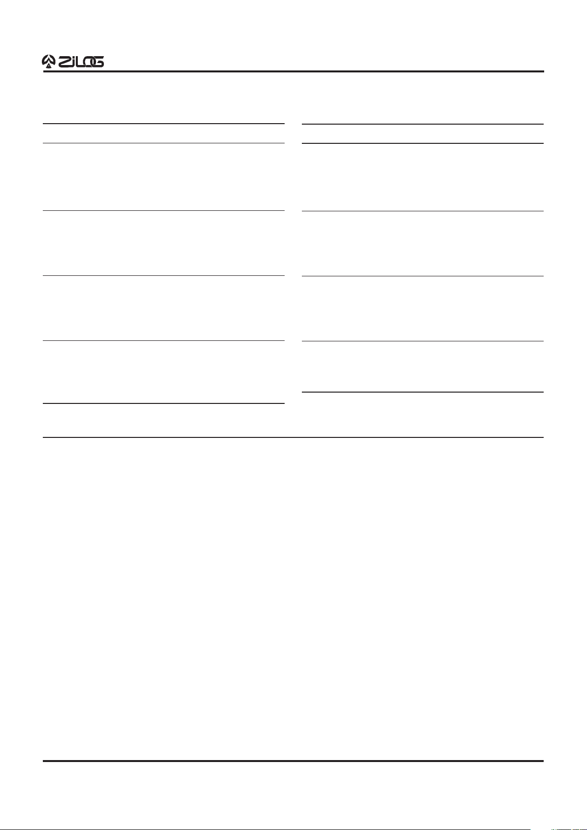
Port 0 (P07-P00). Port 0 is an 8-bit, nibble programmable,
bidirectional, TTL compatible port. These eight I/O lines
can be configured under software control as a nibble I/O
port, or as an address port for interfacing external memory.
When used as an I/O port, Port 0 may be placed under
handshake control. In this configuration, Port 3, lines P32
OEN
Out
In
PAD
Port 0 (I/O)
Handshake Controls
/DAV0 and RDY0
(P32 and P35)
MCU
4
TTL Level Shifter
Auto Latch
R ≈ 500 KΩ
4
Figure 10. Port 0 Configuration
14
Z86C61/62/96
Z8
®
MICROCONTROLLER
PIN FUNCTIONS (Continued)
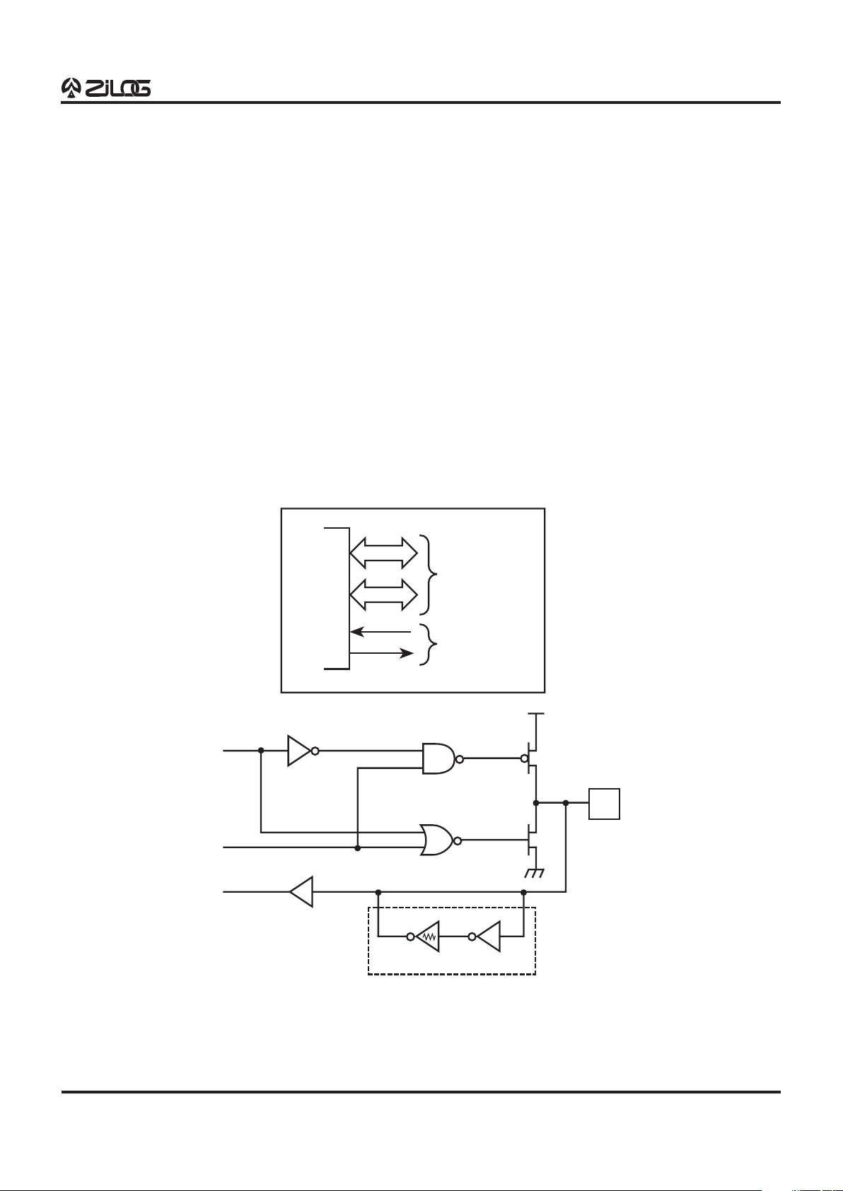
Port 1 (P17-P10). Port 1 is an 8-bit, byte programmable,
bidirectional, TTL compatible port. It has multiplexed Ad-
dress (A7-A0) and Data (D7-D0) ports. For Z86C61/62/96,
these eight I/O lines can be programmed as Input or
Output lines or can be configured under software control
as an address/data port for interfacing external memory.
When used as an I/O port, Port 1 may be placed under
handshake control. In this configuration, Port 3 line P33
and P34 are used as the handshake controls RDY1 and
/DAV1.
Memory locations greater than 16,384 are referenced
through Port 1. To interface external memory, Port 1 must
be programmed for the multiplexed Address/Data mode.
If more than 256 external locations are required, Port 0
must output the additional lines.
Port 1 can be placed in high-impedance state along with
Port 0, /AS, /DS, and R//W, allowing the microcontroller to
share common resources in multiprocessor and DMA
applications. Data transfers can be controlled by assign-
ing P33 as a Bus Acknowledge input, and P34 as a Bus
request output (Figure 11).
OEN
Out
In
PAD
Port 1
(AD7-AD0)
MCU
TTL Level Shifter
Auto Latch
R ≈ 500 KΩ
8
Handshake Controls
/DAV1 and RDY1
(P33 and P34)
Figure 11. Port 1 Configuration
 Loading...