


 Loading...
ZILOG Z8932120FSC, Z8932120PSC, Z8932120VSC, Z8939120VSC, Z8937116FSC Datasheet
...PRELIMINARY PRODUCT SPECIFICATION
1
Z89321/371/391 1
16-BIT DIGITAL SIGNAL PROCESSORS
FEATURES
|
DSP ROM |
OTP |
DSP RAM |
MIPS |
Device |
(KW) |
(KW) |
Lines |
(Max) |
|
|
|
|
|
Z89321 |
4 |
|
512 |
24 |
Z89371 |
|
4 |
512 |
16 |
Z89391 |
64* |
|
512 |
24 |
|
|
|
|
|
Note: *External
■0°C to +70°C Standard Temperature Range -40°C to +85°C Extended Temperature Range
■4.5- to 5.5-Volt Operating Range
DSP Core
■24 MIPS @ 24 MHz Maximum, 16-Bit Fixed Point DSP
■41.7 ns Minimum Instruction Cycle Time
■Six-Level Hardware Stack
■Six Register Address Pointers
■Optimized Instruction Set (30 Instructions)
|
40-Pin |
44-Pin |
44-Pin |
84-Pin |
Device |
DIP |
PLCC |
QFP |
PLCC |
|
|
|
|
|
Z89321 |
X |
X |
X |
|
Z89371 |
X |
X |
X |
|
Z89391 |
|
|
|
X |
|
|
|
|
|
Note: *General-Purpose
On-Board Peripherals
■Dual 8/16-Bit CODEC Interface Capable of up to 10 Mbps
■μ-Law Compression Option (Decompression is Performed in Software)
■16-Bit I/O Bus (Tri-Stated)
■Three I/O Address Pins (Latched Outputs)
■Wait-State Generator
■Three Vectored Interrupts
■13-Bit General-Purpose Timer
GENERAL DESCRIPTION
The Z893XX products are high-performance Digital Signal Processors (DSPs) with a modified Harvard-type architecture featuring separate program and data memory. The design has been optimized for processing power while minimizing silicon space.
The single-cycle instruction execution and bus structure promotes efficient algorithm execution, while the six register pointers provide circular buffering capabilities and dual operand fetching.
Three vectored interrupts are complemented by a six-level stack, and the CODEC interface allows high-speed transfer rates to accommodate digital audio and voice data.
A dedicated Counter/Timer provides the necessary timing signals for the CODEC interface, and an additional 13-bit timer is available for general-purpose use.
DS97DSP0100 |
P R E L I M I N A R Y |
1 |

Z89321/371/391 |
|
16-Bit Digital Signal Processors |
Zilog |
The Z893XX DSPs are optimized to accommodate advanced signal processing algorithms. The 24 MIPS (maximum) operating performance and efficient architecture provides real-time instruction execution. Compression, filtering, frequency detection, audio, voice detection/synthesis, and other vital algorithms can all be accommodated.
The Z89321/371/391 devices feature an on-board CODEC interface, compatible with 8-bit PCM and 16-bit CODECs for digital audio applications. Additionally, an onboard wait-state generator is provided to accommodate slow external peripherals.
For prototypes, as well as production purposes, the Z89371 member of the DSP product family is a one-time
pro-grammable (OTP) device with a 16 MHz maximum operating frequency.
Notes: All signals with a preceding front slash, "/", are active Low. For example, B//W (WORD is active Low); /B/W (BYTE is active Low, only).
Power connections follow conventional descriptions below:
Connection |
Circuit |
Device |
|
|
|
Power |
VCC |
VDD |
Ground |
GND |
VSS |
|
|
|
Program |
Data RAM0 |
|
Data RAM1 |
|
|
|
|
|
|
ROM/OTP |
|
|
|
|||
|
|
|
|
256x16 |
|
256x16 |
|
EA0-2 |
|
|
|
|
4096x16 |
|
|
|
|||
|
|
|
|
|
|
|
|
EXT0-15 |
|
PA0-15 |
PDATA |
|
|
|
|
|
|
|
|
|
|
|
|
|
|
|
/DS |
||
PD0-15 |
PADDR |
|
DDATA |
|
|
|
|
WAIT |
|
|
|
|
|
|
RD//WR |
||||
|
|
|
XDATA |
|
|
|
|
|
|
|
|
|
|
|
|
P0 |
P0 |
|
TXD |
|
|
X |
Y |
|
|
|
|
8/16-Bit, |
|
|
|
|
|
P1 |
P1 |
RXD |
|||
|
|
|
|
|
|
Full Duplex, |
|||
|
|
Multiplier |
|
|
P2 |
P2 |
SCLK |
||
|
|
|
|
10 MBPS |
|||||
|
|
|
|
FS0 |
|||||
|
|
|
|
|
|
DP0-3 |
DP4-6 |
Serial Port |
|
|
|
|
P |
|
|
FS1 |
|||
INT0-2 |
|
|
|
|
|
|
|
||
|
|
|
|
|
|
|
|
|
|
HALT |
|
|
Shifter |
|
|
ADDR |
ADDR |
13-Bit Timer |
|
Program |
|
|
|
GEN0 |
GEN1 |
|
|||
|
|
|
|
|
|
|
|||
/RESET |
Control |
|
|
|
|
|
|
|
UI1-0 |
Unit |
|
|
|
|
|
|
|
||
|
|
|
|
|
|
|
User I/O |
||
|
|
|
|
|
|
|
|
UO1-0 |
|
CLK |
|
Arithmetic |
|
|
|
|
|
||
|
|
|
|
|
|
|
|||
|
|
Logic Unit |
|
|
|
|
|
|
|
|
|
(ALU) |
|
|
|
|
|
|
|
Accumulator |
Figure 1. Z89321/371/391 Functional Block Diagram
2 |
P R E L I M I N A R Y |
DS97DSP0100 |
|
Z89321/371/391 |
Zilog |
16-Bit Digital Signal Processors |
|
|
PIN DESCRIPTION
EXT12 |
|
1 |
|
40 |
|
RXD |
|
|
|||||||
|
|||||||
EXT13 |
|
|
|
|
|
|
VSS |
|
|
|
|
|
|
||
|
|
|
|
|
|
||
EXT14 |
|
|
|
|
|
|
EXT2 |
|
|
|
|
|
|
||
|
|
|
|
|
|
||
VSS |
|
|
|
|
|
|
EXT1 |
|
|
|
|
|
|
||
|
|
|
|
|
|
||
EXT15 |
|
|
|
|
|
|
EXT0 |
|
|
|
|
|
|
||
|
|
|
|
|
|
||
EXT3 |
|
|
|
|
|
|
VSS |
|
|
|
|
|
|
||
|
|
|
|
|
|
||
EXT4 |
|
|
|
|
|
|
FS1 |
|
|
|
|
|
|
||
|
|
|
|
|
|
||
VSS |
|
|
|
|
|
|
U01 |
|
|
|
|
|
|
||
|
|
|
|
|
|
||
EXT5 |
|
|
|
|
|
|
U00 |
|
|
|
|
|
|
||
|
|
|
|
|
|
||
EXT6 |
|
|
|
|
|
/INT0 |
|
|
|
DIP 40 - Pin |
|
||||
EXT7 |
|
|
|
|
|
|
FS0 |
|
|
|
|
|
|
||
|
|
|
|
|
|
||
TXD |
|
|
|
|
|
|
CLK |
|
|
|
|
|
|
||
|
|
|
|
|
|
||
EXT8 |
|
|
|
|
|
|
/DS |
|
|
|
|
|
|
||
|
|
|
|
|
|
||
EXT9 |
|
|
|
|
|
|
VDD |
|
|
|
|
|
|
||
|
|
|
|
|
|
||
VSS |
|
|
|
|
|
|
EA2 |
|
|
|
|
|
|
||
|
|
|
|
|
|
||
EXT10 |
|
|
|
|
|
|
EA1 |
|
|
|
|
|
|
||
|
|
|
|
|
|
||
EXT11 |
|
|
|
|
|
|
EA0 |
|
|
|
|
|
|
||
|
|
|
|
|
|
||
UI1 |
|
|
|
|
|
|
/RESET |
|
|
|
|
|
|
||
|
|
|
|
|
|
||
UI0 |
|
20 |
|
21 |
|
RD//WR |
|
|
|
|
|||||
|
|
|
|||||
SCLK |
|
|
|
VDD |
|||
|
|||||||
|
|||||||
|
|
|
|
|
|||
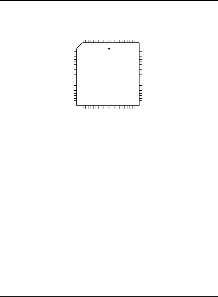
Figure 2. Z89321/371 40-Pin DIP Pin Assignments |
|||||||
Table 1. Z89321/371 40-Pin DIP Pin Identification |
Table 1. Z89321/371 40-Pin DIP Pin Identification |
||||||
No. |
Symbol |
Function |
Direction |
|
|
|
|
1-3 |
EXT12- |
External Data |
Input/Output |
|
EXT14 |
Bus |
|
|
|
|
|
4 |
VSS |
Ground |
|
5 |
EXT15 |
External Data |
Input/Output |
|
|
Bus |
|
|
|
|
|
6-7 |
EXT3-EXT4 |
External Data |
Input/Output |
|
|
Bus |
|
|
|
|
|
8 |
VSS |
Ground |
|
9-11 |
EXT5-EXT7 |
External Data |
Input/Output |
|
|
Bus |
|
|
|
|
|
12 |
TXD |
Serial Output to |
Output |
|
|
CODECs |
|
|
|
|
|
13-14 |
EXT8-EXT9 |
External Data |
Input/Output |
|
|
Bus |
|
|
|
|
|
15 |
VSS |
Ground |
|
16-17 |
EXT10- |
External Data |
Input/Output |
|
EXT11 |
Bus |
|
|
|
|
|
18 |
UI1 |
User Input |
Input |
|
|
|
|
19 |
UI0 |
User Input |
Input |
|
|
|
|
20 |
SCLK |
CODEC Serial |
Input/Output* |
|
|
Clock |
|
|
|
|
|
21 |
VDD |
Power Supply |
Input |
22 |
RD//WR |
Strobes for |
Output |
|
|
External Bus |
|
|
|
|
|
No. |
Symbol |
Function |
Direction |
|
|
|
|
23 |
/RESET |
Reset |
Input |
|
|
|
|
24-26 |
EA0-EA2 |
External Address Output |
|
|
|
Bus |
|
|
|
|
|
27 |
VDD |
Power Supply |
Input |
28 |
/DS |
Data Strobe for |
Output |
|
|
External Bus |
|
|
|
|
|
29 |
CLK |
Clock |
Input |
|
|
|
|
30 |
FS0 |
CODEC 0 Frame Input/Output* |
|
|
|
Sync |
|
|
|
|
|
31 |
/INT0 |
Interrrupt |
Input |
|
|
|
|
32-33 |
UO0-UO1 |
User Output |
Output |
|
|
|
|
34 |
FS1 |
CODEC 1 Frame Input/Output* |
|
|
|
Sync |
|
|
|
|
|
35 |
VSS |
Ground |
|
36-38 |
EXT0-EXT2 |
External Data |
Input/Output |
|
|
Bus |
|
|
|
|
|
39 |
VSS |
Ground |
|
40 |
RXD |
Serial Input from |
Input |
|
|
CODECs |
|
|
|
|
|
Notes:
*Input/Output is defined by interface mode selection. †HALT/WAIT pins not available on 40-pin DIP package.
DS97DSP0100 |
P R E L I M I N A R Y |
3 |
Z89321/371/391 |
|
16-Bit Digital Signal Processors |
Zilog |
PIN DESCRIPTION (Continued)
|
FS1 |
UO1 |
UO0 |
/INT0 |
FSO |
HALT |
CLK |
/DS |
VDD |
EA2 |
EA1 |
|
||
|
6 |
|
|
|
|
|
1 |
|
|
|
|
|
40 |
|
VSS |
7 |
|
|
|
|
|
|
|
|
|
|
|
39 |
EA0 |
EXT0 |
|
|
|
|
|
|
|
|
|
|
|
|
|
/RESET |
EXT1 |
|
|
|
|
|
|
|
|
|
|
|
|
|
WAIT |
EXT2 |
|
|
|
|
|
|
|
|
|
|
|
|
|
RD//WR |
VSS |
|
|
|
|
|
|
|
|
|
|
|
|
|
VDD |
RXD |
|
|
|
|
PLCC 44 -Pin |
|
|
|
SCLK |
|||||
EXT12 |
|
|
|
|
|
|
|
|
|
|
|
|
|
UI0 |
EXT13 |
|
|
|
|
|
|
|
|
|
|
|
|
|
UI1 |
EXT14 |
|
|
|
|
|
|
|
|
|
|
|
|
|
INT1 |
VSS |
|
|
|
|
|
|
|
|
|
|
|
|
|
INT2 |
EXT15 |
17 |
|
|
|
|
|
|
|
|
|
|
|
29 |
EXT11 |
|
18 |
|
|
|
|
|
|
|
|
|
|
|
28 |
|
|
EXT3 |
EXT4 |
VSS |
EXT5 |
EXT6 |
EXT7 |
TXD |
EXT8 |
EXT9 |
VSS |
EXT10 |
|
||
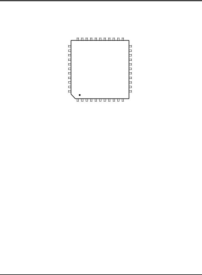
Figure 3. Z89321/371 44-Pin PLCC Pin Assignments
4 |
P R E L I M I N A R Y |
DS97DSP0100 |

|
|
|
Z89321/371/391 |
Zilog |
|
|
16-Bit Digital Signal Processors |
|
|
||
|
Table 2. Z89321/371 44-Pin PLCC Pin Identification |
||
|
|
|
|
No. |
Symbol |
Function |
Direction |
|
|
|
|
1 |
HALT |
Stop Execution |
Input |
|
|
|
|
2 |
FS0 |
CODEC 0 Frame Sync |
Input/Output* |
|
|
|
|
3 |
/INT0 |
Interrupt |
Input |
|
|
|
|
4-5 |
O0-UO1 |
User Output |
Output |
|
|
|
|
6 |
FS1 |
CODEC 1 frame sync |
Input/Output* |
|
|
|
|
7 |
VSS |
Ground |
|
8-10 |
EXT0-EXT2 |
External data bus |
Input/Output |
|
|
|
|
11 |
VSS |
Ground |
|
12 |
RXD |
Serial input from CODECs |
Input |
|
|
|
|
13-15 |
EXT12-EXT14 |
External data bus |
Input/Output |
|
|
|
|
16 |
VSS |
Ground |
|
17 |
EXT15 |
External data bus |
Input/Output |
|
|
|
|
18-19 |
EXT3-EXT4 |
External data bus |
Input/Output |
|
|
|
|
20 |
VSS |
Ground |
|
21-23 |
EXT5-EXT7 |
External data bus |
Input/Output |
|
|
|
|
24 |
TXD |
Serial output to CODECs |
Output |
|
|
|
|
25-26 |
EXT8-EXT9 |
External data bus |
Input/Output |
|
|
|
|
27 |
VSS |
Ground |
|
28-29 |
EXT10-EXT11 |
External data bus |
Input/Output |
|
|
|
|
30 |
/INT2 |
Interrupt |
Input |
|
|
|
|
31 |
/INT1 |
Interrupt |
Input |
|
|
|
|
32 |
UI1 |
User input |
Input |
|
|
|
|
33 |
UI0 |
User input |
Input |
|
|
|
|
34 |
SCLK |
CODEC serial clock |
Input/Output* |
|
|
|
|
35 |
VDD |
Power supply |
Input |
36 |
RD//WR |
RD//WR strobe for EXT bus |
Output |
|
|
|
|
37 |
WAIT |
WAIT state |
Input |
|
|
|
|
38 |
/RESET |
Reset |
Input |
|
|
|
|
39-41 |
EA0-EA2 |
External Address bus |
Output |
|
|
|
|
42 |
VDD |
Power Supply |
Input |
43 |
/DS |
Data strobe for external bus |
Output |
|
|
|
|
44 |
CLK |
Clock |
Input |
|
|
|
|
Note: * Input or output is defined by interface mode selection.
DS97DSP0100 |
P R E L I M I N A R Y |
5 |
Z89321/371/391 |
|
16-Bit Digital Signal Processors |
Zilog |
PIN DESCRIPTION (Continued)
|
FS1 |
UO1 |
UO0 |
/INT0 |
FSO HALT CLK |
/DS |
VDD |
EA2 |
EA1 |
|
|
33 |
|
|
|
|
|
|
23 |
|
|
VSS |
34 |
|
|
|
|
|
|
|
22 |
EA0 |
EXT0 |
|
|
|
|
|
|
|
|
|
/RESET |
EXT1 |
|
|
|
|
|
|
|
|
|
WAIT |
EXT2 |
|
|
|
|
|
|
|
|
|
RD//WR |
VSS |
|
|
|
Z89321/371 |
|
|
|
VDD |
||
RXD |
|
|
|
|
|
|
SCLK |
|||
|
|
|
|
QFP |
|
|
|
|
||
EXT12 |
|
|
|
|
|
|
|
|
UI0 |
|
|
|
|
|
|
|
|
|
|
||
EXT13 |
|
|
|
|
|
|
|
|
|
UI1 |
EXT14 |
|
|
|
|
|
|
|
|
|
INT1 |
VSS |
|
|
|
|
|
|
|
|
|
INT2 |
EXT15 |
44 |
|
|
|
|
|
|
|
12 |
EXT11 |
|
1 |
|
|
|
|
|
|
|
11 |
|
|
EXT3 |
EXT4 |
VSS |
EXT5 |
EXT6 EXT7 TXD |
EXT8 |
EXT9 |
VSS |
EXT10 |
|
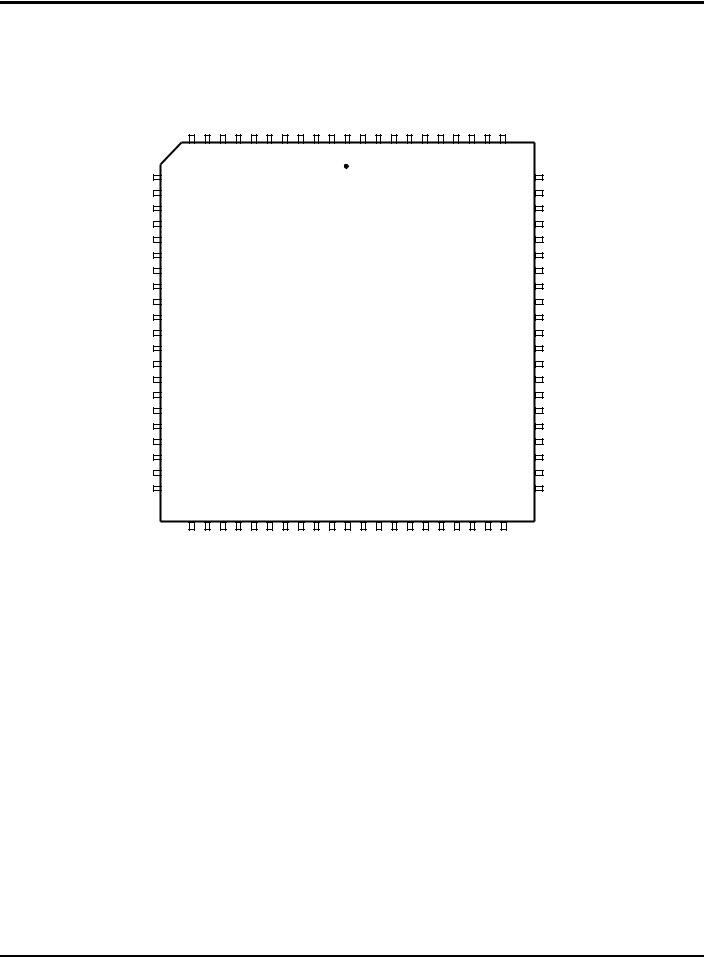
Figure 4. Z89321/371 44-Pin QFP Pin Assignments
6 |
P R E L I M I N A R Y |
DS97DSP0100 |

|
|
|
Z89321/371/391 |
|
Zilog |
|
|
16-Bit Digital Signal Processors |
|
|
|
|
||
|
Table 3. Z89321/371 44-Pin QFP Pin Identification |
|||
|
|
|
|
|
No. |
Symbol |
Function |
Direction |
|
|
|
|
|
|
1-2 |
EXT3-EXT4 |
External data bus |
Input/Output |
|
|
|
|
|
|
3 |
VSS |
Ground |
|
|
4-6 |
EXT5-EXT7 |
External data bus |
Input/Output |
|
|
|
|
|
|
7 |
TXD |
Serial output to CODECs |
Output |
|
|
|
|
|
|
8-9 |
EXT8-EXT9 |
External data bus |
Input/Output |
|
|
|
|
|
|
10 |
VSS |
Ground |
|
|
11-12 |
EXT10-EXT1 |
External data bus |
Input/Output |
|
|
|
|
|
|
13 |
/INT2 |
Interrupt |
Input |
|
|
|
|
|
|
14 |
/INT1 |
Interrupt |
Input |
|
|
|
|
|
|
15 |
UI1 |
User input |
Input |
|
|
|
|
|
|
16 |
UI0 |
User input |
Input |
|
|
|
|
|
|
17 |
SCLK |
CODEC serial clock |
Input/Output* |
|
|
|
|
|
|
18 |
VDD |
Power supply |
Input |
|
19 |
RD//WR |
RD//WR strobe EXT bus |
Output |
|
|
|
|
|
|
20 |
WAIT |
WAIT state |
Input |
|
|
|
|
|
|
21 |
/RESET |
Reset |
Input |
|
|
|
|
|
|
22-24 |
EA0-EA2 |
External address bus |
Output |
|
|
|
|
|
|
25 |
VDD |
Power supply |
Input |
|
26 |
/DS |
Data strobe for external bus |
Output |
|
|
|
|
|
|
27 |
CLK |
Clock |
Input |
|
|
|
|
|
|
28 |
HALT |
Stop execution |
Input |
|
|
|
|
|
|
29 |
FS0 |
CODEC 0 frame sync |
Input/Output* |
|
|
|
|
|
|
30 |
/INT0 |
Interrupt |
Input |
|
|
|
|
|
|
31-32 |
UO0-UO1 |
User output |
Output |
|
|
|
|
|
|
33 |
FS1 |
CODEC 1 frame sync |
Input/Output* |
|
|
|
|
|
|
34 |
VSS |
Ground |
|
|
35-37 |
EXT0-EXT2 |
External data bus |
Input/Output |
|
|
|
|
|
|
38 |
VSS |
Ground |
|
|
39 |
RXD |
Serial input to CODECs |
Input |
|
|
|
|
|
|
40-42 |
EXT12-EXT14 |
External data bus |
Input/Output |
|
|
|
|
|
|
43 |
VSS |
Ground |
|
|
44 |
EXT15 |
External data bus |
Input/Output |
|
|
|
|
|
|
Note: *Input or output is defined by interface mode selection.
DS97DSP0100 |
P R E L I M I N A R Y |
7 |
Z89321/371/391 |
|
16-Bit Digital Signal Processors |
Zilog |
PIN DESCRIPTION (Continued)
|
/PA EN |
EXT15 PA7 VSS |
PA6 |
EXT14 |
PA5 |
EXT13 |
PA4 |
EXT12 |
RXD |
VSS |
PA3 |
EXT2 |
PA2 |
EXT1 |
PA1 |
EXT0 |
VSS |
PA0 |
VDD |
|
11 |
|
|
|
|
|
|
|
1 |
|
|
|
|
|
|
|
|
|
75 |
/EXTEN |
12 |
|
|
|
|
|
|
|
|
|
|
|
|
|
|
|
|
|
74 |
EXT3 |
|
|
|
|
|
|
|
|
|
|
|
|
|
|
|
|
|
|
|
PA8 |
|
|
|
|
|
|
|
|
|
|
|
|
|
|
|
|
|
|
|
EXT4 |
|
|
|
|
|
|
|
|
|
|
|
|
|
|
|
|
|
|
|
PA9 |
|
|
|
|
|
|
|
|
|
|
|
|
|
|
|
|
|
|
|
VSS |
|
|
|
|
|
|
|
|
|
|
|
|
|
|
|
|
|
|
|
EXT5 |
|
|
|
|
|
|
|
|
|
|
|
|
|
|
|
|
|
|
|
PA10 |
|
|
|
|
|
|
|
Z89391 |
|
|
|
|
|
|
|
|
|||
EXT6 |
|
|
|
|
|
|
|
|
|
|
|
|
|
|
|
||||
PA11 |
|
|
|
|
|
|
84-Pin PLCC |
|
|
|
|
|
|
|
|||||
EXT7 |
|
|
|
|
|
|
|
|
|
|
|
|
|
|
|
|
|
|
|
TXD |
|
|
|
|
|
|
|
|
|
|
|
|
|
|
|
|
|
|
|
PA12 |
|
|
|
|
|
|
|
|
|
|
|
|
|
|
|
|
|
|
|
EXT8 |
|
|
|
|
|
|
|
|
|
|
|
|
|
|
|
|
|
|
|
PA13 |
|
|
|
|
|
|
|
|
|
|
|
|
|
|
|
|
|
|
|
EXT9 |
|
|
|
|
|
|
|
|
|
|
|
|
|
|
|
|
|
|
|
VSS |
|
|
|
|
|
|
|
|
|
|
|
|
|
|
|
|
|
|
|
PA14 |
|
|
|
|
|
|
|
|
|
|
|
|
|
|
|
|
|
|
|
EXT10 |
|
|
|
|
|
|
|
|
|
|
|
|
|
|
|
|
|
|
|
PA15 |
|
|
|
|
|
|
|
|
|
|
|
|
|
|
|
|
|
|
|
VDD |
32 |
|
|
|
|
|
|
|
|
|
|
|
|
|
|
|
|
|
54 |
|
33 |
|
|
|
|
|
|
|
|
|
|
|
|
|
|
|
|
|
53 |
|
VSS |
PD0 EXT11 PD1 |
INT2 |
PD2 |
INT1 |
PD3 |
UI1 |
UI0 |
SCLK |
VDD |
RD//WR |
PD4 |
WAIT |
PD5 |
/RESET |
PD6 |
EA0 |
PD7 |
VDD |
Figure 5. Z89391 84-Pin PLCC Pin Assignments
VSS
PD15
FS1
PD14
UO1
PD13
UO0
PD12
INTO
FS0
HALT
PD11
CLK /DS PD10 VDD PD9 EA2 PD8 EA1 /ROMEN
8 |
P R E L I M I N A R Y |
DS97DSP0100 |

|
Z89321/371/391 |
Zilog |
16-Bit Digital Signal Processors |
|
|
Table 4. Z89391 84-Pin PLCC Pin Identification
No. |
Symbol |
Function |
Direction |
|
|
|
|
1 |
RXD |
Serial Input from CODEC |
Input |
|
|
|
|
2 |
EXT12 |
External Data 12 |
In/Output |
|
|
|
|
3 |
PA4 |
Program Address 4 |
Output |
|
|
|
|
4 |
EXT13 |
External Data 13 |
In/Output |
|
|
|
|
5 |
PA5 |
Program Address 5 |
Output |
|
|
|
|
6 |
EXT14 |
External Data 14 |
In/Output |
|
|
|
|
7 |
PA6 |
Program Address 6 |
Output |
|
|
|
|
8 |
VSS |
Ground |
|
9 |
PA7 |
Program Address 7 |
Output |
|
|
|
|
10 |
EXT15 |
External Data 15 |
In/Output |
|
|
|
|
11 |
/PA_EN |
Prog. Mem. Address Enable Input |
|
|
|
|
|
12 |
/EXTEN |
Ext. Bus Enable |
Input |
|
|
|
|
13 |
EXT3 |
External Data 3 |
In/Output |
|
|
|
|
14 |
PA8 |
Program Address 8 |
Output |
|
|
|
|
15 |
EXT4 |
External Data 4 |
In/Output |
|
|
|
|
16 |
PA9 |
Program Address 9 |
Output |
|
|
|
|
17 |
VSS |
Ground |
|
18 |
EXT5 |
External Data 5 |
In/Output |
|
|
|
|
19 |
PA10 |
Program Address 10 |
Output |
|
|
|
|
20 |
EXT6 |
External Data 6 |
In/Output |
|
|
|
|
21 |
PA11 |
Program Address 11 |
Output |
|
|
|
|
22 |
EXT7 |
External Data 7 |
In/Output |
|
|
|
|
23 |
TXD |
Serial Output to CODEC |
Output |
|
|
|
|
24 |
PA12 |
Program Address 12 |
Output |
|
|
|
|
25 |
EXT8 |
External Data 8 |
In/Output |
|
|
|
|
26 |
PA13 |
Program Address 13 |
Output |
|
|
|
|
27 |
EXT9 |
External Data 9 |
In/Output |
|
|
|
|
28 |
VSS |
Ground |
|
29 |
PA14 |
Program Address 14 |
Output |
|
|
|
|
30 |
EXT10 |
External Data 10 |
In/Output |
|
|
|
|
31 |
PA15 |
Program Address 15 |
Output |
|
|
|
|
32 |
VDD |
Power Supply |
Input |
33 |
VSS |
Ground |
|
34 |
PD0 |
Program Data 0 |
Input |
|
|
|
|
35 |
EXT11 |
External Data 11 |
In/Output |
|
|
|
|
36 |
PD1 |
Program Data 1 |
Input |
|
|
|
|
37 |
INT2 |
User Interrupt 2 |
Input |
|
|
|
|
38 |
PD2 |
Program Data 2 |
Input |
|
|
|
|
39 |
INT1 |
User Interrupt 1 |
Input |
|
|
|
|
40 |
PD3 |
Program Data 3 |
Input |
|
|
|
|
41 |
UI1 |
User Input 1 |
Input |
|
|
|
|
42 |
UI0 |
User Input 0 |
Input |
|
|
|
|
Table 4. Z89391 84-Pin PLCC Pin Identification
No. |
Symbol |
Function |
Direction |
|
|
|
|
43 |
SCLK |
CODEC Interface Clock |
In/Output |
|
|
|
|
44 |
VDD |
Power Supply |
Input |
45 |
RD//WR |
R/W External Bus |
Output |
|
|
|
|
46 |
PD4 |
Program Data 4 |
Input |
|
|
|
|
47 |
WAIT |
Wait State Input |
Input |
|
|
|
|
48 |
PD5 |
Program Data 5 |
Input |
|
|
|
|
49 |
/RESET |
Reset |
Input |
|
|
|
|
50 |
PD6 |
Program Data 6 |
Input |
|
|
|
|
51 |
EA0 |
External Address 0 |
Output |
|
|
|
|
52 |
PD7 |
Program Data 7 |
Input |
|
|
|
|
53 |
VDD |
Power Supply |
Input |
54 |
/ROMEN |
ROM Enable |
Input |
|
|
|
|
55 |
EA1 |
External Address 1 |
Output |
|
|
|
|
56 |
PD8 |
Program Data 8 |
Input |
|
|
|
|
57 |
EA2 |
External Address 2 |
Output |
|
|
|
|
58 |
PD9 |
Program Data 9 |
Input |
|
|
|
|
59 |
VDD |
Power Supply |
Input |
60 |
PD10 |
Program Data 10 |
Input |
|
|
|
|
61 |
/DS |
External Data Strobe |
Output |
|
|
|
|
62 |
CLK |
Clock |
Input |
|
|
|
|
63 |
PD11 |
Program Data 11 |
Input |
|
|
|
|
64 |
HALT |
Stop Execution |
Input |
|
|
|
|
65 |
FS0 |
Frame Synch for CODEC |
In/Output |
|
|
Interface 0 |
|
|
|
|
|
66 |
INT0 |
User Interrupt 0 |
Input |
|
|
|
|
67 |
PD12 |
Program Data 12 |
Input |
|
|
|
|
68 |
UO0 |
User Output 0 |
Input |
|
|
|
|
69 |
PD13 |
Program Data 13 |
Input |
|
|
|
|
70 |
UO1 |
User Output 1 |
Input |
|
|
|
|
71 |
PD14 |
Program Data 14 |
Input |
|
|
|
|
72 |
FS1 |
Frame Synch for CODEC |
In/Output |
|
|
Interface 1 |
|
|
|
|
|
73 |
PD15 |
Program Data 15 |
Input |
|
|
|
|
74 |
VSS |
Ground |
|
75 |
VDD |
Power Supply |
Input |
76 |
PA0 |
Program Address 0 |
Output |
|
|
|
|
77 |
VSS |
Ground |
|
78 |
EXT0 |
External Data 0 |
In/Output |
|
|
|
|
79 |
PA1 |
Program Address 1 |
Output |
|
|
|
|
80 |
EXT1 |
External Data 1 |
In/Output |
|
|
|
|
81 |
PA2 |
Program Address 2 |
Output |
|
|
|
|
82 |
EXT2 |
External Data 2 |
In/Output |
|
|
|
|
83 |
PA3 |
Program Address 3 |
Output |
|
|
|
|
84 |
VSS |
Ground |
|
Note: *Input or output is defined by interface mode selection.
DS97DSP0100 |
P R E L I M I N A R Y |
9 |
Z89321/371/391 |
|
16-Bit Digital Signal Processors |
Zilog |
ABSOLUTE MAXIMUM RATINGS
Symbol Description |
Min. |
Max. |
Units |
|
|
|
|
|
|
VCC |
Supply voltage (*) |
–0.3 |
+7.0 |
V |
TSTG |
Storage Temp. |
–65° |
+150 |
°C |
TA |
Oper. Ambient Temp. |
|
† |
°C |
Note:
* Voltage on all pins with respect to GND.
† See Ordering Information.
Stresses greater than those listed under Absolute Maximum Ratings may cause permanent damage to the device. This is a stress rating only; operation of the device at any condition above those indicated in the operational sections of these specifications is not implied. Exposure to absolute maximum rating conditions for extended periods may affect device reliability.
STANDARD TEST CONDITIONS
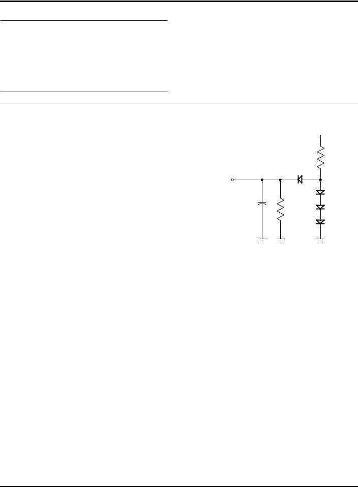
The characteristics listed below apply for standard test conditions as noted. All voltages are referenced to Ground. Positive current flows into the referenced pin (Figure 6).
+5V
2.1 K Ω
From Output
Under Test
30 pF |
9.1 K Ω |
Figure 6. Test Load Diagram
10 |
P R E L I M I N A R Y |
DS97DSP0100 |
|
Z89321/371/391 |
Zilog |
16-Bit Digital Signal Processors |
|
|
DC ELECTRICAL CHARACTERISTICS
(VDD= 5V ±10%, TA = 0°C to +70°C, unless otherwise noted.)
|
|
|
fclock=20 MHz1 |
fclock=16 MHz2 |
fclock=24 MHz3 |
|
|
Sym |
Parameter |
Condition |
Min |
Typ Max. |
Min Typ Max |
Min Typ Max |
Units |
|
|
|
|
|
|
|
|
IDD |
Supply Current |
VDD = 5.5V |
|
70 |
55 |
85 |
mA |
IDC |
DC Power Consumption |
5 |
|
5 |
5 |
5 |
mA |
VIH |
Input High Level |
|
2.7 |
|
2.7 |
2.7 |
V |
VIL |
Input Low Level |
|
|
.8 |
.8 |
.8 |
V |
IL |
Input Leakage |
|
|
10 |
10 |
10 |
μA |
VOH |
Output High Voltage |
IOH =100 μA |
VDD-0.2 |
V |
VDD-0.2 |
VDD-0.2 |
V |
VOL |
Input Low Voltage |
IOL =2.0 mA |
|
.5 |
.5 |
.5 |
V |
IFL |
Output Floating |
|
|
10 |
10 |
10 |
μA |
|
Leakage Current |
|
|
|
|
|
|
|
|
|
|
|
|
|
|
Notes:
1.Z89321 and Z89391 only
2.Z89371 only. VDD = 5V, ± 5% for 16 MHz operation. VDD = 5V, ± 10% for 10 MHz operation.
3.Z89321 only. Limited availability. Contact Zilog sales office.
DC ELECTRICAL CHARACTERISTICS
(VDD = 5V 10%, TA = –40°C to +85°C, unless otherwise specified)
|
|
|
|
fclock = 20 MHz1 |
|
Sym |
Parameter |
Condition |
Min |
Typ |
Max |
|
|
|
|
|
|
IDD |
Supply Current |
VDD=5.5V |
|
70 |
|
IDC |
DC Power Consumption |
|
|
5 |
|
VIH |
Input High Level |
|
2.7 |
|
|
VIL |
Input Low Level |
|
|
|
.8 |
IL |
Input Leakage |
|
|
|
10 |
|
|
|
|
|
|
VOH |
Output High Voltage |
IOH=100 μA |
VDD -0.2 |
|
|
VOL |
Input Low Voltage |
IOL =2.0 mA |
|
|
.5 |
IFL |
Output Floating |
|
|
|
10 |
|
Leakage Current |
|
|
|
|
|
|
|
|
|
|
Notes:
1. Z89321 only
DS97DSP0100 |
P R E L I M I N A R Y |
11 |

Z89321/371/391 |
|
16-Bit Digital Signal Processors |
Zilog |
AC ELECTRICAL CHARACTERISTICS
(VDD= 5V ±10%, TA = 0°C to +70°C, unless otherwise specified.)
|
|
|
fclock = 20 |
|
|
fclock = 24 |
|
||
|
|
|
MHz1 |
fclock = 16 MHz2 |
MHz3 |
|
|||
|
Symbol |
Parameter |
Min |
Max |
Min |
Max |
Min |
Max |
Units |
|
|
|
|
|
|
|
|
|
|
|
Clock |
|
|
|
|
|
|
|
ns |
|
|
|
|
|
|
|
|
|
|
|
TCY |
Clock Cycle Time |
50 |
|
6.25 |
|
41.7 |
|
ns |
|
|
|
|
|
|
|
|
|
|
|
Tr |
Clock Rise Time |
|
2 |
|
2 |
|
2 |
ns |
|
|
|
|
|
|
|
|
|
|
|
Tf |
Clock Fall Time |
|
2 |
|
2 |
|
2 |
ns |
|
|
|
|
|
|
|
|
|
|
|
CPW |
Clock Pulse Width |
23 |
|
29 |
|
19 |
|
ns |
|
|
|
|
|
|
|
|
|
|
|
I/O |
|
|
|
|
|
|
|
|
|
|
|
|
|
|
|
|
|
|
|
DSVALID |
/DS Valid Time from CLOCK Fall |
0 |
15 |
0 |
15 |
0 |
15 |
ns |
|
|
|
|
|
|
|
|
|
|
|
DSHOLD |
/DS Hold Time from CLOCK Rise |
4 |
15 |
4 |
15 |
4 |
15 |
ns |
|
|
|
|
|
|
|
|
|
|
|
EASET |
EA Setup Time to /DS Fall |
12 |
|
12 |
|
12 |
|
ns |
|
|
|
|
|
|
|
|
|
|
|
EAHOLD |
EA Hold Time from /DS Rise |
4 |
|
4 |
|
4 |
|
ns |
|
|
|
|
|
|
|
|
|
|
|
RDSET |
Data Read Setup Time to /DS Rise |
14 |
|
14 |
|
14 |
|
ns |
|
|
|
|
|
|
|
|
|
|
|
RDHOLD |
Data Read Hold Time from /DS Rise |
6 |
|
6 |
|
6 |
|
ns |
|
|
|
|
|
|
|
|
|
|
|
WRVALID |
Data Write Valid Time from /DS Fall |
|
18 |
|
18 |
|
18 |
ns |
|
|
|
|
|
|
|
|
|
|
|
WRHOLD |
Data Write Hold Time from /DS Rise |
5 |
|
5 |
|
5 |
|
ns |
|
|
|
|
|
|
|
|
|
|
|
Interrupt |
|
|
|
|
|
|
|
|
|
|
|
|
|
|
|
|
|
|
|
INTSET |
Interrupt Setup Time to CLOCK Fall |
7 |
|
7 |
|
7 |
|
ns |
|
|
|
|
|
|
|
|
|
|
|
INTWIDTH |
Interrupt Low Pulse Width |
1 TCY |
|
1 TCY |
|
1 TCY |
|
ns |
|
|
|
|
|
|
|
|
|
|
|
CODEC Interface |
|
|
|
|
|
|
|
|
|
|
|
|
|
|
|
|
|
|
|
SSET |
SCLK Setup Time from Clock Rise |
|
15 |
|
15 |
|
15 |
ns |
|
|
|
|
|
|
|
|
|
|
|
FSSET |
FSYNC Setup Time from SCLK Rise |
|
6 |
|
6 |
|
6 |
ns |
|
|
|
|
|
|
|
|
|
|
|
TXSET |
TXD Setup Time from SCLK Rise |
|
7 |
|
7 |
|
7 |
ns |
|
|
|
|
|
|
|
|
|
|
|
RXSET |
RXD Setup Time to SCLK Fall |
7 |
|
7 |
|
7 |
|
ns |
|
|
|
|
|
|
|
|
|
|
|
RXHOLD |
RXD Hold Time from SCLK Fall |
0 |
|
0 |
|
0 |
|
ns |
|
|
|
|
|
|
|
|
|
|
|
Reset |
|
|
|
|
|
|
|
|
|
|
|
|
|
|
|
|
|
|
|
RRISE |
Reset Rise Time |
|
1000 |
|
10000 |
|
1000 |
ns |
|
|
|
|
|
|
|
|
|
|
|
RSET |
Reset Setup Time to CLOCK Rise |
15 |
|
15 |
|
15 |
|
ns |
|
|
|
|
|
|
|
|
|
|
|
RWIDTH |
Reset Low Pulse Width |
2 TCY |
|
2 TCY |
|
2 TCY |
|
ns |
|
|
|
|
|
|
|
|
||
|
External Program Memory |
|
|
|
|
|
|
|
|
|
|
|
|
|
|
|
|
|
|
|
PAVALID |
PA Valid Time from CLOCK Rise |
|
20 |
|
20 |
|
20 |
ns |
|
|
|
|
|
|
|
|
|
|
|
PDSET |
PD Setup Time to CLOCK Rise |
10 |
|
10 |
|
10 |
|
ns |
|
|
|
|
|
|
|
|
|
|
|
PDHOLD |
PD Hold Time from CLOCK Rise |
10 |
|
10 |
|
10 |
|
ns |
|
|
|
|
|
|
|
|
|
|
|
Wait State |
|
|
|
|
|
|
|
|
|
|
|
|
|
|
|
|
|
|
|
WSET |
WAIT Setup Time to CLOCK Rise |
23 |
|
23 |
|
23 |
|
ns |
|
|
|
|
|
|
|
|
|
|
|
WHOLD |
WAIT Hold Time from CLOCK Rise |
1 |
|
1 |
|
1 |
|
ns |
|
|
|
|
|
|
|
|
|
|
|
Halt |
|
|
|
|
|
|
|
|
|
|
|
|
|
|
|
|
|
|
|
HSET |
Halt Setup Time to CLOCK Rise |
3 |
|
3 |
|
3 |
|
ns |
|
|
|
|
|
|
|
|
|
|
|
HHOLD |
Halt Hold Time from CLOCK Rise |
10 |
|
10 |
|
10 |
|
ns |
|
|
|
|
|
|
|
|
|
|
Notes:
1.Z89321 and Z89391 only
2.Z89371 only (VDD = 5V ± 5%)
3.Z89321 only. Limited availability. Contact Zilog sales office.
12 |
P R E L I M I N A R Y |
DS97DSP0100 |
Loading...