


|
Zilog |
P R E L I M I N A R Y |
Z80182/Z8L182 |
|
|
ZILOG INTELLIGENT PERIPHERAL |
|
||
|
|
|
|
|
PRELIMINARY PRODUCT SPECIFICATION
|
|
Z80182/Z8L182 |
|
|
ZILOG INTELLIGENT PERIPHERAL |
|
|
CONTROLLER (ZIP™) |
FEATURES |
|
|
■ Z8S180 MPU |
■ Two ESCC™ Channels with 32-Bit CRC |
|
- Code Compatible with Zilog Z80®/Z180™ CPU |
|
|
- |
Extended Instructions |
■ Three 8-Bit Parallel I/O Ports |
- Operating Frequency: 33 MHz/5V or 20 MHz/3.3V |
|
|
- |
Two DMA Channels |
■ 16550 Compatible MIMIC Interface for |
- |
On-Chip Wait State Generators |
Direct Connection to PC, XT, AT Bus |
- |
Two UART Channels |
|
- |
Two 16-Bit Timer Counters |
■ 100-Pin Package Styles (QFP, VQFP) |
- |
On-Chip Interrupt Controller |
(0.8 Micron CMOS 5120 Technology) |
- On-Chip Clock Oscillator/Generator |
|
|
- |
Clocked Serial I/O Port |
■ Individual WSG for RAMCS and ROMCS |
- |
Fully Static |
|
- |
Low EMI Option |
|
GENERAL DESCRIPTION
The Z80182/Z8L182 is a smart peripheral controller IC for modem (in particular V. Fast applications), fax, voice messaging and other communications applications. It uses the Z80180 microprocessor (Z8S180 MPU core) linked with two channels of the industry standard Z85230 ESCC (Enhanced Serial Communications Controller), 24 bits of parallel I/O, and a 16550 MIMIC for direct connection to the IBM PC, XT, AT bus.
The Z80182/Z8L182 allows complete flexibility for both internal PC and external applications. Also current PC modem software compatibility can be maintained with the Z80182/Z8L182 ability to mimic the 16550 UART chip. The Z80180 acts as an interface between the ESCC™ and 16550 MIMIC interface when used in internal applications, and between the two ESCC channels in the external applications. This interface allows data compression and
error correction on outgoing and incoming data. In external applications, three 8-bit parallel ports are available for driving LEDs or other devices. Figure 1 shows the Z80182/ Z8L182 block diagram, while the pin assignments for the QFP and the VQFP packages are shown in Figures 2 and 3, respectively. All references in this document to the Z80182, or Z182 refer to both the Z80182 and Z8L182.
Notes:
All Signals with a preceding front slash, "/", are active Low, e.g., B//W (WORD is active Low); /B/W (BYTE is active Low, only).
Power connections follow conventional descriptions below:
Connection |
Circuit |
Device |
|
|
|
Power |
VCC |
VDD |
Ground |
GND |
VSS |
DS971820600 |
3-1 |

Zilog |
|
|
|
|
|
|
|
|
|
Z80182/Z8L182 |
P |
R |
E |
L I M |
I |
N |
A |
R |
Y |
ZILOG INTELLIGENT PERIPHERAL |
|
GENERAL DESCRIPTION (Continued) |
|
|
|
|
|
|
|
|
||
D7-D0 |
|
|
|
|
|
|
|
|
|
|
Control |
|
|
|
|
|
|
|
|
GLU |
EV1 |
|
|
|
|
|
|
|
|
|
|
|
A19-A0 |
|
|
|
|
|
|
|
|
Logic |
EV2 |
|
|
|
|
|
|
|
|
|
||
|
Bus |
|
|
|
|
|
|
|
|
|
|
Transceiver |
|
|
|
|
|
|
|
|
|
|
|
|
|
Z8S180 |
|
|
|
|
|
|
Tx Data |
|
|
(Static Z80180) |
|
|
|
|
|
||
|
85230 |
|
|
MPU Core |
|
|
|
|
|
85230 |
|
|
|
|
|
|
|
|
|
||
Rx Data |
ESCC |
|
|
|
|
|
|
|
|
ESCC |
|
Channel |
|
|
|
|
|
|
|
|
Channel |
ESCC |
A |
|
|
|
|
|
|
|
/TRxCB |
B |
|
|
|
|
|
|
|
|
|
||
Control |
|
|
|
|
|
|
|
|
|
|
|
|
|
|
|
|
|
|
|
|
|
/ROMCS |
Address |
|
|
|
|
|
|
|
|
16550 |
|
|
|
|
|
|
|
|
MIMIC |
||
/RAMCS |
Decode |
|
|
|
|
|
|
|
|
|
|
|
|
|
|
|
|
|
Interface |
||
|
|
|
|
|
|
|
|
|
||
|
|
|
|
|
|
|
|
|
|
|
|
8-Bit Parallel |
|
|
8-Bit Parallel |
|
|
|
8-Bit Parallel |
|
|
|
Port C |
|
|
Port B |
|
|
|
|
Port A |
|
85230 ESCC Ch. A or Port C
Z180 Signals 
or Port B
MUX |
|
MUX |
|
MUX |
|
|
|
|
|
16550 MIMIC or ESCC 85230 Ch. B and Port A
Note: Conventional use of the term "MPU side" refers to all interface through the Z180 MPU core and "PC side" refers to all interface through the16550 MIMIC interface.
Figure 1. Z80182/Z8L182 Functional Block Diagram
3-2 |
DS971820600 |

Zilog
/INT0
/INT1/PC6
/INT2/PC7 ST A0 A1 A2 A3 A4 A5 A6 A7 A8 A9
A10
A11
A12
VSS
A13
A14
A15
A16
A17
A18/TOUT
VDD
A19
D0
D1
D2
D3
P R E L I M I N A R Y
|
|
|
/NMI |
/RESET |
|
/BUSREQ |
/BUSACK |
/WAIT |
EXTAL |
|
XTAL |
VSS |
|
PHI |
|
/RD |
/WR |
/M1 |
E |
|
/MRD//MREQ |
/IORQ |
/RFSH |
/HALT |
/SYNCB//HCS |
/RTXCB/HA2 |
RXDB/HA1 |
|
|
|
|||||||||||||||||||||||||||
|
|
|
|
|
|
|
|
|
|
|
|
|
|
|
|
|
|
|
|
|
|
|
|
|
|
|
|
|
|
|
|
|
|
|
|
|
|
|
|
|
|
|
|
|
|
|
|
|
|
|
|
|
|
|
|||
|
|
|
|
|
|
|
|
|
|
|
|
|
|
|
|
|
|
|
|
|
|
|
|
|
|
|
|
|
|
|
|
|
|
|
|
|
|
|
|
|
|
|
|
|
|
|
|
|
|
|
|
|
|
|
|
|
|
|
|
|
|
|
|
|
|
|
|
|
|
|
|
|
|
|
|
|
|
|
|
|
|
|
|
|
|
|
|
|
|
|
|
|
|
|
|
|
|
|
|
|
|
|
|
|
|
|
|
|
|
|
|
|
|
|
|
|
|
|
|
|
100 |
|
|
|
|
|
|
|
|
|
|
|
|
|
|
|
|
|
|
|
|
|
|
|
|
|
|
|
|
|
|
|
|
|
|
|
|
|
|
|
|
|
|
|
|
80 |
|
|
|
||||
|
|
1 |
5 |
|
|
|
|
|
|
|
|
|
|
95 |
|
|
|
|
|
|
|
|
|
|
90 |
|
|
|
|
|
|
|
|
|
85 |
|
|
|
|
|
75 |
|
|
|
|||||||||||||
|
|
|
|
|
|
|
|
|
|
|
|
|
|
|
|
|
|
|
|
|
|
|
|
|
|
|
|
|
|
|
|
|
|
|
|
|
|
|
|
|
|
|
|
|
|
|
|
|
|
|
|
|
|
||||
|
|
|
|
|
|
|
|
|
|
|
|
|
|
|
|
|
|
|
|
|
|
|
|
|
|
|
|
|
|
|
|
|
|
|
|
|
|
|
|
|
|
|
|
|
|
|
|
|
|
|
|
|
|
||||
|
|
|
|
|
|
|
|
|
|
|
|
|
|
|
|
|
|
|
|
|
|
|
|
|
|
|
|
|
|
|
|
|
|
|
|
|
|
|
|
|
|
|
|
|
|
|
|
|
|
|
|
|
|
||||
|
|
|
|
|
|
|
|
|
|
|
|
|
|
|
|
|
|
|
|
|
|
|
|
|
|
|
|
|
|
|
|
|
|
|
|
|
|
|
|
|
|
|
|
|
|
|
|
|
|
|
|
|
|
||||
|
|
|
|
|
|
|
|
|
|
|
|
|
|
|
|
|
|
|
|
|
|
|
|
|
|
|
|
|
|
|
|
|
|
|
|
|
|
|
|
|
|
|
|
|
|
|
|
|
|
|
|
|
|
||||
|
|
|
|
|
|
|
|
|
|
|
|
|
|
|
|
|
|
|
|
|
|
|
|
|
|
|
|
|
|
|
|
|
|
|
|
|
|
|
|
|
|
|
|
|
|
|
|
|
|
|
|
|
|
||||
|
|
|
|
|
10 |
|
|
|
|
|
|
|
|
|
|
|
|
|
|
|
|
|
|
|
|
|
|
|
|
|
|
|
|
|
|
|
|
|
|
|
|
|
|
|
|
|
|
|
|
|
|
|
|
||||
|
|
|
|
|
|
|
|
|
|
|
|
|
|
|
|
|
|
|
|
|
|
|
|
|
|
|
|
|
|
|
|
|
|
|
|
|
|
|
|
|
|
|
|
|
|
|
|
|
|
70 |
|
|
|
||||
|
|
|
|
|
|
|
|
|
|
|
|
|
|
|
|
|
|
|
|
|
|
|
|
|
|
|
|
|
|
|
|
|
|
|
|
|
|
|
|
|
|
|
|
|
|
|
|
|
|
|
|
|
|||||
|
|
|
|
|
|
|
|
|
|
|
|
|
|
|
|
|
|
|
|
|
|
|
|
|
|
|
|
|
|
|
|
|
|
|
|
|
|
|
|
|
|
|
|
|
|
|
|
|
|
|
|
|
|||||
|
|
|
|
|
|
|
|
|
|
|
|
|
|
|
|
|
|
|
|
|
|
|
|
|
|
|
|
|
|
|
|
|
|
|
|
|
|
|
|
|
|
|
|
|
|
|
|
|
|
|
|
|
|||||
|
|
|
|
|
|
|
|
|
|
|
|
|
|
|
|
|
|
|
|
|
|
|
|
|
|
|
|
|
|
|
|
|
|
|
|
|
|
|
|
|
|
|
|
|
|
|
|
|
|
|
|
|
|||||
|
|
|
|
|
|
|
|
|
|
|
|
|
|
|
|
|
|
|
|
|
|
|
|
|
|
|
|
|
|
|
|
|
|
|
|
|
|
|
|
|
|
|
|
|
|
|
|
|
|
|
|
|
|||||
|
|
|
|
|
|
|
|
|
|
|
|
|
|
|
|
|
|
|
|
|
|
|
|
|
|
|
|
|
|
|
|
|
|
|
|
|
|
|
|
|
|
|
|
|
|
|
|
|
|
|
|
|
|||||
|
|
|
|
|
|
|
|
|
|
|
|
|
|
|
|
|
|
|
|
|
|
|
|
|
|
|
|
|
|
|
|
|
|
|
|
|
|
|
|
|
|
|
|
|
|
|
|
|
|
|
|
|
|||||
|
|
|
|
|
15 |
|
|
|
|
|
|
|
|
|
|
|
|
|
|
|
|
Z80182/Z8L182 |
|
|
|
|
|
|
|
|
|
|
|
|
|
|
|
|
|
|
|||||||||||||||||
|
|
|
|
|
|
|
|
|
|
|
|
|
|
|
|
|
|
|
|
|
|
|
|
|
|
|
|
|
|
|
|
|
|
|
|
|
|
|
|
|
|
||||||||||||||||
|
|
|
|
|
|
|
|
|
|
|
|
|
|
|
|
|
|
|
|
|
|
|
|
|
|
|
|
|
|
|
|
|
|
|
|
|
|
|
|
|
|
||||||||||||||||
|
|
|
|
|
|
|
|
|
|
|
|
|
|
|
|
|
|
|
|
|
|
|
|
|
|
|
|
|
|
|
|
|
|
|
|
|
|
|
|
|
|
||||||||||||||||
|
|
|
|
|
|
|
|
|
|
|
|
|
|
|
|
|
|
|
|
|
|
|
|
|
|
|
|
|
|
|
|
|
|
|
|
|
|
|
|
|
|
||||||||||||||||
|
|
|
|
|
|
|
|
|
|
|
|
|
|
|
|
|
|
|
|
|
|
|
|
|
|
|
|
|
|
|
|
|
|
|
|
|
|
|
|
|
|
||||||||||||||||
|
|
|
|
|
|
|
|
|
|
|
|
|
|
|
|
|
|
|
|
|
|
|
|
|
|
|
|
|
|
|
|
|
|
|
|
|
|
|
|
|
|
||||||||||||||||
|
|
|
|
|
|
|
|
|
|
|
|
|
|
|
|
|
|
|
|
|
|
|
|
|
|
|
|
|
|
|
|
|
|
|
|
|
|
|
|
|
|
||||||||||||||||
|
|
|
|
|
|
|
|
|
|
|
|
|
|
|
|
|
|
|
|
|
|
|
|
|
|
|
|
|
|
|
|
|
|
|
|
|
|
|
|
|
|
||||||||||||||||
|
|
|
|
|
20 |
|
|
|
|
|
|
|
|
|
|
|
|
|
|
|
|
|
100-Pin QFP |
|
|
|
|
|
|
|
|
|
|
|
|
|
|
|
65 |
|
|
|
|||||||||||||||
|
|
|
|
|
|
|
|
|
|
|
|
|
|
|
|
|
|
|
|
|
|
|
|
|
|
|
|
|
|
|
|
|
|
|
|
|
|
|
|
||||||||||||||||||
|
|
|
|
|
|
|
|
|
|
|
|
|
|
|
|
|
|
|
|
|
|
|
|
|
|
|
|
|
|
|
|
|
|
|
|
|
|
|
|
|
|
|
|
|
|
|
|
|
|
60 |
|
|
|
||||
|
|
|
|
|
|
|
|
|
|
|
|
|
|
|
|
|
|
|
|
|
|
|
|
|
|
|
|
|
|
|
|
|
|
|
|
|
|
|
|
|
|
|
|
|
|
|
|
|
|
|
|
|
|||||
|
|
|
|
|
|
|
|
|
|
|
|
|
|
|
|
|
|
|
|
|
|
|
|
|
|
|
|
|
|
|
|
|
|
|
|
|
|
|
|
|
|
|
|
|
|
|
|
|
|
|
|
|
|||||
|
|
|
|
|
|
|
|
|
|
|
|
|
|
|
|
|
|
|
|
|
|
|
|
|
|
|
|
|
|
|
|
|
|
|
|
|
|
|
|
|
|
|
|
|
|
|
|
|
|
|
|
|
|||||
|
|
|
|
|
|
|
|
|
|
|
|
|
|
|
|
|
|
|
|
|
|
|
|
|
|
|
|
|
|
|
|
|
|
|
|
|
|
|
|
|
|
|
|
|
|
|
|
|
|
|
|
|
|||||
|
|
|
|
|
|
|
|
|
|
|
|
|
|
|
|
|
|
|
|
|
|
|
|
|
|
|
|
|
|
|
|
|
|
|
|
|
|
|
|
|
|
|
|
|
|
|
|
|
|
|
|
|
|||||
|
|
|
|
|
|
|
|
|
|
|
|
|
|
|
|
|
|
|
|
|
|
|
|
|
|
|
|
|
|
|
|
|
|
|
|
|
|
|
|
|
|
|
|
|
|
|
|
|
|
|
|
|
|||||
|
|
|
|
|
|
|
|
|
|
|
|
|
|
|
|
|
|
|
|
|
|
|
|
|
|
|
|
|
|
|
|
|
|
|
|
|
|
|
|
|
|
|
|
|
|
|
|
|
|
|
|
|
|||||
|
|
|
|
|
25 |
|
|
|
|
|
|
|
|
|
|
|
|
|
|
|
|
|
|
|
|
|
|
|
|
|
|
|
|
|
|
|
|
|
|
|
|
|
|
|
|
|
|
|
|
|
|
|
|
||||
|
|
|
|
|
|
|
|
|
|
|
|
|
|
|
|
|
|
|
|
|
|
|
|
|
|
|
|
|
|
|
|
|
|
|
|
|
|
|
|
|
|
|
|
|
|
|
|
|
|
55 |
|
|
|
||||
|
|
|
|
|
|
|
|
|
|
|
|
|
|
|
|
|
|
|
|
|
|
|
|
|
|
|
|
|
|
|
|
|
|
|
|
|
|
|
|
|
|
|
|
|
|
|
|
|
|
|
|
|
|||||
|
|
|
|
|
|
|
|
|
|
|
|
|
|
|
|
|
|
|
|
|
|
|
|
|
|
|
|
|
|
|
|
|
|
|
|
|
|
|
|
|
|
|
|
|
|
|
|
|
|
|
|
|
|||||
|
|
|
|
|
|
|
|
|
|
|
|
|
|
|
|
|
|
|
|
|
|
|
|
|
|
|
|
|
|
|
|
|
|
|
|
|
|
|
|
|
|
|
|
|
|
|
|
|
|
|
|
|
|||||
|
|
|
|
|
|
|
|
|
|
|
|
|
|
|
|
|
|
|
|
|
|
|
|
|
|
|
|
|
|
|
|
|
|
|
|
|
|
|
|
|
|
|
|
|
|
|
|
|
|
|
|
|
|||||
|
|
|
|
|
|
|
|
|
|
|
|
|
|
|
|
|
|
|
|
|
|
|
|
|
|
|
|
|
|
|
|
|
|
|
|
|
|
|
|
|
|
|
|
|
|
|
|
|
|
|
|
|
|||||
|
|
|
|
|
|
|
|
|
|
|
|
|
|
|
|
|
|
|
|
|
|
|
|
|
|
|
|
|
|
|
|
|
|
|
|
|
|
|
|
|
|
|
|
|
|
|
|
|
|
|
|
|
|||||
|
|
|
|
|
|
|
|
|
|
|
|
|
|
|
|
|
|
|
|
|
|
|
|
|
|
|
|
|
|
|
|
|
|
|
|
|
|
|
|
|
|
|
|
|
|
|
|
|
|
|
|
|
|
|
|||
|
|
|
|
|
30 |
|
|
|
|
|
35 |
|
|
|
|
|
|
|
|
|
|
40 |
|
|
|
|
|
|
|
|
|
45 |
|
|
|
|
|
|
|
|
|
50 |
|
|
|
||||||||||||
|
|
|
|
|
|
|
|
|
|
|
|
|
|
|
|
|
|
|
|
|
|
|
|
|
|
|
|
|
|
|
|
|
|
|
|
|
|
|
|
|
|||||||||||||||||
|
|
|
|
|
|
|
|
|
|
|
|
|
|
|
|
|
|
|
|
|
|
|
|
|
|
|
|
|
|
|
|
|
|
|
|
|
|
|
|
|
|||||||||||||||||
|
|
|
|
|
|
|
|
|
|
|
|
|
|
|
|
|
|
|
|
|
|
|
|
|
|
|
|
|
|
|
|
|
|
|
|
|
|
|
|
|
|||||||||||||||||
|
|
|
|
|
|
|
|
|
|
|
|
|
|
|
|
|
|
|
|
|
|
|
|
|
|
|
|
|
|
|
|
|
|
|
|
|
|
|
|
|
|||||||||||||||||
|
|
|
|
|
|
|
|
|
|
|
|
|
|
|
|
|
|
|
|
|
|
|
|
|
|
|
|
|
|
|
|
|
|
|
|
|
|
|
|
|
|||||||||||||||||
|
|
|
|
|
|
|
|
|
|
|
|
|
|
|
|
|
|
|
|
|
|
|
|
|
|
|
|
|
|
|
|
|
|
|
|
|
|
|
|
|
|||||||||||||||||
|
|
|
|
|
|
|
|
|
|
|
|
|
|
|
|
|
|
|
|
|
|
|
|
|
|
|
|
|
|
|
|
|
|
|
|
|
|
|
|
|
|
|
|
|
|
|
|
|
|
|
|
|
|
|
|
|
|
|
|
|
|
|
|
|
|
|
|
|
|
|
|
|
|
|
|
|
|
|
|
|
|
|
|
|
|
|
|
|
|
|
|
|
|
|
|
|
|
|
|
|
|
|
|
|
|
|
|
|
|
|
|
|
|
|
|
|
|
|
|
|
|
|
|
|
|
|
|
|
|
|
|
|
|
|
|
|
|
|
|
|
|
|
|
|
|
|
|
|
|
|
|
|
|
|
|
|
|
|
|
|
|
|
|
|
|
|
|
|
|
|
|
|
|
|
|
D4 |
D5 |
D6 |
D7 |
/RTS0/PB0 |
/CTS0/PB1 |
/DCD0/PB2 |
TXA0/PB3 |
RXA0/PB4 |
TXA1/PB5 |
RXA1/PB6 |
RXS//CTS1/PB7 |
CKA0//DREQ0 |
VSS |
CKA1//TEND0 |
TXS//DTR//REQB//HINTR |
CKS//W//REQB//HTXRDY |
/DREQ1 |
VDD |
/TEND1//RTSB//HRXRDY |
|
|
|
|||||||||||||||||||||||||||||||||
Figure 2. Z80182/Z8L182 100-Pin QFP Pin Configuration
Z80182/Z8L182
ZILOG INTELLIGENT PERIPHERAL
/TRXCB/HA0
TXDB//HDDIS
/CTSB//HWR
/DCDB//HRD TXDA /TRXCA RXDA
VDD
IEI /IOCS/IEO VSS /RTXCA /SYNCA/PC4 /DCDA/PC0 /CTSA/PC1
/MWR/PC2//RTSA
/DTR//REQA/PC3
/W//REQA/PC5
PA7/HD7
PA6/HD6
PA5/HD5
PA4/HD4
PA3/HD3
PA2/HD2
PA1/HD1
PA0/HD0
EV2
EV1
/ROMCS
/RAMCS
DS971820600 |
3-3 |
Zilog |
|
Z80182/Z8L182 |
P R E L I M I N A R Y |
ZILOG INTELLIGENT PERIPHERAL |
GENERAL DESCRIPTION (Continued)
|
|
|
/CTSB//HWR |
/DCDB//HRD |
TXDA |
/TRXCA |
RXDA |
VDD |
IEI |
/IOCS/IEO |
VSS |
/RTXCA |
/SYNCA/PC4 |
/DCDA/PC0 |
/CTSA/PC1 /MWR/PC2//RTSA |
/DTR//REQA/PC3 |
/W//REQA/PC5 |
PA7/HD7 |
PA6/HD6 |
PA5/HD5 |
|
PA4/HD4 |
PA3/HD3 |
PA2/HD2 |
PA1/HD1 |
PA0/HD0 |
EV2 |
|||||||||||||||||||||||||||||||||
|
|
|
|
|
|
|
|
|
|
|
|
|
|
|
|
|
|
|
|
|
|
|
|
|
|
|
|
|
|
|
|
|
|
|
|
|
|
|
|
|
|
|
|
|
|
|
|
|
|
|
|
|
|
|
|
|
|
|
|
|
|
|
|
|
|
|
|
|
|
|
|
|
|
|
|
|
|
|
|
|
|
|
|
|
|
|
|
|
|
|
|
|
|
|
|
|
|
|
|
|
|
|
|
|
|
|
|
|
|
|
|
|
|
|
|
|
|
|
|
|
|
|
75 |
|
|
|
|
|
|
|
|
70 |
|
|
|
|
|
|
|
|
|
|
65 |
|
|
|
|
|
|
|
|
60 |
|
|
|
|
|
|
|
|
|
55 |
|
|
|
|
|
|
51 |
|||||||||||||
TXDB//HDDIS |
|
76 |
|
|
|
|
|
|
|
|
|
|
|
|
|
|
|
|
|
|
|
|
|
|
|
|
|
|
|
|
|
|
|
|
|
|
|
|
|
|
|
|
|
|
|
|
|
|
|
|
|
|
|
|
|
50 |
||||
|
|
|
|
|
|
|
|
|
|
|
|
|
|
|
|
|
|
|
|
|
|
|
|
|
|
|
|
|
|
|
|
|
|
|
|
|
|
|
|
|
|
|
|
|
|
|
|
|
|
|
|
|||||||||
/TRXCB/HA0 |
|
|
|
|
|
|
|
|
|
|
|
|
|
|
|
|
|
|
|
|
|
|
|
|
|
|
|
|
|
|
|
|
|
|
|
|
|
|
|
|
|
|
|
|
|
|
|
|
|
|
|
|
|
|
|
|
|
|
|
|
|
|
|
|
|
|
|
|
|
|
|
|
|
|
|
|
|
|
|
|
|
|
|
|
|
|
|
|
|
|
|
|
|
|
|
|
|
|
|
|
|
|
|
|
|
|
|
|
|
|
|
|
|
|
|
|
|
|
|
|
|
RXDB/HA1 |
|
|
|
|
|
|
|
|
|
|
|
|
|
|
|
|
|
|
|
|
|
|
|
|
|
|
|
|
|
|
|
|
|
|
|
|
|
|
|
|
|
|
|
|
|
|
|
|
|
|
|
|
|
|
|
|
|
|
|
|
|
|
|
|
|
|
|
|
|
|
|
|
|
|
|
|
|
|
|
|
|
|
|
|
|
|
|
|
|
|
|
|
|
|
|
|
|
|
|
|
|
|
|
|
|
|
|
|
|
|
|
|
|
|
|
|
|
|
|
|
|
/RTXCB/HA2 |
|
|
|
|
|
|
|
|
|
|
|
|
|
|
|
|
|
|
|
|
|
|
|
|
|
|
|
|
|
|
|
|
|
|
|
|
|
|
|
|
|
|
|
|
|
|
|
|
|
|
|
|
|
|
|
|
|
|
|
|
|
|
|
|
|
|
|
|
|
|
|
|
|
|
|
|
|
|
|
|
|
|
|
|
|
|
|
|
|
|
|
|
|
|
|
|
|
|
|
|
|
|
|
|
|
|
|
|
|
|
|
|
|
|
|
|
|
|
|
|
|
/SYNCB//HCS |
|
80 |
|
|
|
|
|
|
|
|
|
|
|
|
|
|
|
|
|
|
|
|
|
|
|
|
|
|
|
|
|
|
|
|
|
|
|
|
|
|
|
|
|
|
|
|
|
|
|
|
|
|
|
|
|
45 |
||||
|
|
|
|
|
|
|
|
|
|
|
|
|
|
|
|
|
|
|
|
|
|
|
|
|
|
|
|
|
|
|
|
|
|
|
|
|
|
|
|
|
|
|
|
|
|
|
|
|
|
|
|
|||||||||
|
|
|
|
|
|
|
|
|
|
|
|
|
|
|
|
|
|
|
|
|
|
|
|
|
|
|
|
|
|
|
|
|
|
|
|
|
|
|
|
|
|
|
|
|
|
|
|
|
|
|
|
|||||||||
/HALT |
|
|
|
|
|
|
|
|
|
|
|
|
|
|
|
|
|
|
|
|
|
|
|
|
|
|
|
|
|
|
|
|
|
|
|
|
|
|
|
|
|
|
|
|
|
|
|
|
|
|
|
|
|
|
|
|
||||
|
|
|
|
|
|
|
|
|
|
|
|
|
|
|
|
|
|
|
|
|
|
|
|
|
|
|
|
|
|
|
|
|
|
|
|
|
|
|
|
|
|
|
|
|
|
|
|
|
|
|
|
|
|
|
|
|||||
/RFSH |
|
|
|
|
|
|
|
|
|
|
|
|
|
|
|
|
|
|
|
|
|
|
|
|
|
|
|
|
|
|
|
|
|
|
|
|
|
|
|
|
|
|
|
|
|
|
|
|
|
|
|
|
|
|
|
|
|
|
|
|
|
|
|
|
|
|
|
|
|
|
|
|
|
|
|
|
|
|
|
|
|
|
|
|
|
|
|
|
|
|
|
|
|
|
|
|
|
|
|
|
|
|
|
|
|
|
|
|
|
|
|
|
|
|
|
|
|
|
|
|
|
/IORQ |
|
|
|
|
|
|
|
|
|
|
|
|
|
|
|
|
|
|
|
|
|
|
|
|
|
|
|
|
|
|
|
|
|
|
|
|
|
|
|
|
|
|
|
|
|
|
|
|
|
|
|
|
|
|
|
|
|
|
|
|
|
|
|
|
|
|
|
|
|
|
|
|
|
|
|
|
|
|
|
|
|
|
|
|
|
|
|
|
|
|
|
|
|
|
|
|
|
|
|
|
|
|
|
|
|
|
|
|
|
|
|
|
|
|
|
|
|
|
|
|
|
/MRD//MREQ |
|
|
|
|
|
|
|
|
|
|
|
|
|
|
|
|
|
|
|
|
|
|
|
|
|
|
|
|
|
|
|
|
|
|
|
|
|
|
|
|
|
|
|
|
|
|
|
|
|
|
|
|
|
|
|
|
|
|
|
|
|
|
|
|
|
|
|
|
|
|
|
|
|
|
|
|
|
|
|
|
|
|
|
|
|
|
|
|
|
|
|
|
|
|
|
|
|
|
|
|
|
|
|
|
|
|
|
|
|
|
|
|
|
|
|
|
|
|
|
|
|
E |
|
85 |
|
|
|
|
|
|
|
|
|
|
|
|
|
|
|
|
|
|
|
|
|
|
|
|
|
|
|
|
|
|
|
|
|
|
|
|
|
|
|
|
|
|
|
|
|
|
|
|
|
|
|
|
|
40 |
||||
|
|
|
|
|
|
|
|
|
|
|
|
|
|
|
|
|
|
|
|
|
|
|
|
|
|
|
|
|
|
|
|
|
|
|
|
|
|
|
|
|
|
|
|
|
|
|
|
|
|
|
|
|||||||||
/M1 |
|
|
|
|
|
|
|
|
|
|
|
|
|
|
|
|
|
|
|
|
|
|
|
|
|
|
|
|
|
|
|
|
|
|
|
|
|
|
|
|
|
|
|
|
|
|
|
|
|
|
|
|
|
|
|
|
||||
|
|
|
|
|
|
|
|
|
|
|
|
|
|
|
|
|
|
|
|
|
|
|
|
|
|
|
|
|
|
|
|
|
|
|
|
|
|
|
|
|
|
|
|
|
|
|
|
|
|
|
|
|
|
|
|
|||||
/WR |
|
|
|
|
|
|
|
|
|
|
|
|
|
|
|
|
|
|
|
|
|
|
|
Z80182/Z8L182 |
|
|
|
|
|
|
|
|
|
|
|
|
|
|
|
|
|
|
|
|
|
|
||||||||||||||
|
|
|
|
|
|
|
|
|
|
|
|
|
|
|
|
|
|
|
|
|
|
|
|
|
|
|
|
|
|
|
|
|
|
|
|
|
|
|
|
|
|
|
|
|
||||||||||||||||
/RD |
|
|
|
|
|
|
|
|
|
|
|
|
|
|
|
|
|
|
|
|
|
|
|
|
|
|
|
|
|
|
|
|
|
|
|
|
|
|
|
|
|
|
|
|
|
|||||||||||||||
|
|
|
|
|
|
|
|
|
|
|
|
|
|
|
|
|
|
|
|
|
|
|
|
|
|
|
|
|
|
|
|
|
|
|
|
|
|
|
|
|
|
|
|
|
||||||||||||||||
PHI |
|
|
|
|
|
|
|
|
|
|
|
|
|
|
|
|
|
|
|
|
|
|
|
100-Pin VQFP |
|
|
|
|
|
|
|
|
|
|
|
|
|
|
|
|
|
|
|
|
|
|
||||||||||||||
|
|
|
|
|
|
|
|
|
|
|
|
|
|
|
|
|
|
|
|
|
|
|
|
|
|
|
|
|
|
|
|
|
|
|
|
|
|
|
|
|
|
|
|
|
||||||||||||||||
VSS |
|
90 |
|
|
|
|
|
|
|
|
|
|
|
|
|
|
|
|
|
|
|
|
|
|
|
|
|
|
|
|
|
|
|
|
|
|
|
|
|
|
|
|
|
|
|
|
|
|
|
|
|
|
|
|
|
35 |
||||
|
|
|
|
|
|
|
|
|
|
|
|
|
|
|
|
|
|
|
|
|
|
|
|
|
|
|
|
|
|
|
|
|
|
|
|
|
|
|
|
|
|
|
|
|
|
|
|
|
|
|
|
|||||||||
XTAL |
|
|
|
|
|
|
|
|
|
|
|
|
|
|
|
|
|
|
|
|
|
|
|
|
|
|
|
|
|
|
|
|
|
|
|
|
|
|
|
|
|
|
|
|
|
|
|
|
|
|
|
|
|
|
|
|
||||
|
|
|
|
|
|
|
|
|
|
|
|
|
|
|
|
|
|
|
|
|
|
|
|
|
|
|
|
|
|
|
|
|
|
|
|
|
|
|
|
|
|
|
|
|
|
|
|
|
|
|
|
|
|
|
|
|||||
EXTAL |
|
|
|
|
|
|
|
|
|
|
|
|
|
|
|
|
|
|
|
|
|
|
|
|
|
|
|
|
|
|
|
|
|
|
|
|
|
|
|
|
|
|
|
|
|
|
|
|
|
|
|
|
|
|
|
|
|
|
|
|
|
|
|
|
|
|
|
|
|
|
|
|
|
|
|
|
|
|
|
|
|
|
|
|
|
|
|
|
|
|
|
|
|
|
|
|
|
|
|
|
|
|
|
|
|
|
|
|
|
|
|
|
|
|
|
|
|
|
|
|
|
/WAIT |
|
|
|
|
|
|
|
|
|
|
|
|
|
|
|
|
|
|
|
|
|
|
|
|
|
|
|
|
|
|
|
|
|
|
|
|
|
|
|
|
|
|
|
|
|
|
|
|
|
|
|
|
|
|
|
|
|
|
|
|
|
|
|
|
|
|
|
|
|
|
|
|
|
|
|
|
|
|
|
|
|
|
|
|
|
|
|
|
|
|
|
|
|
|
|
|
|
|
|
|
|
|
|
|
|
|
|
|
|
|
|
|
|
|
|
|
|
|
|
|
|
/BUSACK |
|
|
|
|
|
|
|
|
|
|
|
|
|
|
|
|
|
|
|
|
|
|
|
|
|
|
|
|
|
|
|
|
|
|
|
|
|
|
|
|
|
|
|
|
|
|
|
|
|
|
|
|
|
|
|
|
|
|
|
|
|
|
|
|
|
|
|
|
|
|
|
|
|
|
|
|
|
|
|
|
|
|
|
|
|
|
|
|
|
|
|
|
|
|
|
|
|
|
|
|
|
|
|
|
|
|
|
|
|
|
|
|
|
|
|
|
|
|
|
|
|
/BUSREQ |
|
95 |
|
|
|
|
|
|
|
|
|
|
|
|
|
|
|
|
|
|
|
|
|
|
|
|
|
|
|
|
|
|
|
|
|
|
|
|
|
|
|
|
|
|
|
|
|
|
|
|
|
|
|
|
|
|
|
|
|
|
|
|
|
|
|
|
|
|
|
|
|
|
|
|
|
|
|
|
|
|
|
|
|
|
|
|
|
|
|
|
|
|
|
|
|
|
|
|
|
|
|
|
|
|
|
|
|
|
|
|
|
|
|
|
|
|
|||||
/RESET |
|
|
|
|
|
|
|
|
|
|
|
|
|
|
|
|
|
|
|
|
|
|
|
|
|
|
|
|
|
|
|
|
|
|
|
|
|
|
|
|
|
|
|
|
|
|
|
|
|
|
|
|
|
|
|
|
30 |
|||
|
|
|
|
|
|
|
|
|
|
|
|
|
|
|
|
|
|
|
|
|
|
|
|
|
|
|
|
|
|
|
|
|
|
|
|
|
|
|
|
|
|
|
|
|
|
|
|
|
|
|
|
|
|
|
|
|||||
/NMI |
|
|
|
|
|
|
|
|
|
|
|
|
|
|
|
|
|
|
|
|
|
|
|
|
|
|
|
|
|
|
|
|
|
|
|
|
|
|
|
|
|
|
|
|
|
|
|
|
|
|
|
|
|
|
|
|
|
|
|
|
|
|
|
|
|
|
|
|
|
|
|
|
|
|
|
|
|
|
|
|
|
|
|
|
|
|
|
|
|
|
|
|
|
|
|
|
|
|
|
|
|
|
|
|
|
|
|
|
|
|
|
|
|
|
|
|
|
|
|
|
|
/INT0 |
|
|
|
|
|
|
|
|
|
|
|
|
|
|
|
|
|
|
|
|
|
|
|
|
|
|
|
|
|
|
|
|
|
|
|
|
|
|
|
|
|
|
|
|
|
|
|
|
|
|
|
|
|
|
|
|
|
|
|
|
|
|
|
|
|
|
|
|
|
|
|
|
|
|
|
|
|
|
|
|
|
|
|
|
|
|
|
|
|
|
|
|
|
|
|
|
|
|
|
|
|
|
|
|
|
|
|
|
|
|
|
|
|
|
|
|
|
|
|
|
|
/INT1/PC6 |
|
|
|
|
|
|
|
|
|
|
|
|
|
|
|
|
|
|
|
|
|
|
|
|
|
|
|
|
|
|
|
|
|
|
|
|
|
|
|
|
|
|
|
|
|
|
|
|
|
|
|
|
|
|
|
|
|
|
|
|
|
|
|
|
|
|
|
|
|
|
|
|
|
|
|
|
|
|
|
|
|
|
|
|
|
|
|
|
|
|
|
|
|
|
|
|
|
|
|
|
|
|
|
|
|
|
|
|
|
|
|
|
|
|
|
|
|
|
|
|
|
/INT2/PC7 |
|
100 |
|
|
|
|
|
|
|
|
|
|
|
|
|
|
|
|
|
|
|
|
|
|
|
|
|
|
|
|
|
|
|
|
|
|
|
|
|
|
|
|
|
|
|
|
|
|
|
|
|
|
|
|
|
26 |
||||
|
|
|
|
|
|
|
|
|
|
|
|
|
|
|
|
|
|
|
|
|
|
|
|
|
|
|
|
|
|
|
|
|
|
|
|
|
|
|
|
|
|
|
|
|
|
|
|
|
|
|
|
|||||||||
|
|
|
|
|
|
|
|
|
|
|
|
|
|
|
|
|
|
|
|
|
|
|
|
|
|
|
|
|
|
|
|
|
|
|
|
|
|
|
|
|
|
|
|
|
|
|
|
|
||||||||||||
|
1 |
|
|
|
|
|
5 |
|
|
|
|
|
|
|
|
|
|
10 |
|
|
|
|
|
|
|
|
15 |
|
|
|
|
|
|
|
|
20 |
|
|
|
|
|
|
|
|
|
25 |
|
|||||||||||||
|
|
|
|
|
|
|
|
|
|
|
|
|
|
|
|
|
|
|
|
|
|
|
|
|
|
|
|
|
|
|
|
|
|
|
|
|
|
|
|
|
|
|
|
|
|
|
|
|
|
|
|
|
|
|
|
|
|
|
|
|
|
|
|
|
|
|
|
|
|
|
|
|
|
|
|
|
|
|
|
|
|
|
|
|
|
|
|
|
|
|
|
|
|
|
|
|
|
|
|
|
|
|
|
|
|
|
|
|
|
|
|
|
|
|
|
|
|
|
|
|
|
|
|
|
ST |
A0 |
|
A1 |
A2 |
|
A3 |
A4 |
|
A5 |
A6 |
|
A7 |
A8 |
|
A9 |
A10 |
|
A11 A12 |
|
VSS |
A13 |
A14 |
|
A15 |
|
A16 |
|
A17 |
|
A18/TOUT |
VDD |
|
A19 |
|
D0 |
|
D1 |
||||||||||||||||||||
Figure 3. Z80182/Z8L182 100-Pin VQFP Pin Configuration
EV1
/ROMCS
/RAMCS
/TEND1//RTSB//HRXRDY VDD
/DREQ1
CKS//W//REQB//HTXRDY
TXS//DTR//REQB/HINTR
CKA1//TEND0 VSS CKA0//DREQ0 RXS//CTS1/PB7 RXA1/PB6 TXA1/PB5 RXA0/PB4 TXA0/PB3 /DCD0/PB2 /CTS0/PB1 /RTS0/PB0
D7
D6
D5
D4
D3
D2
3-4 |
DS971820600 |

Zilog |
P R E L I M I N A R Y |
Z80182/Z8L182 |
ZILOG INTELLIGENT PERIPHERAL |
||
|
|
|
Z180 CPU SIGNALS
A19-A0. Address Bus (input/output, active High, tri-state).
A19-A0 form a 20-bit address bus. The Address Bus provides the address for memory data bus exchanges up to 1 Mbyte, and I/O data bus exchanges up to 64K. The address bus enters a high impedance state during reset and external bus acknowledge cycles, as well as during SLEEP and HALT states. This bus is an input when the external bus master is accessing the on-chip peripherals. Address line A18 is multiplexed with the output of PRT channel 1 (TOUT, selected as address output on reset).
D7-D0. Data Bus (bi-directional, active High, tri-state). D7D0 constitute an 8-bit bi-directional data bus, used for the transfer of information to and from I/O and memory devices. The data bus enters the high impedance state during reset and external bus acknowledge cycles, as well as during SLEEP and HALT states.
/RD. Read (input/output, active Low, tri-state)./RD indicates that the CPU wants to read data from memory or an I/O device. The addressed I/O or memory device should use this signal to gate data onto the CPU data bus.
/WR. Write(input/output,activeLow,tri-state). /WRindicates that the CPU data bus holds valid data to be stored at the addressed I/O or memory location.
/IORQ. I/O Request (input/output, active Low, tri-state).
/IORQ indicates that the address bus contains a valid I/O address for an I/O read or I/O write operation. /IORQ is also generated, along with /M1, during the acknowledgment of the /INT0 input signal to indicate that an interrupt response vector can be placed onto the data bus. This signal is analogous to the IOE signal of the Z64180.
/M1. Machine Cycle 1 (input/output, active Low). Together with /MREQ, /M1 indicates that the current cycle is the opcode fetch cycle of an instruction execution; unless /M1E bit in the OMCR is cleared to 0. Together with /IORQ, /M1 indicates that the current cycle is for an interrupt acknowledge. It is also used with the /HALT and ST signals to decode status of the CPU machine cycle. This signal is analogous to the /LIR signal of the Z64180.
/MREQ. Memory Request (input/output, active Low, tristate). /MREQ indicates that the address bus holds a valid address for a memory read or memory write operation. This signal is analogous to the /ME signal of the Z64180. /MREQ is multiplexed with /MRD on the /MRD//MREQ pin. The /MRD//MREQ pin is an input during adapter modes; is tri-state during bus acknowledge if the /MREQ function is selected; and is inactive High if /MRD function is selected.
/MRD. Memory Read (input/output, active Low, tri-state).
/MRD is active when both the internal /MREQ and /RD are active. /MRD is multiplexed with /MREQ on the /MRD //MREQ pin. The /MRD//MREQ pin is an input during adapter modes; is tri-state during bus acknowledge if /MREQ function is selected; and is inactive High if /MRD function is selected. The default function on power up is /MRD and may be changed by programming bit 3 of the Interrupt Edge/Pin MUX Register (xxDFH).
/MWR. Memory Write (input/output, active Low, tri-state).
/MWR is active when both the internal /MREQ and /WR are active. This /RTSA or PC2 combination is pin multiplexed with/MWRonthe/MWR/PC2//RTSApin.Thedefaultfunction of this pin on power up is /MWR, which may be changed by programming bit 3 in the Interrupt Edge/Pin MUX Register (xxDFH).
/WAIT. (input/output active Low). /WAIT indicates to the MPU that the addressed memory or I/O devices are not ready for a data transfer. This input is used to induce additional clock cycles into the current machine cycle. The /WAIT input is sampled on the falling edge of T2 (and subsequent wait states). If the input is sampled Low, then additional wait states are inserted until the /WAIT input is sampled High, at which time execution will continue.
/HALT. Halt/Sleep Status (input/output, active Low). This output is asserted after the CPU has executed either the HALT or SLEEP instruction, and is waiting for either nonmaskable or maskable interrupts before operation can resume. It is also used with the /M1 and ST signals to decode status of the CPU machine cycle. On exit of HALT/ SLEEP mode, the first instruction fetch can be delayed by 16 clock cycles after the /HALT pin goes High, if HALT 16 feature is selected.
/BUSACK. Bus Acknowledge (input/output, active Low).
/BUSACK indicates to the requesting device, the MPU address and data bus, and some control signals, have entered their high impedance state.
/BUSREQ. Bus Request (input, active Low). This input is used by external devices (such as DMA controllers) to request access to the system bus. This request has a higher priority than /NMI and is always recognized at the end of the current machine cycle. This signal will stop the CPU from executing further instructions and places the address/data buses and other control signals, into the high impedance state.
DS971820600 |
3-5 |

Zilog |
|
Z80182/Z8L182 |
P R E L I M I N A R Y |
ZILOG INTELLIGENT PERIPHERAL |
Z180 CPU SIGNALS (Continued)
/NMI. Non-maskable interrupt (input, negative edge triggered). /NMI has a higher priority than /INT and is always recognized at the end of an instruction, regardless of the state of the interrupt enable flip-flops. This signal forces CPU execution to continue at location 0066H.
/INT0. Maskable Interrupt Request 0 (input/output active Low). This signal is generated by external I/O devices. The CPU will honor this request at the end of the current instruction cycle as long as the /NMI and /BUSREQ signals are inactive. The CPU acknowledges this interrupt request with an interrupt acknowledge cycle. During this cycle, both the /M1 and /IORQ signals become active. The internal Z180 MPU’s /INT0 source is: /INT0 or ESCC or the MIMIC. This input is level triggered. /INT0 is an open-drain output, so you can connect other open-drain interrupts onto the circuit in addition to haveing a pull-up to VCC.
/INT1, /INT2. Maskable Interrupt Requests 1 and 2 (inputs, active Low). This signal is generated by external I/O devices. The CPU will honor these requests at the end of the current instruction cycle as long as the /NMI, /BUSREQ, and /INT0 signals are inactive. The CPU acknowledges these interrupt requests with an interrupt acknowledge cycle. Unlike the acknowledgment for /INT0, during this cycle neither the /M1 or /IORQ signals become active. These pins may be programmed to provide an active Low level on rising or falling edge interrupts. The level of the external /INT1 and /INT2 pins may be read through bits PC6 and PC7 of parallel Port C. Pin /INT1/PC6 multiplexes /INT1 and PC6. Pin /INT2/PC7 multiplexes /INT2 and PC7.
/RFSH. Refresh (input/output, active Low, tri-state).
Together with /MREQ, /RFSH indicates that the current CPU machine cycle and the contents of the address bus should be used for refresh of dynamic memories. The low order 8 bits of the address bus (A7-A0) contain the refresh address. This signal is analogous to the /REF signal of the Z64180.
Z180 MPU UART AND SIO SIGNALS
CKA0, CKA1. Asynchronous Clocks 0 and 1 (bi-directional, active High). These pins are the transmit and receive clocks for the synchronous channels. CKA0 is multiplexed with /DREQ0 on the CKA0//DREQ0 pin. CKA1 is multiplexed with /TEND0 on the CKA1//TEND0 pin.
CKS. Serial Clock (bi-directional, active High). This line is clock for the CSIO channel and is multiplexed with the ESCC signal (/W//REQB) and the 16550 MIMIC interface signal /HTxRDY on the CKS//W//REQB//HTxRDY pin.
/DCD0. Data Carrier Detect 0 (input, active Low). This is a programmable modem control signal for ASCI channel 0. /DCD0 is multiplexed with the PB2 (parallel Port B, bit 2) on the /DCD0/PB2 pin.
/RTS0. Request to Send 0 (output, active Low). This is a programmable modem control signal for ASCI channel 0. This pin is multiplexed with PB0 (parallel Port B, bit 0) on the /RTS0/PB0 pin.
/CTS0. Clear to Send 0 (input, active Low). This line is a modem control signal for the ASCI channel 0. This pin is multiplexed with PB1 (parallel Port B, bit 1) on the /CTS0 /PB1 pin.
TxA0. Transmit Data 0 (output, active High). This signal is the transmitted data from the ASCI channel 0. This pin is multiplexed with PB3 (parallel Port B, bit 3) on the TxA0/PB3 pin.
TxS. Clocked Serial Transmit Data (output, active High). This line is the transmitted data from the CSIO channel. TxS is multiplexed with the ESCC signal (/DTR//REQB) and the 16550 MIMIC interface signal HINTR on the TxS//DTR //REQB//HINTR pin.
RxA0. Receive Data 0 (input, active High). This signal is the receive data to ASCI channel 0. This pin is multiplexed with PB4 (parallel Port B, bit 4) on the RxA0/PB4.
RxS. Clocked Serial Receive Data (input, active High).
This line is the receive data for the CSIO channel. RxS is multiplexed with the /CTS1 signal for ASCI channel 1 and with PB7 (parallel Port B, bit 7) on the RxS//CTS1/PB7 pin.
RxA1. Received Data ASCI channel 1 (input, active High).
This pin is multiplexed with PB6 (parallel Port B, bit 6) on the RxA1/PB6 pin.
TxA1. Transmitted Data ASCI Channel 1 (output, active High). This pin is multiplexed with PB5 (parallel Port B, bit 5) on the TxA1/PB5 pin.
3-6 |
DS971820600 |

Zilog |
P R E L I M I N A R Y |
Z80182/Z8L182 |
ZILOG INTELLIGENT PERIPHERAL |
||
|
|
|
Z180 MPU DMA SIGNALS
/TEND0. Transfer End 0 (output, active Low). This output is asserted active during the last write cycle of a DMA operation. It is used to indicate the end of the block transfer. /TEND0 is multiplexed with CKA1 on the CKA1//TEND0 pin.
/TEND1. Transfer End 1 (output, active Low). This output is asserted active during the last write cycle of a DMA operation. It is used to indicate the end of the block transfer. /TEND1 is multiplexed with the ESCC signal /RTSB and the 16550 MIMIC interface signal /HRxRDY on the /TEND1//RTSB//HRxRDY pin.
/DREQ0. DMA request 0 (input, active Low). /DREQ0 is used to request a DMA transfer from DMA channel 0. The DMA channel monitors the input to determine when an external device is ready for a read or write operation. This input can be programmed to be either level or edge sensed. /DREQ0 is multiplexed with CKA0 on the CKA0//DREQ0 pin.
/DREQ1. DMA request 1 (input, active Low). /DREQ1 is used to request a DMA transfer from DMA channel 1. The DMA channel monitors the input to determine when an external device is ready for a read or write operation. This input can be programmed to be either level or edge sensed.
Z180™ MPU TIMER SIGNALS
TOUT. Timer Out (output, active High). TOUT is the pulse output from PRT channel 1. This line is multiplexed with A18 of the address bus on the A18/TOUT pin.
Z85230 ESCC™ SIGNALS
TxDA. Transmit Data (output, active High). This output signal transmits channel A’s serial data at standard TTL levels. This output can be tri-stated during power down modes.
TxDB. Transmit Data (output, active High). This output signal transmits channel B’s serial data at standard TTL levels. In Z80182/Z8L182 mode 1, TxDB is multiplexed with the 16550 MIMIC interface /HDDIS signal on the TxDB//HDDIS pin.
RxDA. Receive Data (inputs, active High). These inputs receive channel A’s serial data at standard TTL levels.
RxDB. Receive Data (input, active High). These inputs receive channel B’s serial data at standard TTL levels. In Z80182/Z8L182 mode 1 RxDB is multiplexed with the 16550 MIMIC HA1 input on the RxDB/HA1 pin.
/TRxCA. Transmit/Receive Clock (input or output, active Low). The functions of this pin are under channel A program control. /TRxCA may supply the receive clock or the transmit clock in the Input mode or supply the output of the digital phase-locked loop, the crystal oscillator, the baud rate generator, or the transmit clock in the output mode.
/TRxCB. Transmit/Receive Clock (input or output, active Low). The functions of this pin are under channel B program
control. /TRxCB may supply the receive clock or the transmit clock in the input mode or supply the output of the Digital Phase-Locked Loop (DPLL), the crystal oscillator, the baud rate generator, or the transmit clock in output mode. In Z80182/Z8L182 mode 1 /TRxCB is multiplexed with the 16550 MIMIC interface HA0 input on the /TRxCB/HA0 pin.
/RTxCA. Receive/Transmit Clock (input, active Low). The functions of this pin are under channel A program control. In channel A, /RTxCA may supply the receive clock, the transmit clock, the clock for the baud rate generator, or the clock for the DPLL. This pin can also be programmed for use by the /SYNCA pin as a crystal oscillator. The receive clock may be 1, 16, 32, or 64 times the data rate in asynchronous mode.
/RTxCB. Receive/Transmit Clock (input, active Low). The functions of this pin are under channel B program control. In channel B, /RTxCB may supply the receive clock, the transmit clock, the clock for the baud rate generator, or the clock for the DPLL. This pin can also be programmed for use by the /SYNCB pin as a crystal oscillator. The receive clock may be 1, 16, 32, or 64 times the data rate in asynchronous mode. In Z80182/Z8L182 mode 1 the /RTxCB signal is multiplexed with 16550 MIMIC interface HA2 input on the /RTxCB/HA2 pin.
DS971820600 |
3-7 |

Zilog |
|
Z80182/Z8L182 |
P R E L I M I N A R Y |
ZILOG INTELLIGENT PERIPHERAL |
Z85230 ESCC SIGNALS (Continued)
/SYNCA, /SYNCB. Synchronization (inputs/outputs, active Low). These pins can act as either inputs, outputs, or as part of the crystal oscillator circuit. In the Asynchronous Receive mode (crystal oscillator option not selected), these pins are inputs similar to /CTS and /DCD. In this mode, transitions on these lines affect the state of the Sync /Hunt status bits in Read Register 0, but have no other function. /SYNCA is also multiplexed with PC4 (parallel Port C, bit 4) on the /SYNCA/PC4 pin.
In External Synchronization mode with the crystal oscillator not selected, these lines also act as inputs. In this mode /SYNC must be driven Low two receive clock cycles after the last bit in the sync character is received. Character assembly begins on the rising edge of the receive clock immediately preceding the activation of /SYNC.
In the Internal Synchronization mode, (Monosync and Bisync) with the crystal oscillator not selected, these pins act as outputs and are active only during the part of the receive clock cycle in which sync characters are recognized. The sync condition is not latched, so these outputs are active each time a sync character is recognized (regardless of the character boundaries). In SDLC mode, these pins act as outputs and are valid on receipt of a flag. In Z80182/Z8L182 mode 1 the /SYNCB signal is multiplexed with the 16550 MIMIC interface /HCS input on the /SYNCB //HCS pin.
/CTSA. Clear To Send (input, active Low). If this pin is programmed as auto enable, a Low on this input enables the channel A transmitter. If not programmed as auto enable, it may be used as a general-purpose input. The input is Schmitt-trigger buffered to accommodate slow rise-time input. The ESCC™ detects transitions on this input and can interrupt the Z180™ MPU on either logic level transitions. /CTSA is multiplexed with PC1 (parallel Port C, bit 1) on the /CTSA/PC1 pin.
/CTSB. Clear To Send (input, active Low). This pin is similar to /CTSA’s functionality but is applicable to the channel B transmitter. In Z80182/Z8L182 mode, the /CTSB signal is multiplexed with the 16550 MIMIC interface /HWR input on the /CTSB //HWR pin.
/DCDA. Data Carrier Detect (input, active Low). This pin functions as receiver enables if it is programmed as an auto enable bit; otherwise, it may be used as a generalpurpose input pin. The pin is Schmitt-trigger buffered to accommodate slow rise-time signals. The ESCC detects transitions on this pin and can interrupt the Z180 MPU on either logic level transitions. /DCDA is also multiplexed with PC0 (parallel Port C, bit 0) on the /DCDA/PC0 pin.
/DCDB. Data Carrier Detect (input, active Low). This pin’s functionality is similar to /DCDA but applicable to the channel B receiver. In Z80182/Z8L182 mode 1, /DCDB is multiplexed with the 16550 MIMIC interface /HRD input on the /DCDB//HRD pin.
/RTSA. Request to Send (output, active Low). When the Request to Send (RTS) bit in Write Register 5 channel A is set, the /RTSA signal goes Low. When the RTS bit is reset in the Asynchronous mode and auto enables is on, the signal goes High after the transmitter is empty. In Synchronous mode or in Asynchronous mode with auto enables off, the /RTSA pin strictly follows the state of the RTS bit. The pin can be used as general-purpose output. /RTSA is multiplexed with PC2 (parallel Port C bit 2). This /RTSA or PC2 combination is pin multiplexed with /MWR (active when both the internal /MREQ and /WR are active) on the /MWR/PC2//RTSA pin. The default function of this pin on power-up is /MWR which may be changed by programming bit 3 in the Interrupt Edge/Pin MUX Register (xxDFH).
/RTSB. Request to Send (output, active Low). This pin is similar in functionality as /RTSA but is applicable on channel B. The /RTSB signal is multiplexed with the Z180 MPU /TEND1 signal and the 16550 MIMIC interface /HRxRDY signal on the /TEND1//RTSB//HRxRDY pin.
/DTR//REQA. Data Terminal Ready (output, active Low).
This pin functions as it is programmed into the DTR bit. It can also be used as general-purpose output (transmit) or as request lines for the DMA controller. The ESCC allows full duplex DMA transfers. /DTR//REQA is also multiplexed with PC3 (parallel Port C, bit 3) on the /DTR//REQA /PC3 pin.
/DTR//REQB. Data Terminal Ready (output, active Low).
This pin functions as it is programmed into the DTR bit. It can also be used as general-purpose output (transmit) or as request lines for the DMA controller. The ESCC allows full duplex DMA transfers. The /DTR//REQB signal is multiplexed with the Z180 MPU TxS signal and the 16550 MIMIC interface HINTR signal on the /TxS//DTR//REQB //HINTR pin.
/W//REQA. Wait/Request (output, open drain when programmed for the Wait function, driven High or Low when programmed for a Request function). This dualpurpose output can be programmed as Request (receive) lines for a DMA controller or as Wait lines to synchronize the Z180 MPU to the ESCC data rate. The reset state is Wait. The ESCC allows full duplex DMA transfers. /W//REQA is also multiplexed with PC5 (parallel Port C, bit 5) on the /W//REQA/PC5 pin.
3-8 |
DS971820600 |

Zilog |
P R E L I M I N A R Y |
Z80182/Z8L182 |
ZILOG INTELLIGENT PERIPHERAL |
||
|
|
|
/W//REQB. Wait/Request (output, open drain when programmed for the Wait function, driven High or Low when programmed for a Request function). This pin is similar in functionality to /W//REQA but is applicable on
channel B. The /W//REQB signal is multiplexed with the Z180 MPU CKS signal and the 16550 MIMIC interface /HTxRDY signal on the CKS//W//REQB//HTxRDY pin.
16550 MIMIC INTERFACE SIGNALS
HD7-HD0. HostDataBus(input/output,tri-state). InZ80182/ Z8L182 mode 1, the host data bus is used to communicate between the 16550 MIMIC interface and the PC/XT/AT. It is multiplexed with the PA7-PA0 of parallel Port A when the Z80182/Z8L182 is in mode 0.
/HDDIS. HostDriverDisable(output,activeLow).InZ80182/ Z8L182 mode 1, this signal goes Low whenever the PC/XT/AT is reading data from the 16550 MIMIC interface. In Z80182/Z8L182 mode 0, this pin is multiplexed with the ESCC™ TxDB signal on the TxDB//HDDIS pin.
HA2-HA0. Host Address (input). In Z80182/Z8L182 mode 1, these pins are the address inputs to the 16550 MIMIC interface. This address determines which register the PC/XT/AT accesses. HA0 is multiplexed with /TRxCB on the /TRxCB/HA0 pin; HA1 is multiplexed with RxDB on the RxDB/HA1 pin; HA2 is multiplexed with /RTxCB on the /RTxCB/HA2 pin.
/HCS. Host Chip Select (input, active Low). In Z80182/ Z8L182 mode 1, this input is used by the PC/XT/AT to select the 16550 MIMIC interface for an access. In Z80182/ Z8L182 mode 0, it is multiplexed with the ESCC /SYNCB signal on the SYNCB//HCS pin.
/HWR. Host Write (Input, active Low). In Z80182/Z8L182 mode 1, this input is used by the PC/XT/AT to signal the 16550 MIMIC interface that a write operation is taking place. In Z80182/Z8L182 mode 0, this input is multiplexed with the ESCC /CTSB signal on the /CTSB//HWR pin.
/HRD. Host Read (input, active Low). In Z80182/Z8L182 mode 1, this input is used by the PC/XT/AT to signal the 16550 MIMIC interface that a read operation is taking place. In Z80182/Z8L182 mode 0, this pin is multiplexed with the ESCC /DCDB signal on the /DCDB//HRD pin.
HINTR. Host Interrupt (output, active High). In Z80182/ Z8L182 mode 1, this output is used by the 16550 MIMIC interface to signal the PC/XT/AT that an interrupt is pending. In Z80182/Z8L182 mode 0, this pin is multiplexed with the ESCC (/DTR//REQB) signal and the Z180 MPU TxS signal on the TxS//DTR//REQB//HINTR pin.
/HTxRDY. Host Transmit Ready (output, active Low). In Z80182/Z8L182 mode 1, this output is used by the 16550 MIMIC in DMA mode to signal the PC/XT/AT that the Transmit Holding Register is empty. In Z80182/Z8L182 mode 0, this pin is multiplexed with the ESCC (/W//REQB) signal and the Z180 MPU CKS signal on the CKS//W// REQB//HTxRDY pin.
/HRxRDY. Host Receive Ready (output, active Low). In Z80182/Z8L182 mode 1, this output is used by the 16550 MIMIC interface in DMA mode to signal the PC/XT/AT that a data byte is ready in the Receive Buffer. In Z80182/ Z8L182 mode 0, this pin is multiplexed with the ESCC /RTSB signal and the Z180 MPU /TEND1 signal on the /TEND1/RTSB /HRxRDY pin.
PARALLEL PORTS
PA7-PA0. Parallel Port A (input/output). These lines can be configured as inputs or outputs on a bit-by-bit basis when the Z80182/Z8L182 is operated in mode 0. These pins are multiplexed with the HD7-HD0 when the Z80182/Z8L182 is in mode 1.
PB7-PB0. Parallel Port B (input/output). These lines can be configured as inputs or outputs on a bit-by-bit basis when the Port function is selected in the System Configuration register. The pins are multiplexed with the following Z180 peripheral functions: /RTS0, /CTS0, /DCD0, TxA0, RxA0, TxA1, RxA1, (RxS//CTS1).
PC7-PC0. Parallel Port C (input/output). These lines can be configured as inputs or outputs on a bit-by-bit basis for bits PC5-PC0. Bits PC7 and PC6 are input only and read the level of the external /INT2 and /INT1 pins. When /INT2 and/or /INT1 are in edge capture mode, writing a 1 to the respective PC7, PC6 bit clears the interrupt capture latch; writing a 0 has no effect. Bits PC5-PC0 are multiplexed with the following pins from ESCC channel A: (/W//REQA), /SYNCA, (/DTR//REQA), /RTSA, /MWR, /CTSA, /DCDA. The Port function is selected through a bit in the System Configuration Register.
DS971820600 |
3-9 |

Zilog |
|
Z80182/Z8L182 |
P R E L I M I N A R Y |
ZILOG INTELLIGENT PERIPHERAL |
EMULATION SIGNALS
EV1, EV2. Emulation Select (input). These two pins determine the emulation mode of the Z180 MPU (Table 1).
Table 1. Evaluation Modes
Mode |
EV2 |
EV1 |
Description |
|
|
|
|
0 |
0 |
0 |
Normal mode, on-chip Z180 bus master |
1 |
0 |
1 |
Emulation Adapter Mode |
2 |
1 |
0 |
Emulator Probe Mode |
3 |
1 |
1 |
Reserved for Test |
|
|
|
|
SYSTEM CONTROL SIGNALS
ST. Status (output, active High). This signal is used with the /M1 and /HALT output to decode the status of the CPU machine cycle. If unused, this pin should be pulled to VDD.
/RESET. Reset Signal (input, active Low). /RESET signal is used for initializing the MPU and other devices in the system. It must be kept in the active state for a period of at least three system clock cycles.
IEI. Interrupt Enable Signal (input, active High). IEI is used with the IEO to form a priority daisy chain when there is more than one interrupt-driven peripheral.
IEO. Interrupt Enable Output Signal (output, active High).
Inthedaisy-chaininterruptcontrol,IEOcontrolstheinterrupt of external peripherals. IEO is active when IEI is 1 and the CPU is not servicing an interrupt from the on-chip peripherals. This pin is multiplexed with /IOCS on the /IOCS/IEO pin. The /IOCS function is the default on Power On or Reset conditions and is changed by programming bit 2 in the Interrupt Edge/Pin MUX Register.
/IOCS. Auxiliary Chip Select Output Signal (output, active Low). This pin is multiplexed with /IEO on the /IOCS/IEO pin. /IOCS is an auxiliary chip select that decodes A7, A6, /IORQ, /M1 and effectively decodes the address space xx80H to xxBFH for I/O transactions. A15 through A8 are not decoded so that the chip select is active in all pages of I/O address space. The /IOCS function is the default on the /IOCS/IEO pin after Power On or Reset conditions and is changed by programming bit 2 in the Interrupt Edge/Pin MUX Register.
/RAMCS. RAM Chip Select (output, active Low). Signal used to access RAM based upon the Address and the RAMLBR and RAMUBR registers and /MREQ.
/ROMCS. ROM Chip Select (output, active Low). Signal used to access ROM based upon the address and the ROMBR register and /MREQ.
E. Enable Clock (output, active High). Synchronous machine cycle clock output during bus transactions.
XTAL. Crystal (input, active High). Crystal oscillator connection. This pin should be left open if an external clock is used instead of a crystal. The oscillator input is not a TTL level (reference DC characteristics).
EXTAL. External Clock/Crystal (input, active High). Crystal oscillator connections to an external clock can be input to the Z80180 on this pin when a crystal is not used. This input is Schmitt triggered.
PHI. System Clock (output, active High). The output is used as a reference clock for the MPU and the external system. The frequency of this output is reflective of the functional speed of the processor. In clock divide-by-two mode, the pHI frequency is half that of the crystal or input clock. If divide-by-one mode is enabled, the PHI frequency is equivalent to that of crystal or input frequency. The PHI frequency is also fed to the ESCC core. If running over 20 MHz (5V) or 10 MHz (3V) the PHI-ESCC frequency divider should be enabled to divide the PHI clock by two prior to feeding into the ESCC core.
3-10 |
DS971820600 |
Zilog |
P R E L I M I N A R Y |
Z80182/Z8L182 |
ZILOG INTELLIGENT PERIPHERAL |
||
|
|
|
MULTIPLEXED PIN DESCRIPTIONS
A18/TOUT. During Reset, this pin is initialized as an A18 pin. If either TOC1 or TOC0 bit of the Timer Control Register
(TCR) is set to 1, The TOUT function is selected. If TOC1 and TOC0 bits are cleared to 0, the A18 function is selected.
In normal user mode (on-chip bus master), the A18 signal for the chip select logic is obtained from the CPU before the external pin is muxed as A18/TOUT. Therefore, the selection of TOUT will not affect the operation of the 182 chip select logic. However, in adapter mode (off-chip bus master), the A18 signal MUST be provided by the external bus master.
CKA0//DREQ0. During Reset, this pin is initialized as CKA0 pin. If either DM1 or SM1 in the DMA Mode Register (DMODE) is set to 1, /DREQ0 function is always selected.
CKA1//TEND0. During Reset, this pin is initialized as CKA1 pin. If CKA1D bit in the ASCI control register Ch1(CNTLA1) is set to 1, /TEND0 function is selected. If CKA1D bit is set to 0, CKA1 function is selected.
RxS//CTS1. During Reset, this pin is initialized as the RxS pin. If CTS1E bit in the ASCI status register Ch1 (STAT1) is set to 1, /CTS1 function is selected. If CTS1E bit is set to 0, RxS function is selected. This pin is also multiplexed with PB7 based on bit 6 in the System Configuration Register.
The pins below are triple-multiplexed based upon the values of bit 1 and bit 2 of the System Configuration Register. The pins are configured as Table 2 specifies. On Reset, both bits 1 and 2 are 0, so /TEND1,TxS,CKS are selected.
Table 2. Triple Multiplexed Pins
Bit 1 |
Bit 2 |
Master Configuration Register |
|
|
|
0 |
0 |
/TEND1,TxS,CKS |
0 |
1 |
/RTSB,/DTR//REQB,/W//REQB |
1 |
0 |
/TEND1,TxS,CKS |
1 |
1 |
/HRxRDY,//HTxRDY,HINTR |
|
|
|
The pins below are multiplexed based upon the value of bit 1 of the System Configuration register. If bit 1 is 0, then the Z80182/Z8L182 Mode 0 (non-16550 MIMIC mode) signals are selected; if bit 1 is 1, then Z80182/Z8L182 Mode 1 (16550 MIMIC mode) signals are selected. On Reset, Z80182/Z8L182 Mode 0 is always selected as shown in Table 3.
Table 3. Mode 0 and Mode 1 Multiplexed Pins
Z80182/Z8L182 |
Z80182/Z8L182 |
Mode 0 |
Mode 1 |
|
|
TxDB |
/HDDIS |
RxDB |
HA1 |
/TRxCB |
HA0 |
/RTxCB |
HA2 |
/SYNCB |
/HCS |
/CTSB |
/HWR |
/DCDB |
/HRD |
PA7-PA0 |
HD7-HD0 |
|
|
DS971820600 |
3-11 |

Zilog |
|
Z80182/Z8L182 |
P R E L I M I N A R Y |
ZILOG INTELLIGENT PERIPHERAL |
Ports B and C Multiplexed Pin Descriptions
Ports B and C are pin multiplexed with the Z180 ASCI functions and part of ESCC channel A. The MUX function iscontrolledbybits7-5intheSystemConfigurationRegister. The MUX is organized as shown in Table 4.
Table 4. Multiplexed Port Pins
Port Mode |
ASCI/ESCC Mode |
Function |
Function |
|
|
PB7 |
RxS,/CTS1 |
PB6 Select with bit 6=1 |
RxA1 |
PB5 System Config Reg. |
TxA1 |
PB4 |
RxA0 |
PB3 |
TxA0 |
PB2 Select with bit 5=1 |
/DCD0 |
PB1 System Config Reg. |
/CTS0 (Note 1) |
PB0 |
/RTS0 |
PC7 |
Always Reads /INT2 Ext. |
|
Status |
PC6 |
Always Reads /INT1 Ext. |
|
Status |
PC5 |
/W//REQA |
PC4 |
/SYNCA |
PC3 Select with bit 7=1 |
/DTR//REQA |
PC2 System Config Reg. |
/RTSA (Note 2) |
PC1 |
/CTSA |
PC0 |
/DCDA |
|
|
Note 1:
When the Port function (PB1) is selected, the internal Z180/ CTS0 is always driven Low. This ensures that the ASCI channel 0 of the Z180™ MPU is enabled to transmit data.
Note 2:
Interrupt Edge /Pin MUX register, bit 3 chooses between the /MWR or PC2//RTSA combination; the System Configuration Register bit 7 chooses between PC2 and /RTSA.
Refer to Table 5 for the 1st, 2nd and 3rd pin functions.
3-12 |
DS971820600 |

Zilog |
|
P |
R E L I M |
I N A R Y |
Z80182/Z8L182 |
|
ZILOG INTELLIGENT PERIPHERAL |
||||
|
|
|
|
||
|
|
Table 5. Primary, Secondary and Tertiary Pin Functions |
|
||
|
|
|
|
|
|
Pin Number |
1st |
2nd |
3rd |
MUX |
|
VQFP |
QFP |
Function |
Function |
Function |
Control |
|
|
|
|
|
|
1 |
4 |
ST |
|
|
|
2 |
5 |
A0 |
|
|
|
3 |
6 |
A1 |
|
|
|
4 |
7 |
A2 |
|
|
|
5 |
8 |
A3 |
|
|
|
|
|
|
|
|
|
6 |
9 |
A4 |
|
|
|
7 |
10 |
A5 |
|
|
|
8 |
11 |
A6 |
|
|
|
9 |
12 |
A7 |
|
|
|
10 |
13 |
A8 |
|
|
|
|
|
|
|
|
|
11 |
14 |
A9 |
|
|
|
12 |
15 |
A10 |
|
|
|
13 |
16 |
A11 |
|
|
|
14 |
17 |
A12 |
|
|
|
15 |
18 |
VSS |
|
|
|
16 |
19 |
A13 |
|
|
|
17 |
20 |
A14 |
|
|
|
18 |
21 |
A15 |
|
|
|
19 |
22 |
A16 |
|
|
|
20 |
23 |
A17 |
|
|
|
|
|
|
|
|
|
21 |
24 |
A18/TOUT |
|
|
|
22 |
25 |
VDD |
|
|
|
23 |
26 |
A19 |
|
|
|
24 |
27 |
D0 |
|
|
|
25 |
28 |
D1 |
|
|
|
|
|
|
|
|
|
26 |
29 |
D2 |
|
|
|
27 |
30 |
D3 |
|
|
|
28 |
31 |
D4 |
|
|
|
29 |
32 |
D5 |
|
|
|
30 |
33 |
D6 |
|
|
|
|
|
|
|
|
|
31 |
34 |
D7 |
|
|
|
32 |
35 |
/RTS0 |
PB0 |
|
SYS CONF REG Bit 5 |
33 |
36 |
/CTS0 |
PB1 |
|
SYS CONF REG Bit 5 |
34 |
37 |
/DCD0 |
PB2 |
|
SYS CONF REG Bit 5 |
35 |
38 |
TxA0 |
PB3 |
|
SYS CONF REG Bit 5 |
|
|
|
|
|
|
36 |
39 |
RxA0 |
PB4 |
|
SYS CONF REG Bit 5 |
37 |
40 |
TxA1 |
PB5 |
|
SYS CONF REG Bit 6 |
38 |
41 |
RxA1 |
PB6 |
|
SYS CONF REG Bit 6 |
39 |
42 |
RxS//CTS1 |
PB7 |
|
SYS CONF REG Bit 6 |
40 |
43 |
CKA0//DREQ0 |
|
|
|
|
|
|
|
|
|
DS971820600 |
3-13 |

Zilog |
|
|
|
|
Z80182/Z8L182 |
|
|
P R E L I M I N A R Y |
ZILOG INTELLIGENT PERIPHERAL |
||
MULTIPLEXED PIN DESCRIPTIONS (Continued) |
|
|
|||
|
|
Table 5. Primary, Secondary and Tertiary Pin Functions (Continued) |
|||
|
|
|
|
|
|
Pin Number |
1st |
2nd |
3rd |
MUX |
|
VQFP |
QFP |
Function |
Function |
Function |
Control |
|
|
|
|
|
|
41 |
44 |
VSS |
|
|
|
42 |
45 |
CKA1//TEND0 |
|
|
|
43 |
46 |
TxS |
/DTR//REQB |
HINTR |
SYS CONF REG Bit 1,2 |
44 |
47 |
CKS |
/W//REQB |
/HTxRDY |
SYS CONF REG Bit 1,2 |
45 |
48 |
/DREQ1 |
|
|
|
|
|
|
|
|
|
46 |
49 |
VDD |
/RTSB |
/HRxRDY |
SYS CONF REG Bit 1,2 |
47 |
50 |
/TEND1 |
|||
48 |
51 |
/RAMCS |
|
|
|
49 |
52 |
/ROMCS |
|
|
|
50 |
53 |
EV1 |
|
|
|
|
|
|
|
|
|
51 |
54 |
EV2 |
|
|
|
52 |
55 |
PA0 |
HD0 |
|
SYS CONF REG Bit 1 |
53 |
56 |
PA1 |
HD1 |
|
SYS CONF REG Bit 1 |
54 |
57 |
PA2 |
HD2 |
|
SYS CONF REG Bit 1 |
55 |
58 |
PA3 |
HD3 |
|
SYS CONF REG Bit 1 |
|
|
|
|
|
|
56 |
59 |
PA4 |
HD4 |
|
SYS CONF REG Bit 1 |
57 |
60 |
PA5 |
HD5 |
|
SYS CONF REG Bit 1 |
58 |
61 |
PA6 |
HD6 |
|
SYS CONF REG Bit 1 |
59 |
62 |
PA7 |
HD7 |
|
SYS CONF REG Bit 1 |
60 |
63 |
/W//REQA |
PC5 |
|
SYS CONF REG Bit 7 |
|
|
|
|
|
|
61 |
64 |
/DTR//REQA |
PC3 |
|
SYS CONF REG Bit 7 |
62 |
65 |
/MWR |
PC2 |
RTSA |
SYS CONF REG Bit 7 * |
63 |
66 |
/CTSA |
PC1 |
|
SYS CONF REG Bit 7 |
64 |
67 |
/DCDA |
PC0 |
|
SYS CONF REG Bit 7 |
65 |
68 |
/SYNCA |
PC4 |
|
SYS CONF REG Bit 7 |
|
|
|
|
|
|
66 |
69 |
/RTxCA |
|
|
|
67 |
70 |
VSS |
IEO |
|
INT EDG/PIN REG Bit 2 |
68 |
71 |
/IOCS |
|
||
69 |
72 |
IEI |
|
|
|
70 |
73 |
VDD |
|
|
|
3-14 |
DS971820600 |

Zilog |
|
P |
R E L I |
M I N A R Y |
Z80182/Z8L182 |
|
ZILOG INTELLIGENT PERIPHERAL |
||||
|
|
|
|||
|
|
Table 5. Primary, Secondary and Tertiary Pin Functions (Continued) |
|||
|
|
|
|
|
|
Pin Number |
1st |
2nd |
3rd |
MUX |
|
VQFP |
QFP |
Function |
Function |
Function |
Control |
|
|
|
|
|
|
71 |
74 |
RxDA |
|
|
|
72 |
75 |
/TRxCA |
|
|
|
73 |
76 |
TxDA |
|
|
|
74 |
77 |
/DCDB |
/HRD |
|
SYS CONF REG Bit 1 |
75 |
78 |
/CTSB |
/HWR |
|
SYS CONF REG Bit 1 |
|
|
|
|
|
|
76 |
79 |
TxDB |
/HDDIS |
|
SYS CONF REG Bit 1 |
77 |
80 |
/TRxCB |
HA0 |
|
SYS CONF REG Bit 1 |
78 |
81 |
RxDB |
HA1 |
|
SYS CONF REG Bit 1 |
79 |
82 |
/RTxCB |
HA2 |
|
SYS CONF REG Bit 1 |
80 |
83 |
/SYNCB |
/HCS |
|
SYS CONF REG Bit 1 |
|
|
|
|
|
|
81 |
84 |
/HALT |
|
|
|
82 |
85 |
/RFSH |
|
|
|
83 |
86 |
/IORQ |
|
|
|
84 |
87 |
/MRD |
/MREQ |
|
INT EDG/PIN REG Bit 3 |
85 |
88 |
E |
|
|
|
|
|
|
|
|
|
86 |
89 |
/M1 |
|
|
|
87 |
90 |
/WR |
|
|
|
88 |
91 |
/RD |
|
|
|
89 |
92 |
PHI |
|
|
|
90 |
93 |
VSS |
|
|
|
91 |
94 |
XTAL |
|
|
|
92 |
95 |
EXTAL |
|
|
|
93 |
96 |
/WAIT |
|
|
|
94 |
97 |
/BUSACK |
|
|
|
95 |
98 |
/BUSREQ |
|
|
|
|
|
|
|
|
|
96 |
99 |
/RESET |
|
|
|
97 |
100 |
/NMI |
|
|
|
98 |
1 |
/INT0 |
|
|
|
99 |
2 |
/INT1 |
PC6** |
|
|
100 |
3 |
/INT2 |
PC7** |
|
|
Notes:
*Also controlled by Interrupt Edge/Pin MUX Register
**PC7 and PC6 are inputs only and can read values of /INT1 and /INT2.
DS971820600 |
3-15 |
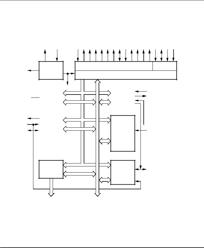
Zilog |
|
Z80182/Z8L182 |
P R E L I M I N A R Y |
ZILOG INTELLIGENT PERIPHERAL |
Z80182/Z8L182 FUNCTIONAL DESCRIPTION
Functionally, the on-chip Z182 MPU and ESCC™ are the same as the discrete devices (Figure 1). Therefore, for a detailed description of each individual unit, refer to the
Product Specification/Technical Manuals of each discrete product. The following subsections describe each of the individual units of the Z182.
Z182 MPU FUNCTIONAL DESCRIPTION
This unit provides all the capabilities and pins of the Zilog Z8S180 MPU (Static Z80180 MPU). Figure 4 shows the S180 MPU Block Diagram of the Z182. This allows 100%
software compatibility with existing Z180™ (and Z80®) software. The following is an overview of the major functional units of the Z182.
XTAL |
EXTAL |
/RESET |
/RD |
/WR |
/M1 |
/MREQ |
/IORQ |
/HALT |
/WAIT |
/BUSREQ |
/BUSACK |
/RFSH |
ST |
E |
/NMI |
/INT0 |
/INT1 |
/INT2 |
|
Timing & |
Bus State Control |
Interrupt |
Ø |
Clock |
|
|
|
Generator |
CPU |
|
A18  /TOUT
/TOUT
16-Bit |
|
|
/DREQ1 |
Programmable |
|
DMACs |
/TEND |
Reload Timers |
|
(2) |
|
(2) |
|
|
|
|
|
|
|
TxS |
Clocked |
|
|
RxS//CTS |
Serial I/O |
CKS |
Port |
|
MMU
Address Bus (16-Bit) |
Data Bus (8-Bit) |
 TxA0
TxA0

 CKA0 /DREQ0
Asynchronous
SCI RxA0 (Channel 0)  /RTS0
/RTS0
 /CTS0
/CTS0  /DCD0
/DCD0
 TxA1
TxA1
Asynchronous
SCI CKA1 /TEND0
(Channel 1)  RxA1
RxA1
A19-A0 |
D7-D0 |
Figure 4. S180 MPU Block Diagram of Z182
3-16 |
DS971820600 |

Zilog |
P R E L I M I N A R Y |
Z80182/Z8L182 |
ZILOG INTELLIGENT PERIPHERAL |
||
|
|
|
Z182 CPU
The Z182 CPU is 100% software compatible with the Z80® CPU and has the following additional features:
Faster Execution Speed. The Z182 CPU is “fine tuned,” making execution speed, on average, 10% to 20% faster than the Z80 CPU.
Enhanced DRAM Refresh Circuit. Z182 CPU’s DRAM refresh circuit does periodic refresh and generates an 8-bit refresh address. It can be disabled or the refresh period adjusted, through software control.
Enhanced Instruction Set. The Z182 CPU has seven additional instructions to those of the Z80 CPU, which include the MLT (Multiply) instruction.
HALT and Low Power Modes of Operation. The Z182 CPU has HALT and Low Power modes of operation, which are ideal for the applications requiring low power consumption like battery operated portable terminals.
System Stop Mode. When the Z182 is in System Stop mode, it is only the Z180 MPU that is in STOP mode.
Standby and Idle Mode. Please refer to the Z8S180 Product Specification for additional information on these two additional Low Power modes.
Instruction Set. The instruction set of the Z182 CPU is identical to the Z180. For more details about each transaction, please refer to the Product Specification/ Technical Manual for the Z180/Z80 CPU.
Z182 CPU Basic Operation
Z182 CPU’s basic operation consists of the following events. These are identical to the Z180 MPU. For more details about each operation, please refer to the Product Specification/Technical Manual for the Z180.
■Operation Code Fetch Cycle
■Memory Read/Write Operation
■Input/Output Operation
■Bus Request/Acknowledge Operation
■Maskable Interrupt Request Operation
■Trap and Non-Maskable Interrupt Request Operation
■HALT and Low Power Modes of Operation
■Reset Operation
Memory Management Unit (MMU)
The Memory Management Unit (MMU) allows the user to map the memory used by the CPU (64 Kbytes of logical addressing space) into 1 Mbyte of physical addressing space. The organization of the MMU allows object code compatibility with the Z80 CPU while offering access to an extended memory space. This is accomplished by using an effective common area-banked area scheme.
DMA Controller
The Z182 MPU has two DMA controllers. Each DMA controller provides high-speed data transfers between memory and I/O devices. Transfer operations supported are memory-to-memory, memory-to/from-I/O, and I/O-to- I/O. Transfer modes supported are request, burst, and cycle steal. The DMA can access the full 1 Mbytes addressing range with a block length up to 64 Kbytes and can cross over 64K boundaries.
Asynchronous Serial Communication Interface (ASCI)
This unit provides two individual full-duplex UARTs. Each channel includes a programmable baud rate generator and modem control signals. The ASCI channels also support a multiprocessor communication format.
Programmable Reload Timer (PRT)
The Z182 MPU has two separate Programmable Reload Timers, each containing a 16-bit counter (timer) and count reload register. The time base for the counters is system clock divided by 20. PRT channel 1 provides an optional output to allow for waveform generation.
Clocked Serial I/O (CSI/O)
The CSI/O channel provides a half-duplex serial transmitter and receiver. This channel can be used for simple highspeed data connection to another CPU or MPU.
Programmable Wait State Generator
To ease interfacing with slow memory and I/O devices, the Z182 MPU unit has a programmable wait state generator. By programming the DMA/WAIT Control Register (DCNTL), up to three wait states are automatically inserted in memory and I/O cycles. This unit also inserts wait states during onchip DMA transactions. When using RAMCS and ROMCS wait state generators, the wait state controller with the most programmed wait states will determine the number of wait states inserted.
DS971820600 |
3-17 |

Zilog |
|
Z80182/Z8L182 |
P R E L I M I N A R Y |
ZILOG INTELLIGENT PERIPHERAL |
Z85230 ESCC™ FUNCTIONAL DESCRIPTION
The Zilog Enhanced Serial Communication Controller ESCC™ isadualchannel,multiprotocoldatacommunication peripheral. The ESCC functions as a serial-to-parallel, parallel-to-serial converter/controller. The ESCC can be software-configured to satisfy a wide variety of serial communicationsapplications.Thedevicecontainsavariety of new, sophisticated internal functions including on-chip baud rate generators, digital phase-lock loops, and crystal oscillators, which dramatically reduce the need for external logic.
The ESCC handles asynchronous formats, synchronous byte-oriented protocols such as IBM® Bisync, and synchronous bit-oriented protocols such as HDLC and IBM SDLC. This versatile device supports virtually any serial data transfer application (telecommunication, LAN, etc.)
The device can generate and check CRC codes in any synchronous mode and can be programmed to check data integrity in various modes. The ESCC also has facilities for modem control in both channels in applications where these controls are not needed, the modem controls can be used for general-purpose I/O.
With access to 14 Write registers and 7 Read registers per channel (number of the registers varies depending on the version), the user can configure the ESCC to handle all synchronous formats regardless of data size, number of stop bits, or parity requirements. The ESCC also accommodates all synchronous formats including character, byte, and bit-oriented protocols.
Within each operating mode, the ESCC also allows for protocol variations by checking odd or even parity bits, character insertion or deletion, CRC generation, checking break and abort generation and detection, and many other protocol-dependent features.
The ESCC (Enhanced SCC) is pin and software compatible to the CMOS SCC version. The following enhancements were made to the CMOS SCC:
■Deeper Transmit FIFO (4 bytes)
■Deeper Receive FIFO (8 bytes)
■Programmable FIFO interrupt and DMA request level
■Seven enhancements to improve SDLC link layer supports:
-Automatic transmission of the opening flag
-Automatic reset of Tx Underrun/EOM latch
-Deactivation of /RTS pin after closing flag
-Automatic CRC generator preset
-Complete CRC reception
-TxD pin automatically forced High with NRZI encoding when using mark idle
-Status FIFO handles better frames with an ABORT
-Receive FIFO automatically unlocked for special receive interrupts when using the SDLC status FIFO
■Delayed bus latching for easier microprocessor interface
■New programmable features added with Write Register 7' (WR seven prime)
■Write registers, 3, 4, 5 and 10 are now readable
■Read register 0 latched during access
■DPLL counter output available as jitter-free transmitter clock source
■Enhanced /DTR, /RTS deactivation timing
3-18 |
DS971820600 |

Zilog |
P R E L I M I N A R Y |
Z80182/Z8L182 |
ZILOG INTELLIGENT PERIPHERAL |
||
|
|
|
The following features are common to both the ESCC and the CMOS SCC:
■Two independent full-duplex channels
■Synchronous/Isochronous data rates:
-Up to 1/4 of the PCLK using external clock source
-Up to 5 Mbits/sec at 20 MHz PCLK (ESCC).
■Asynchronous capabilities
-5, 6, 7 or 8 bits/character (capable of handling 4 bits/character or less)
-1, 1.5, or 2 stop bits
-Odd or even parity
-Times 1, 16, 32 or 64 clock modes
-Break generation and detection
-Parity, overrun and framing error detection
■Byte oriented synchronous capabilities:
-Internal or external character synchronization
-One or two sync characters (6 or 8 bits/sync character) in separate registers
-Automatic Cyclic Redundancy Check (CRC) generation/detection
■SDLC/HDLC capabilities:
-Abort sequence generation and checking
-Automatic zero insertion and detection
-Automatic flag insertion between messages
-Address field recognition
-I-field residue handling
-CRC generation/detection
-SDLC loop mode with EOP recognition/loop entry and exit
■NRZ, NRZI or FM encoding/decoding. Manchester Code Decoding (Encoding with External Logic).
■Baud Rate Generator in each Channel
■Digital Phase-Locked Loop (DPLL) for Clock Recovery
■Crystal Oscillator
The following features are implemented in the ESCC™ for the Z80182/Z8L182 only:
■New 32-bit CRC-32 (Ethernet Polynomial)
■ESCC Programmable Clock
-programmed to be equal to system clock divided by one or two
-programmed by Z80182 Enhancement Register
Note: The ESCC™ programmable clock must be programmed to divide-by-two mode when operating above the following conditions:
–PHI > 20 MHz at 5.0V
–PHI > 10 MHz at 3.0V
DS971820600 |
3-19 |

Zilog |
|
Z80182/Z8L182 |
P R E L I M I N A R Y |
ZILOG INTELLIGENT PERIPHERAL |
Z85230 ESCC™ BLOCK DIAGRAM
For a detailed description of the Z85230 ESCC, refer to the ESCC Technical Manual. The following figure is the block diagram of the discrete ESCC, which was integrated into the Z182. The /INT line is internally connected to "INTO of the Z182.
Channel A
Exploded View
|
Transmit Logic |
|
||
Transmit FIFO |
Transmit MUX |
|
||
4 Bytes |
|
TxDA |
||
|
Data Encoding & CRC |
|
||
|
|
Generation |
|
|
Receive and Transmit Clock Multipexer |
/TRxCA |
|||
/RTxCA |
||||
|
|
|
||
Digital |
Baud Rate |
Crystal |
|
|
Phase-Locked |
Oscillator |
|
||
Generator |
|
|||
Loop |
Amplifier |
|
||
|
|
|||
|
|
|
/CTSA |
|
|
|
|
/DCDA |
|
Modem/Control Logic |
/SYNCA |
|||
|
|
|
/RTSA |
|
|
|
|
/DTRA//REQA |
|
|
Receive Logic |
|
||
Rec. Status* |
Rec. Data* |
Receive MUX |
RxDA |
|
FIFO |
FIFO |
|||
|
|
|||
|
|
CRC Checker, |
|
|
SDLC Frame Status FIFO |
Data Decode & |
|
||
Sync Character |
|
|||
10 x 19 |
|
|||
Detection |
|
|||
|
|
|
||
|
* |
8 bytes each |
|
|
|
|
|
|
|
|
|
|
|
|
|
|
|
|
Internal |
|
Channel A |
|
|
|
|
|
Control |
|
|
|
|
|
|
|
|
Register |
|
Channel A |
|
|
|
|
Logic |
|
|
||
|
|
|
|
|
|
||
|
|
|
|
|
|
|
|
|
|
|
|
|
|
|
|
Databus |
CPU & DMA |
|
|
|
|
|
|
|
|
|
|
|
|
|
|
Control |
Bus Interface |
|
|
|
|
|
|
|
|
|
|
|
|
||
|
|
|
|
|
|
|
|
|
|
|
|
|
|
|
|
|
/INT |
|
|
|
|
|
Channel B |
|
|
Interrupt |
|
|
|
||
Interrupt |
/INTACK |
|
|
Channel B |
|
||
|
Control |
|
|
|
|||
Control |
IEI |
|
|
Register |
|
|
|
|
Logic |
|
|
|
|||
|
IEO |
|
|
|
|
|
|
|
|
|
|
|
|
|
|
Figure 5. ESCC Block Diagram
3-20 |
DS971820600 |
Zilog |
P R E L I M I N A R Y |
Z80182/Z8L182 |
ZILOG INTELLIGENT PERIPHERAL |
||
|
|
|
16550 MIMIC INTERFACE FUNCTIONAL DESCRIPTION
The Z80182/Z8L182 has a 16550 MIMIC interface that allows it to mimic the 16550 device. It has all the interface pins necessary to connect to the PC/XT/AT bus. It contains the complete register set of the part with the same interrupt structure. The data path allows parallel transfer of data to and from the register set by the internal Z80180 of the Z80182/Z8L182. There is no shift register associated with the mimic of the 16550 UART. This interface saves the application from doing a serial transfer before performing data compression or error correction on the data.
Control of the register set is maintained by six priority encoded interrupts to the Z80182/Z8L182. When the PC/ XT/AT writes to THR, MCR, LCR, DLL, DLM, FCR or reads the RBR, an interrupt to the Z80182/Z8L182 is generated. Eachinterruptcanbeindividuallymaskedofforallinterrupts can be disabled by writing a single bit. Both mode 0 and mode 2 interrupts are supported by the 16550 MIMIC interface.
Two eight-bit timers are also available to control the data transfer rate of the 16550 MIMIC interface. Their input is tied to the ESCC channel B divide clock, so a down count of 24 bits is possible. An additional two eight bit timers are available for programming the FIFO timeout feature (Four Character Time Emulation) for both Receive and Transmit FIFO’s.
The 16550 MIMIC interface supports the PC/XT/AT interrupt structure as well as an additional mode that allows for a wired Logic AND interrupt structure.
The 16550 MIMIC interface is also capable of high speed parallel DMA transfers by using two control lines and the transmit and receive registers of the 16550 MIMIC interface.
All registers of the 16550 MIMIC interface are accessible in any page of I/O space since only the lowest eight address lines are decoded. See Figure 6 for a block diagram of the 16550 MIMIC interface.
16550 MIMIC Side |
|
|
|
|
|
|
|
|
|
MPU Side |
|
or PC Side Interface |
|
|
|
|
|
|
|
|
|
Interface |
|
|
|
|
|
|
|
|
|
|
|
|
|
|
|
|
|
|
|
|
Receive |
|
|
|
|
|
|
|
|
|
|
|
|
|
|
|
|
4 |
|
|
|
|
|
|
Timer |
|
|
|
|
|
|
|
|
|
|
|
|
|
|
|
|
PC |
|
|
|
|
|
|
|
|
|
|
Z80180 |
|
|
|
|
|
|
|
|
|
|
||
Addr/Decode |
|
|
|
|
|
|
|
|
Control/ |
|
Address |
|
|
|
|
|
|
|
|
|
|
|
|
|
|
16550 MIMIC |
|
|
|
Transmit |
|
Config |
|
|
|
8 |
|
|
|
|
|
Register |
|
|
|||
|
Register Set |
|
|
|
Timer |
|
|
|
|||
PC |
|
|
|
|
|
|
|
|
|
|
|
Databus |
|
|
|
|
|
|
|
|
|
|
|
|
|
|
|
|
|
|
|
|
|
|
|
|
|
|
|
|
|
|
|
|
|
|
|
|
|
|
|
6 |
|
|
Z80180 |
|
|
|
|
|
|
|
|
|
|
|
IRQ |
|
|
|
|
|
|
|
|
|
|
|
Control |
|
|
|
|
|
|
|
|
|
|
|
|
|
|
|
|
|
|
|
|
|
Databus |
8 |
|
|
|||
|
|
|
|
|
|
|
|||||
|
|
|
|
|
|
|
|
|
|||
|
|
|
|
|
|
|
|
|
Z80180 |
|
|
2 |
|
|
|
|
|
|
|
|
Databus |
|
|
|
|
|
|
|
|
|
|
|
|||
PC DMA CNTL |
|
|
|
|
|
|
|
|
|
|
|
1 |
|
|
|
|
|
|
DMA |
2 |
|
||
|
|
|
|
|
|
||||||
|
|
|
|
|
|
Control |
|
||||
PC IRQ |
|
PC IRQ |
|
|
|
|
|
|
|
|
|
|
|
|
|
|
|
|
|
|
|||
|
|
|
|
|
|
|
|
|
Z80180 |
|
|
|
|
|
|
|
|
|
|
|
DMA |
|
|
|
|
|
|
|
|
|
|
|
Control |
|
|
|
|
Figure 6. 16550 MIMIC Block Diagram |
|
|
|
|
|||||
DS971820600 |
3-21 |
Zilog |
|
Z80182/Z8L182 |
P R E L I M I N A R Y |
ZILOG INTELLIGENT PERIPHERAL |
16550 MIMIC FIFO DESCRIPTION
The receiver FIFO consists of a 16-word FIFO capable of storing eight data bits and three error bits for each character stored (Figure 7). Parity error, Framing error and Break detect bits are stored along with the data bits by copying their value from three shadow bits that are Write Only bits for the Z80180 MPU LSR address. The three shadow bits are cleared after they are copied to the FIFO memory. In FIFO mode, to write error bits into the receiver FIFO, the MPU must first write the Parity, Framing and Break detect status to the Line Status Register (shadow bits) and then write the character associated into the receiver buffer. The data and error bits will then move into the same address in
the FIFO. The error bits become available to the PC side of the interface when that particular location becomes the next address to read (top of FIFO). At that time, they may either be read by the PC by accessing them in the LSR, or they may cause an interrupt to the PC interface if so enabled. The error bits are set by the error status of the byte at the top of the FIFO, but may only be cleared by reading the LSR. If successive reads of the receiver FIFO are performed without reading the LSR, the status bits will be set if any of the bytes read have the respective error bit set. See Table 6 for the setting and clearing of the Line Status Register bits.
MPU Write |
|
|
|
|
|
|
3 |
error |
|
|
|
PC Read |
|
|
|
|
|
|
|
3 |
|
|
|
||||
|
|
|
|
|
|
|
|
|
|||||
LSR Shadow |
|
|
|
|
|
|
|
|
|
|
|
LSR |
|
B2-B4 |
|
|
|
|
|
|
|
|
|
|
|
B2-B4 |
|
|
|
|
|
|
|
|
|
|
|
|
|||
|
Internal Clock |
|
|
|
|
|
|
Internal Clock |
|||||
|
W |
|
16x8 |
16x3 |
R |
|
|||||||
|
|
|
|
R |
|
Data Bits |
Error |
E |
|
|
|
|
PC |
|
|
|
|
I |
|
|
Bits |
A |
|
|
|
|
Cntrl |
MPU |
|
|
|
T |
|
|
|
D |
|
|
|
|
|
|
|
|
|
|
|
|
|
|
|
Line |
|||
CNTL |
|
Sync |
|
E |
|
|
|
B |
|
|
Sync |
|
|
Line |
|
|
|
|
|
|
|
|
|
|
|
|
|
|
|
|
|
|
|
|
|
|
|
|
|
||
|
|
|
B |
|
|
|
U |
|
|
|
|
|
|
|
|
|
|
|
|
|
|
|
|
|
|
||
|
|
|
|
U |
|
|
|
F |
|
|
|
|
|
|
8 |
|
F |
|
|
|
F |
8 |
|
|
|
||
MPU |
|
F |
|
|
|
E |
|
|
PC Side |
||||
Databus |
|
|
|
E |
|
|
|
R |
|
|
|
|
|
(MPU Side Write) |
|
|
|
R |
|
|
|
|
|
|
|
|
Databus |
|
|
|
|
|
|
|
|
|
5 |
|
(PC Side Read) |
||
|
|
|
|
|
Write |
|
Read |
|
|
|
|||
Internal Clock |
|
|
|
|
ALU |
|
|
|
|
|
FIFO Control |
||
|
|
|
|
Pointer |
Pointer |
|
|
|
|
|
|||
|
|
|
|
|
|
|
|
|
|
|
Register |
||
|
|
|
|
|
|
|
|
|
|
|
|
|
|
MPU |
|
|
|
|
|
|
|
|
|
|
|
|
PC |
|
|
|
|
|
|
|
|
|
|
|
|
IRQ |
|
IRQ |
|
|
|
|
|
|
|
|
|
|
|
|
|
|
|
|
|
|
|
|
|
|
|
|
|
|
|
MPU Side |
|
|
|
|
|
|
|
|
16550 |
||||
Interface |
|
|
|
|
|
|
|
|
|
|
|
|
MIMIC or |
|
|
|
|
|
|
|
|
|
|
|
|
|
PC Side |
|
|
|
|
|
|
|
|
|
|
|
|
|
Interface |
Figure 7. 16550 MIMIC Receiver FIFO Block Diagram
3-22 |
DS971820600 |

|
Zilog |
P R |
E L I M I N A R Y |
Z80182/Z8L182 |
|
ZILOG INTELLIGENT PERIPHERAL |
|||
|
|
|
|
|
|
|
Table 6. 16550 Line Status Register |
|
|
|
|
|
|
|
|
Error |
Description |
How to Set |
How to Clear |
|
|
|
|
|
|
Error in |
At least one data byte available |
At least one error in receiver |
When there are no more |
|
RCVR |
in FIFO with one error |
FIFO |
errors |
|
FIFO |
|
|
|
|
|
|
|
|
|
*TEMT |
Transmitter empty |
MPU writes a 1 |
MPU writes a 0 |
|
|
|
|
|
|
† *THRE |
Transmitter holding |
When MPU has |
When holding register |
|
|
register is empty |
read or emptied |
is not empty |
|
|
|
the holding register |
|
|
|
|
|
|
|
Break |
Break occurs when |
MPU writes 1 |
There is a |
|
Detect |
received data input |
|
PC-side read |
|
|
is held in logic-0 |
|
of the LSR |
|
|
for longer than a |
|
|
|
|
full word transmission |
|
|
|
|
|
|
|
|
Framing |
Received character |
MPU writes 1 |
There is a |
|
Error |
did not have a valid |
|
PC-side read |
|
|
stop bit |
|
of the LSR |
|
|
|
|
|
|
Parity |
Received character |
MPU writes 1 |
There is a |
|
Error |
did not have correct |
|
PC-side read |
|
|
even or odd parity |
|
of the LSR |
|
|
|
|
|
|
Overrun |
Overlapping received |
MPU makes |
There is a |
|
Error |
characters, thereby |
two writes |
PC-side read |
|
|
destroying the |
to receiver |
of the LSR |
|
|
previous character |
buffer register |
|
|
|
|
|
|
|
†Data |
Indicates complete |
MPU writes to |
Empty Receiver |
|
Ready |
incoming data has |
RCVR FIFO or |
or Receiver FIFO |
|
|
been received |
receiver buffer |
|
|
|
|
register |
|
Notes:
*The TEMT and THRE bits take on different functions when TEMT/Double Buffer mode is enabled.
†These signals are delayed to HOST when using character emulation delay.
DS971820600 |
3-23 |
Zilog |
|
Z80182/Z8L182 |
P R E L I M I N A R Y |
ZILOG INTELLIGENT PERIPHERAL |
16550 MIMIC FIFO DESCRIPTION (Continued)
The PC interface may be interrupted when 1, 4, 8 or 14 bytes are available in the receiver FIFO by setting bits 6 and 7 in the FCR (FIFO Control Register, PC address 02H) to the appropriate value. If the FIFO is not empty, but below the above trigger value, a timeout interrupt is available if the receiver FIFO is not written by the MPU or read by the PC from an interval determined by the Character Timeout Timer. This is an additional Timer with MPU access only that is used to emulate the 16550 4 character timeout delay.
The Receive FIFO timeout timers are designed to reload and begin countdown after every read or write of the Rx FIFO, regardless of the Rx trigger level or number of bytes in the FIFO. Therefore, it is possible to get Timeout interrupts more often than Receive data interrupts. In order to closely emulate a 16550, a receive timeout timer enhancement is provided. When enabling this feature, the timeout timer will not begin counting down until the character emulation timer for each byte of data in the Rx FIFO has expired.
Note: Enabling this feature will facilitate increased 16550 compatibility but may impede throughput. If the Receive Timeout interrupt occurs, the PC HOST will only be allowed to read up to 4-5 consecutive characters before the Data Ready bit is forced to zero (even if there is still more data in FIFO). This is required to maintain character pacing.
The timer receives the ESCC /TRxCB as its input clock. Software must determine the correct values to program into the Receiver Timeout register and the ESCC TRxCB to achieve the correct delay interval for timeout. These interrupts are cleared by the FIFO reaching the trigger point or by resetting the Timeout Interval Timer by FIFO MPU write or PC read access.
With FIFO mode enabled, the MPU is interrupted when the receiver FIFO is empty, corresponding to bit 5 being set in the IUS/IP register (MPU access only). This bit corresponds to a PC read of the receive buffer in non-FIFO (16450) mode. The interrupt source is cleared when the FIFO becomes non-empty or the MPU reads the IUS/IP register.
The transmitter FIFO is 16-byte FIFO with PC write and MPU read access (Figure 8). In FIFO mode, the PC receives an interrupt when the transmitter becomes empty corresponding to bit 5 being set in the LSR. This bit and the interrupt source are cleared when the transmit FIFO becomes non-empty or the Interrupt Identification Register (IIR) register is read by the PC.
|
Internal Clock |
|
|
|
Internal Clock |
|
||||
|
|
|
|
|
|
|
|
|
|
|
|
|
|
|
R |
16x8 |
W |
|
|
|
|
|
|
|
|
E |
R |
|
|
|
|
|
|
|
|
|
Data Bits |
|
|
|
|
||
|
|
|
|
A |
I |
|
|
|
|
|
|
|
Sync |
|
|
|
Sync |
|
PC |
||
MPU |
|
|
D |
|
T |
|
|
|||
|
|
|
|
|
|
|
||||
CNTL |
|
|
|
|
|
E |
|
|
|
Cntrl |
Line |
|
|
|
B |
|
|
|
|
|
Line |
|
|
|
|
U |
|
B |
|
|
|
|
|
|
|
|
F |
|
U |
|
|
|
|
|
8 |
|
F |
|
F |
|
|
|
|
|
|
|
E |
|
F |
8 |
|
|
|
||
MPU |
|
|
|
R |
|
E |
|
|
|
PC Side |
|
|
|
|
|
R |
|
|
|
||
Databus |
|
|
|
|
|
|
|
|
Databus |
|
|
|
|
|
|
|
|
|
|
||
(MPU Side Read) |
|
|
|
|
|
|
|
|
|
(PC Side Write) |
|
5 |
|
Read |
ALU |
Write |
|
|
|
|
|
|
|
|
|
|
|
|
Internal |
|||
FIFO |
|
|
|
Pointer |
Pointer |
|
|
|
||
|
|
|
|
|
|
|
||||
Control |
|
|
|
|
|
|
|
|
|
Clock |
Register |
|
|
|
|
|
|
|
|
|
PC |
|
|
|
|
|
|
|
|
|
||
MPU |
|
|
|
|
|
|
|
|
|
|
|
|
|
|
|
|
|
|
|
IRQ |
|
IRQ |
|
|
|
|
|
|
|
|
|
|
|
|
|
|
|
|
|
|
|
|
|
MPU Side |
|
|
|
|
|
|
|
|
|
16550 |
Interface |
|
|
|
|
|
|
|
|
|
MIMIC or |
|
|
|
|
|
|
|
|
|
|
PC Side |
|
|
|
|
|
|
|
|
|
|
Interface |
Figure 8. 16550 MIMIC Transmitter FIFO Block Diagram
3-24 |
DS971820600 |

Zilog |
P R E L I M I N A R Y |
Z80182/Z8L182 |
ZILOG INTELLIGENT PERIPHERAL |
||
|
|
|
On the MPU interface, the transmitted data available can be programmed to interrupt the MPU on 1, 4, 8 or 14 bytes of available data by seeing the appropriate value in the MPU FSCR control register (MPU write only xxECH) bits 6 and 7. A timeout feature exists, Transmit Timeout Timer,
which is an additional 8-bit timer with SCC TxRCB as the input source. If the transmitter FIFO is non-empty and no PC write or MPU read of the FIFO has taken place within the timer interval, a timeout occurs causing a corresponding interrupt to the MPU.
Z80182/Z8L182 MIMIC SYNCHRONIZATION CONSIDERATIONS
Because of the asynchronous nature of the FIFO’s on the MIMIC, some synchronization plan must be provided to prevent conflict from the dual port accesses of the MPU and the PC.
To solve this problem, I/O to the FIFO is buffered and the buffers allow both PC and MPU to access the FIFO asynchronously. Read and Write requests are then synchronized by means of the MPU clock. Incoming signals are buffered in such a way that metastable input levels are stabilized to valid 1 or 0 levels. Actual transfers to and from the buffers, from and to the FIFO memory, are timed by the MPU clock. ALU evaluation is performed on a different phase than the transfer to ensure stable pointer values.
Another potential problem is that of simultaneous access of the MPU and PC to any of the various ‘mailbox’ type registers. This is solved by dual buffering of the various read/write registers. During a read access by either the MPU or PC to a mailbox register, the data in the output or slave portion of the buffered register is not permitted to change. Any write that might take place during this time will be stored in the input of master part of the register. The correspondingstatus/interruptisresetappropriatelybased on the write having followed the read to the register. For example, the IUS/IP bit for the LCR write will not be cleared by the MPU read of the LCR if a simultaneous write to the LCR by the PC takes place. Instead the LSR data will change after the read access and IUS/IP bit 3 remains at logic 1.
DS971820600 |
3-25 |
Zilog |
|
Z80182/Z8L182 |
P R E L I M I N A R Y |
ZILOG INTELLIGENT PERIPHERAL |
Z80182 MIMIC DOUBLE BUFFERING FOR THE TRANSMITTER
The Z80182 Rev DA implements double buffering for the transmitter in 16450 mode and sets the TEMT bit in the LSR Register automatically.
When this feature is enabled and character delay emulation is being used (see Figure 9):
1.The PC THRE bit in the LSR Register is set when the THR Register is empty;
2.PC Host writes to the 16450 THR Register;
3.Whenever the Z80182 TSR buffer is empty and one character delay timer is in a timed-out state, the byte from the THR Register is transferred to the TSR buffer; the timer is in timed-out state after FIFO Reset or after Host TEMT is set. This allows a dual write to THR when Host TEMT is set.
4.Restart character delay timer (timer reloads and counts down) with byte transfer from THR Register to the TSR buffer;
5.Whenever the TSR buffer is full, the TEMT bit in MPU LSR Register is reset with no delay;
6.MPU reads TSR buffer;
7.TEMT bit in LSR Register for MPU is set with no delay whenever the TSR buffer is empty;
8.When the TSR buffer is read by MPU and THR Register is empty and one character delay timer reaches zero, the TEMT bit in the LSR Register for Host is set from 0 to 1.
The PC THRE bit in the LSR Register is reset whenever the THR Register is full and set whenever THR Register is empty.
MPU IREQ and DMA Request for the transmit data is trigger whenever TSR buffer is full and cleared whenever TSR buffer is empty.
If character delay emulation is not used the TEMT bit in the LSR Register is set whenever both the THR Register and the TSR buffer are both empty. The Host TEMT bit is clear if there is data in either the TSR buffer of THR Register.
Host Write
Empty/Full |
|
16450 |
||
|
THR |
|||
Host & MPU THRE = 1 |
0 |
|
Register |
|
|
|
|
|
|
THR to TSR delay transfer
|
|
|
TSR |
Empty/Full |
|
Transmit |
|
(MPU TEMT) TSRE = 1 |
0 |
|
Shift Reg. |
|
Emulation |
||
|
|
|
|
|
|
|
|
Host TEMT = 1 if - THRE = 1
-TSRE = 1
-Emulation delay timer is timed out
Byte Transfer if:
-THRE=0;
-TSR = 1;
-Character delay timer is timed out.
Note: Timer reloads and counts down whenever data is transferred from THR to TSR.
Added TSR Buffer for the transmit data
Note: MPU sees TSR bit in the LSR Register as TEMT bit
Figure 9. TEMT Emulation Logic Implementation
3-26 |
DS971820600 |

Zilog |
P R E L I M I N A R Y |
Z80182/Z8L182 |
ZILOG INTELLIGENT PERIPHERAL |
||
|
|
|
PARALLEL PORTS FUNCTIONAL DESCRIPTION
The Z80182/Z8L182 has three 8-bit bi-directional Ports. Each bit is individually programmable for input or output (with the exception of PC6 and PC7 which are inputs only).
The Ports are controlled through two registers: the Port Direction Control Register and the Port Data Register. (Please see register description for Ports A, B and C).
PROGRAMMING
The following subsections explain and define the parameters for I/O Address assignments. The three tables in this section describe the mapping of the common registers shared by the MPU and the 16550 MIMIC. The MPU address refers to the I/O address as accessed from the MPU side (the Z180™ MPU interface side of the 16550 MIMIC). Note that only the lowest eight address lines are decoded for Z182 peripheral access. The full sixteen
address lines are decoded for on-chip Z180 MPU access. The PC address (coined because the UART is common in PCs) is the address needed to access the MIMIC registers through the MIMIC interface signals. The MIMIC interface signals are multiplexed with the ESCC channel B and the Port A signals, and must be activated through the System Configuration Register and the Interrupt Edge/Pin MUX Register.
Table 7. Z80182/Z8L182 MPU Registers
Register Name |
MPU Addr |
PC Addr |
|
|
|
Z80182/Z8L182 MPU Control Registers |
0000H to 00x3FH |
None |
|
(Relocatable to 0040H to 007FH |
|
|
or 0080H to 00BFH) |
|
Note:
“x” indicates don’t care condition
Table 8. Z80182/Z8L182 MIMIC Register MAP
Register Name |
MPU Addr/Access |
PC Addr/Access |
||
|
|
|
|
|
MMC MIMIC Master Control Register |
xxFFH |
R/W |
None |
|
IUS/IP Interrupt Pending |
xxFEH |
R/Wb7 |
None |
|
IE Interrupt Enable |
xxFDH |
R/W |
None |
|
IVEC Interrupt Vector |
xxFCH |
R/W |
None |
|
TTCR Transmit Time Constant |
xxFAH |
R/W |
None |
|
RTCR Receive Time Constant |
xxFBH |
R/W |
None |
|
FSCR FIFO Status and Control |
xxECH |
R/W7-4 |
None |
|
RTTC Receive Timeout Time Constant |
xxEAH |
R/W |
None |
|
TTTC Transmit Timeout Time Constant |
xxEBH |
R/W |
None |
|
RBR Receive Buffer Register |
xxF0H |
W only |
00H |
DLAB=0 R only |
THR Transmit Holding Register |
xxF0H |
R only |
00H |
DLAB=0 W only |
IER Interrupt Enable Register |
xxF1H |
R only |
01H |
DLAB=0 R/W |
IIR Interrupt Identification |
None |
|
02H |
R only |
FCR FIFO Control Register |
xxE9H |
R only |
02H |
W only |
MM REGISTER |
XXE9H |
W only |
None |
|
LCR Line Control Register |
xxF3H |
R only |
03H |
R/W |
MCR Modem Control Register |
xxF4H |
R only |
04H |
R/W |
LSR Line Status Register |
xxF5H |
R/Wb6432 |
05H |
R only |
MSR Modem Status Register |
xxF6H |
R/Wb7-4 |
06H |
R only |
SCR Scratch Register |
xxF7H |
R only |
07H |
R/W |
DLL Divisor Latch (LSByte) |
xxF8H |
R only |
00H |
DLAB=1 R/W |
DLM Divisor Latch (MSByte) |
xxF9H |
R only |
01H |
DLAB=1 R/W |
|
|
|
|
|
DS971820600 |
3-27 |

Zilog |
|
|
|
Z80182/Z8L182 |
P |
R E L I M I |
N A R Y |
ZILOG INTELLIGENT PERIPHERAL |
|
PROGRAMMING (Continued) |
|
|
|
|
Table 9. Z80182/Z8L182 ESCC, PIA and MISC Registers |
|
|||
|
|
|
|
|
Register Name |
|
MPU Addr/Access |
PC Addr/Access |
|
|
|
|
|
|
WSG Chip Select Register |
|
xxD8H |
R/W |
None |
Z80182 Enhancements Register |
|
xxD9H |
R/W |
None |
PC Data Direction Register |
|
xxDDH |
R/W |
None |
PC Data Register |
|
xxDEH |
R/W |
None |
Interrupt Edge/Pin MUX Control |
|
xxDFH |
R/W |
None |
ESCC Chan A Control Register |
|
xxE0H |
R/W |
None |
ESCC Chan A Data Register |
|
xxE1H |
R/W |
None |
ESCC Chan B Control Register |
|
xxE2H |
R/W |
None |
ESCC Chan B Data Register |
|
xxE3H |
R/W |
None |
PB Data Direction Register |
|
xxE4H |
R/W |
None |
PB Data Register |
|
xxE5H |
R/W |
None |
RAMUBR RAM Upper Boundary Register |
xxE6H |
R/W |
None |
|
RAMLBR RAM Lower Boundary Register |
xxE7H |
R/W |
None |
|
ROM Address Boundary Register |
|
xxE8H |
R/W |
None |
PA Data Direction Register |
|
xxEDH |
R/W |
None |
PA Data Register |
|
xxEEH |
R/W |
None |
System Configuration Register |
|
xxEFH |
R/W |
None |
|
|
|
|
|
3-28 |
DS971820600 |
Zilog |
P R E L I M I N A R Y |
Z80182/Z8L182 |
ZILOG INTELLIGENT PERIPHERAL |
||
|
|
|
Z182 MPU CONTROL REGISTERS
Figures 10 through 50 refer to the Z80182/Z8L182 MPU
Control registers. For additional information, refer to the
Z8S180 Product Specification and Technical Manual.
ASCI CHANNELS CONTROL REGISTERS
|
CNTLA0 |
|
|
|
|
|
|
Addr 00H |
||
Bit |
MPE |
RE |
TE |
/RTS0 |
MPBR/ |
MOD2 MOD1 MOD0 |
|
|||
|
|
|
|
|
EFR |
|
|
|
|
|
Upon RESET |
0 |
0 |
0 |
1 |
x |
0 |
0 |
0 |
|
|
R/W |
R/W |
R/W |
R/W |
R/W |
R/W |
R/W |
R/W |
R/W |
|
|
|
|
|
|
|
|
|
|
|
|
|
|
|
|
|
|
|
|
|
|
MODE Selection |
|
|
|
|
|
|
|
0 |
0 |
0 |
Start + 7-Bit Data + 1 Stop |
|
|
|
|
|
|
|
0 |
0 |
1 |
Start + 7-Bit Data + 2 Stop |
|
|
|
|
|
|
|
0 |
1 |
0 |
Start + 7-Bit Data + Parity + 1 Stop |
|
|
|
|
|
|
|
0 |
1 |
1 |
Start + 7-Bit Data + Parity + 2 Stop |
|
|
|
|
|
|
|
1 |
0 |
0 |
Start + 8-Bit Data + 1 Stop |
|
|
|
|
|
|
|
1 |
0 |
1 |
Start + 8-Bit Data + 2 Stop |
|
|
|
|
|
|
|
1 |
1 |
0 |
Start + 8-Bit Data + Parity + 1 Stop |
|
|
|
|
|
|
|
1 |
1 |
1 |
Start + 8-Bit Data + Parity + 2 Stop |
|
Read - Multiprocessor Bit Receive
Write - Error Flag Reset
Request To Send
Transmit Enable
Receive Enable
Multiprocessor Enable
Figure 10a. ASCI Control Register A (Ch. 0)
DS971820600 |
3-29 |
Zilog |
|
|
|
|
|
|
|
|
|
|
Z80182/Z8L182 |
|
|
|
P R E L I |
M I |
N A |
R Y |
ZILOG INTELLIGENT PERIPHERAL |
||||
ASCI CHANNELS CONTROL REGISTERS (Continued) |
|
|
|
||||||||
|
CNTLA1 |
|
|
|
|
|
|
Addr 01H |
|
||
Bit |
MPE |
RE |
TE |
CKA1D |
MPBR/ |
MOD2 MOD1 MOD0 |
|
|
|||
|
|
|
|
|
EFR |
|
|
|
|
|
|
Upon RESET |
0 |
0 |
0 |
1 |
x |
0 |
0 |
0 |
|
|
|
R/W |
R/W |
R/W |
R/W |
R/W |
R/W |
R/W |
R/W |
R/W |
|
|
|
|
|
|
|
|
|
|
|
|
|
|
|
|
|
|
|
|
|
|
|
|
MODE Selection |
|
|
|
|
|
|
|
|
0 |
0 |
0 |
Start + 7-Bit Data + 1 Stop |
|
|
|
|
|
|
|
|
0 |
0 |
1 |
Start + 7-Bit Data + 2 Stop |
|
|
|
|
|
|
|
|
0 |
1 |
0 |
Start + 7-Bit Data + Parity + 1 Stop |
||
|
|
|
|
|
|
0 |
1 |
1 |
Start + 7-Bit Data + Parity + 2 Stop |
||
|
|
|
|
|
|
1 |
0 |
0 |
Start + 8-Bit Data + 1 Stop |
|
|
|
|
|
|
|
|
1 |
0 |
1 |
Start + 8-Bit Data + 2 Stop |
|
|
|
|
|
|
|
|
1 |
1 |
0 |
Start + 8-Bit Data + Parity + 1 Stop |
||
|
|
|
|
|
|
1 |
1 |
1 |
Start + 8-Bit Data + Parity + 2 Stop |
||
Read - Multiprocessor Bit Receive
Write - Error Flag Reset
CKA1 Disable
Transmit Enable
Receive Enable
Multiprocessor Enable
Figure 10b. ASCI Control Register A (Ch. 1)
3-30 |
DS971820600 |
 Loading...