


ZILOG Z86C3016SEC, Z86C3016SSC, Z86C3016VEC, Z86C3016VSC, Z86C3112PEC Datasheet
...
|
Z86C30/C31/C32/C40 |
ZILOG |
CP96DZ82900 |
|
PRELIMINARY |
|
CUSTOMER PROCUREMENT SPECIFICATION |
Z86C30/C31/C32/C40
CMOS Z8® CONSUMER
CONTROLLER PROCESSOR
FEATURES
|
ROM |
RAM* |
Speed |
Part |
(KB) |
(Byte) |
(MHz) |
Z86C30 |
4 |
237 |
16 |
Z86C31 |
2 |
125 |
12 |
Z86C32 |
2 |
237 |
12 |
Z86C40 |
4 |
236 |
16 |
* General-Purpose
■28-Pin DIP, 28-Pin SOIC, 28-Pin PLCC Packages (Z86C3X)
40-Pin DIP, 44-Pin PLCC/QFP Packages (Z86C40)
■3.0V to 5.5V Operating Range
■Low-Power Consumption
■–40°C to +105°C Operating Range
■32 Input/Output Lines (C40)
24 Input/Output Lines (C3X)
■Vectored, Prioritized Interrupts with Programmable Polarity
■Two Analog Comparators
■Two Programmable 8-Bit Counter/Timers, Each with Two 6-Bit Programmable Prescaler
■Watch-Dog Timer/Power-On Reset
■On-Chip Oscillator that Accepts a Crystal, Ceramic Resonator, LC, RC, or External Clock
■RAM and ROM Protect
■Expanded Register File (ERF)
GENERAL DESCRIPTION
The Z86C3X/C40 Consumer Controller Processors (CCP) are members of the Z8® single-chip microcontroller family offering a unique register-to-register architecture that avoids accumulator bottlenecks and offers fast execution of code.
Three address spaces (Program Memory, Register File, and Expanded Register File [ERF]), support a wide range of memory configurations. Through the ERF, the designer has access to three additional control registers that provide extra peripheral devices, I/O ports, and register addresses. The rest of the ERF is not physically implemented and is open for future expansion.
For applications demanding powerful I/O capabilities, the Z86C3X/C40's dedicated input and output lines are grouped into three and four ports, respectively, and are configurable under software control to provide timing, status signals, or parallel I/O.
Two on-chip counter/timers, with a large number of selectable modes, offload the system of administering real-time tasks such as counting/timing and I/O data communications.
With ROM/ROMless selectivity, the Z86C40 provides both external memory and pre-programmed ROM, which enables these Z8 microcontrollers to be used in highvolume applications, or where code flexibility is required.
Notes:
All Signals with a preceding front slash, "/", are active Low, e.g.: B//W (WORD is active Low); /B/W (BYTE is active Low, only).
Power connections follow conventional descriptions below:
Connection |
Circuit |
Device |
|
|
|
Power |
VCC |
VDD |
Ground |
GND |
VSS |
CP96DZ82900 |
1 |

ZILOG |
|
|
|
|
|
|
|
|
|
|
|
|
|
|
|
|
|
|
|
|
|
|
|
|
|
|
|
|
Z86C30/C31/C32/C40 |
|||||||||||
|
|
|
|
|
|
|
|
|
|
|
|
|
|
|
|
|
|
|
|
|
|
|
|
|
|
|
|
CP96DZ82900 |
||||||||||||
GENERAL DESCRIPTION (Continued) |
|
|
|
|
|
|
|
|
|
|
|
|
|
|||||||||||||||||||||||||||
|
Output Input |
|
|
|
|
Vcc |
|
|
|
|
GND |
XTAL |
/AS /DS R//W /RESET |
|||||||||||||||||||||||||||
|
|
|
|
|
|
|
|
|
|
|
|
|
|
|
|
|
|
|
|
|
|
|
|
|
|
|
|
|||||||||||||
|
|
|
|
|
|
|
|
|
|
|
|
|
|
|
|
|
|
|
|
|
|
|
|
|
|
|
|
|
|
|
|
|
|
|
|
|
|
|
|
(Only on Z86C40) |
|
|
|
|
|
|
|
|
|
|
|
|
|
|
|
|
|
|
|
|
|
|
|
|
|
|
|
|
|
|
|
|
|
|
|
|
|
|
|
|
|
|
|
|
|
|
|
|
|
|
|
|
|
|
|
|
|
|
|
|
|
|
|
|
|
|
|
|
|
|
|
|
|
|
|
|
|
|
|
|
|
|
|
|
|
|
|
|
|
|
|
|
|
|
|
|
|
|
|
|
|
|
|
|
|
|
|
|
|
|
|
|
|
|
|
|
|
|
|
|
|
|
|
|
|
|
|
Port 3 |
|
|
|
|
|
|
|
|
|
|
|
|
|
|
|
|
|
|
|
Machine Timing |
||||||||||||||||
|
|
|
|
|
|
|
|
|
|
|
|
|
|
|
|
|
|
|
|
|
|
|
|
|||||||||||||||||
|
|
|
|
|
|
|
|
|
|
|
|
|
|
|
|
|
|
|
|
|
|
|
& |
|
|
|
|
|
||||||||||||
|
|
|
|
|
|
|
|
|
|
|
|
|
|
|
|
|
|
|
|
|
|
|
|
|
|
|
|
|
|
|
|
|
|
|
|
|||||
|
|
|
|
|
|
|
|
|
|
|
|
|
|
|
|
|
|
|
|
|
|
|
|
|
|
|
|
|
|
|
||||||||||
|
|
|
|
|
|
|
|
|
|
|
|
|
|
|
|
|
|
|
|
|
|
|
|
|
|
|
|
|
Instruction Control |
|
||||||||||
|
|
|
|
|
|
|
|
|
|
|
|
|
|
|
|
|
|
|
|
|
|
|
|
|
|
|
|
|
|
|||||||||||
|
|
|
|
|
|
|
|
|
|
|
|
|
|
|
|
|
|
|
|
|
|
|
|
|
|
|
|
|
|
|
|
|
|
|
|
|
|
|
|
|
|
|
|
|
|
|
|
|
|
|
|
|
|
|
|
|
|
|
|
|
|
|
|
|
|
|
|
|
|
|
|
|
RESET |
|
|||||||
|
|
|
Counter/ |
|
|
|
|
|
|
|
|
|
|
|
|
|
|
|
|
|
|
|
|
|
||||||||||||||||
|
|
|
|
|
|
|
|
|
|
|
|
|
|
|
|
|
|
|
|
|
|
|||||||||||||||||||
|
|
|
|
|
|
|
|
|
ALU |
|
|
|
|
|
|
|
WDT, POR |
|
||||||||||||||||||||||
|
|
|
|
|
|
|
|
|
|
|
|
|
|
|
||||||||||||||||||||||||||
|
|
|
Timers (2) |
|
|
|
|
|
|
|
|
|
|
|
|
|
|
|||||||||||||||||||||||
|
|
|
|
|
|
|
|
|
|
|
|
|
|
|
|
|
|
|
|
|
|
|
|
|
|
|
|
|
|
|
|
|
|
|
|
|
|
|
|
|
|
|
|
|
|
|
|
|
|
|
|
|
|
|
|
|
|
|
FLAGS |
|
|
|
|
|
|
|
|
|
|
|
|
|
|
|
|
|
|||||
|
|
|
Interrupt |
|
|
|
|
|
|
|
|
|
|
|
|
|
Prg. Memory |
|
|
|||||||||||||||||||||
|
|
|
|
|
|
|
|
|
|
|
|
|
|
|
|
|
|
|
|
|
|
|
|
|||||||||||||||||
|
|
|
|
|
|
|
|
|
|
|
|
|
|
|
|
|
|
|
|
|||||||||||||||||||||
|
|
|
|
|
|
|
|
|
|
|
|
|
|
|
|
|
|
|
|
|||||||||||||||||||||
|
|
|
Control |
|
|
|
|
|
|
|
|
|
|
|
|
|
|
|
|
|
|
|
|
|
4K |
|
|
|||||||||||||
|
|
|
|
|
|
|
|
|
|
|
|
|
|
|
|
|
|
|
|
|||||||||||||||||||||
|
|
|
|
|
|
|
|
|
|
|
|
|
|
|
|
|
|
|
|
|||||||||||||||||||||
|
|
|
|
|
|
|
|
|
|
|
|
|
|
|
|
|
|
|
|
|
|
|
|
|
|
|
|
|
|
|
|
|
|
|
|
|
||||
|
|
|
|
|
|
|
|
|
|
|
|
|
|
|
|
|
|
Register |
|
|
|
|
|
|
|
|
|
|
|
|
|
|
|
|
|
|||||
|
|
|
|
|
|
|
|
|
|
|
|
|
|
|
|
|
|
|
|
|
|
|
|
|
|
|
|
|
|
|
|
|
|
|
||||||
|
|
Two Analog |
|
|
|
|
|
|
Pointer |
|
|
|
|
|
|
|
|
|
|
|
|
|
|
|
|
|
||||||||||||||
|
|
|
|
|
|
|
|
|
|
|
|
|
|
|
|
|
|
|
|
|
|
Program |
|
|
||||||||||||||||
|
|
Comparators |
|
|
|
|
|
|
|
|
|
|
|
|
|
|
|
|
|
|
|
|
|
|
||||||||||||||||
|
|
|
|
|
|
|
|
|
|
|
|
|
|
|
|
|
|
|
|
|
||||||||||||||||||||
|
|
|
|
|
|
Register File |
|
|
|
|
|
|
|
|
Counter |
|
|
|||||||||||||||||||||||
|
|
|
|
|
|
|
|
|
|
|
|
|
|
|
|
|
|
|
|
|
|
|
|
|
|
|||||||||||||||
|
|
|
|
|
|
|
|
|
|
|
|
|
|
|
|
|
|
|
|
|
|
|
|
|
|
|
|
|
|
|
|
|
|
|
|
|
|
|
|
|
|
|
|
|
|
|
|
|
|
|
|
|
|
|
|
|
|
|
|
|
|
|
|
|
|
|
|
|
|
|
|
|
|
|
|
|
|
|
|
|
|
|
|
|
|
|
|
|
|
|
|
|
|
|
|
|
|
|
|
|
|
|
|
|
|
|
|
|
|
|
|
|
|
|
|
|
|
|
|
|
|
|
|
|
|
|
|
|
|
|
|
|
|
|
|
|
|
|
|
|
|
|
|
|
|
|
|
|
|
|
|
|
|
|
|
|
|
|
|
|
|
|
|
|
|
|
|
|
|
|
|
|
|
|
|
|
|
|
|
|
|
|
|
|
|
|
|
|
|
|
|
|
|
|
|
|
|
|
|
|
|
|
|
|
|
|
|
|
|
|
|
|
|
|
|
|
|
|
|
|
|
|
|
|
|
|
|
|
|
|
|
|
|
|
|
|
|
|
|
|
|
|
|
|
|
|
|
|
|
Port 2 |
|
|
|
|
|
Port 0 |
|
|
|
|
|
Port 1 |
|
|
||||||||||||||
|
|
|
|
|
|
|
|
|
|
|
|
|
|
|
|
|||||||||||||||||
|
|
|
|
|
|
|
|
|
|
|
|
|
|
|||||||||||||||||||
|
|
|
|
|
|
|
|
|
|
|
|
|
|
|
|
|
|
|
|
|
|
|
|
|
|
|
|
|
|
|
|
|
|
|
|
|
|
|
|
|
|
|
|
|
|
|
|
|
|
|
|
|
|
|
|
|
|
|
|
|
|
|
|
|
|
|
|
|
|
|
|
|
|
|
|
|
|
|
|
|
|
|
|
|
|
|
|
|
|
|
|
|
|
|
|
|
|
|
|
|
|
|
|
|
|
|
|
|
|
|
|
|
4 |
|
|
|
4 |
|
|
|
|
|
|
|
|
|
8 |
|
|
|
|
|
|
|
|
|
|
|
|
|
|
|
|
|
|
|
|
|
|
|
|
|
|
|
|
|||||||||
|
|
|
|
I/O |
|
|
|
|
|
|
|
|
|
|
|
|
|
|
|
|
|
|
|
|
||||||||
|
|
|
|
|
Address or I/O |
|
Address/Data or I/O |
|
||||||||||||||||||||||||
(Bit Programmable) |
(Nibble Programmable) |
|
(Byte Programmable) |
(Only on Z86C40) |
||||||||||||||||||||||||||||
|
|
|
|
|
|
|
|
|
|
|
|
|
|
|
|
|
|
|
|
|
|
|
|
|
|
|
|
|
|
|
|
|
Functional Block Diagram
2 |
CP96DZ82900 |
ZILOG
PIN DESCRIPTION
P25 |
|
1 |
|
28 |
|
P24 |
|
|
|
||||
P26 |
|
2 |
|
27 |
|
P23 |
|
|
|
||||
P27 |
|
3 |
|
26 |
|
P22 |
|
|
|
||||
P04 |
|
4 |
|
25 |
|
P21 |
|
|
|
||||
P05 |
|
5 |
|
24 |
|
P20 |
|
|
|
||||
P06 |
|
6 |
Z86C30 |
23 |
|
P03 |
|
|
|||||
P07 |
|
7 |
22 |
|
GND |
|
|
Z86C31 |
|
||||
VCC |
|
8 |
Z86C32 |
21 |
|
P02 |
|
|
|||||
XTAL2 |
|
9 |
|
20 |
|
P01 |
|
|
|
||||
XTAL1 |
|
10 |
|
19 |
|
P00 |
|
|
|
||||
|
|
|||||
P31 |
|
11 |
|
18 |
|
P30 |
|
|
|
||||
|
|
|||||
P32 |
|
12 |
|
17 |
|
P36 |
|
|
|
||||
|
|
|||||
P33 |
|
13 |
|
16 |
|
P37 |
|
|
|
||||
|
|
|||||
P34 |
|
14 |
|
15 |
|
P35 |
|
|
|
||||
|
|
|||||
|
|
|
|
|
|
|
28-Pin DIP Configuration
P25 |
|
|
1 |
|
28 |
|
|
|
P24 |
|
|
|
|
|
|
|
|||||
P26 |
|
|
2 |
|
27 |
|
|
|
P23 |
|
|
|
|
|
|
|
|||||
P27 |
|
|
3 |
|
26 |
|
|
|
P22 |
|
|
|
|
|
|
|
|||||
P04 |
|
|
4 |
|
25 |
|
|
|
P21 |
|
|
|
|
|
|
|
|||||
P05 |
|
|
5 |
|
24 |
|
|
|
P20 |
|
|
|
|
|
|
|
|||||
P06 |
|
|
6 |
|
23 |
|
|
|
P03 |
|
|
|
|
|
|
|
|||||
P07 |
|
|
7 |
Z86C30 |
22 |
|
|
|
VSS |
|
|
|
|
|
|
||||||
VDD |
|
|
8 |
Z86C31 |
21 |
|
|
|
P02 |
|
|
|
|
|
|
||||||
XTAL2 |
|
|
9 |
Z86C32 |
20 |
|
|
|
P01 |
|
|
|
|
|
|
||||||
|
|
|
|
|
|
|||||
XTAL1 |
|
|
10 |
|
19 |
|
|
|
P00 |
|
|
|
|
|
|
|
|||||
P31 |
|
|
|
11 |
|
18 |
|
|
|
P30 |
|
|
|
|
|
|
|
||||
P32 |
|
|
|
12 |
|
17 |
|
|
|
P36 |
|
|
|
|
|
|
|
||||
P33 |
|
|
|
13 |
|
16 |
|
|
|
P37 |
|
|
|
|
|
|
|
||||
P34 |
|
|
|
14 |
|
15 |
|
|
|
P35 |
|
|
|
|
|
|
|
||||
|
|
|
|
|
|
|
|
|
|
|
28-Pin SOIC Configuration
Z86C30/C31/C32/C40
CP96DZ82900
28-Pin DIP/SOIC/PLCC Pin Identification
Pin # |
Symbol |
Function |
|
|
|
|
Direction |
||
|
|
|
|
|
|||||
1-3 |
P27-25 |
Port 2, Pins 5,6,7 |
|
In/Output |
|||||
4-7 |
P07-04 |
Port 0, Pins 4,5,6,7 |
In/Output |
||||||
8 |
VCC |
Power Supply |
|
|
Output |
||||
9 |
XTAL2 |
Crystal Oscillator |
|
||||||
|
|
|
|
|
|||||
10 |
XTAL1 |
Crystal Oscillator |
|
Input |
|||||
11-13 P33-31 |
Port 3, Pins 1,2,3 |
|
Fixed Input |
||||||
14-15 P35-4 |
Port 3, Pins 4,5 |
|
|
Fixed Output |
|||||
16 |
P37 |
Port 3, Pin 7 |
|
|
|
Fixed Output |
|||
17 |
P36 |
Port 3, Pin 6 |
|
|
|
Fixed Output |
|||
|
|
|
|
|
|
|
|||
18 |
P30 |
Port 3, Pin 0 |
|
|
|
Fixed Input |
|||
19-21 P02-00 |
Port 0, Pins 0,1,2 |
|
In/Output |
||||||
22 |
GND |
Ground, VSS |
|
|
|
In/Output |
|||
23 |
P03 |
Port 0, Pin 3 |
|
|
|
||||
24-28 |
P24-20 |
Port 2, Pins 0,1,2,3,4 |
In/Output |
||||||
|
|
|
|
|
|
|
|
|
|
|
|
P04 |
P27 |
P26 |
P25 |
P24 |
P23 |
P22 |
|
|
|
4 |
|
|
1 |
|
|
26 |
|
|
P05XXX |
5 |
|
|
|
|
|
25 |
P21XXX |
|
XXXP06 |
|
|
Z86C30 |
|
|
XXXP20 |
||
|
XXXP07 |
|
|
|
|
XXXP03 |
|||
|
XXXVDD |
|
|
Z86C31 |
|
|
XXXVSS |
||
|
|
|
Z86C32 |
|
|
||||
|
XT2XX |
|
|
|
|
P02XXX |
|||
|
|
|
|
|
|
|
|
||
|
XT1XX |
|
|
|
|
|
|
|
P01XXX |
|
XXXP31 |
11 |
|
|
|
|
|
19 |
XXXP00 |
|
|
12 |
|
|
|
|
|
18 |
|
|
|
P32 |
P33 |
P34 |
P35 |
P37 |
P36 |
P30 |
|
28-Pin PLCC Configuration
CP96DZ82900 |
3 |

ZILOG |
|
|
|
|
Z86C30/C31/C32/C40 |
|
|
|
|
CP96DZ82900 |
|
PIN DESCRIPTION (Continued) |
|
|
|
|
|
|
|
|
|
|
|
R//W |
|
1 |
40 |
|
/DS |
|
|
||||
P25 |
|
2 |
39 |
|
P24 |
|
|
||||
P26 |
|
3 |
38 |
|
P23 |
|
|
||||
P27 |
|
4 |
37 |
|
P22 |
|
|
||||
P04 |
|
5 |
36 |
|
P21 |
|
|
||||
P05 |
|
6 |
35 |
|
P20 |
|
|
||||
P06 |
|
7 |
34 |
|
P03 |
|
|
||||
P14 |
|
8 |
33 |
|
P13 |
|
|
||||
P15 |
|
9 |
32 |
|
P12 |
|
|
||||
|
|
|
Z86C40 |
|
|
P07 |
|
10 |
31 |
|
GND |
VCC |
|
11 |
30 |
|
P02 |
|
|
||||
|
|||||
P16 |
|
12 |
29 |
|
P11 |
|
|
||||
|
|||||
P17 |
|
13 |
28 |
|
P10 |
|
|
||||
|
|||||
XTAL2 |
|
14 |
27 |
|
P01 |
|
|
||||
|
|||||
XTAL1 |
|
15 |
26 |
|
P00 |
|
|
||||
P31 |
|
16 |
25 |
|
P30 |
|
|
||||
|
|||||
P32 |
|
17 |
24 |
|
P36 |
|
|
||||
|
|||||
P33 |
|
18 |
23 |
|
P37 |
|
|
||||
|
|||||
P34 |
|
19 |
22 |
|
P35 |
|
|
||||
|
|||||
/AS |
|
20 |
21 |
|
/RESET |
|
|
||||
|
|||||
|
|
|
|
|
|
40-Pin DIP Assignments
|
40-Pin Dual-In-Line Package Pin Identification |
|
||
|
|
|
|
|
Pin # Symbol Function |
Direction |
|
Pin # Symbol Function |
Direction |
1 |
R//W |
Read/Write |
Output |
2-4 |
P25-27 |
Port 2, Pins 5,6,7 |
In/Output |
5-7 |
P04-06 |
Port 0, Pins 4,5,6 |
In/Output |
8-9 |
P14-15 |
Port 1, Pins 4,5 |
In/Output |
|
|
|
|
10 |
P07 |
Port 0, Pin 7 |
In/Output |
11 |
VCC |
Power Supply |
In/Output |
12-13 P16-17 |
Port 1, Pins 6,7 |
||
14 |
XTAL2 |
Crystal, Oscillator Clock |
Output |
|
|
|
|
15 |
XTAL1 |
Crystal, Oscillator Clock |
Input |
16-18 P31-33 |
Port 3, Pins 1,2,3 |
Input |
|
19 |
P34 |
Port 3, Pin 4 |
Output |
20 |
/AS |
Address Strobe |
Output |
21 |
/RESET |
Reset |
Input |
|
|
|
|
22 |
P35 |
Port 3, Pin 5 |
Output |
23 |
P37 |
Port 3, Pin 7 |
Output |
24 |
P36 |
Port 3, Pin 6 |
Output |
25 |
P30 |
Port 3, Pin 0 |
Input |
|
|
|
|
26-27 P00-01 |
Port 0, Pin 0,1 |
In/Output |
|
28-29 P10-11 |
Port 1, Pin 0,1 |
In/Output |
|
30 |
P02 |
Port 0, Pin 2 |
In/Output |
31 |
GND |
Ground, GND |
|
|
|
|
|
32-33 P12-13 |
Port 1, Pin 2,3 |
In/Output |
|
34 |
P03 |
Port 0, Pin 3 |
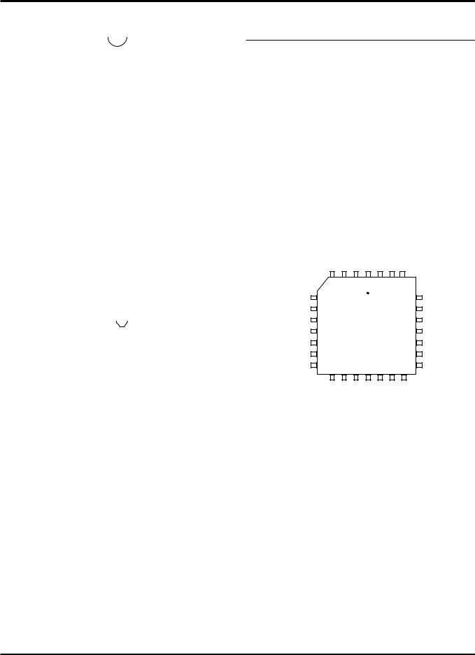
In/Output |
35-39 P20-24 |
Port 2, Pin 0,1,2,3,4 |
In/Output |
|
40 |
/DS |
Data Strobe |
Output |
|
|
|
|
4 |
CP96DZ82900 |

|
|
|
|
|
|
|
|
|
|
|
|
|
|
|
|
|
|
|
|
|
|
|
|
|
|
|
|
|
|
Z86C30/C31/C32/C40 |
ZILOG |
|
|
|
|
|
|
|
|
|
|
|
|
|
|
|
|
|
|
|
|
|
|
|
|
|
|
|
CP96DZ82900 |
||
PIN DESCRIPTION (Continued) |
|
|
|
|
|
|
|
|
|
|
|
|
|
|
|
|
|
|
|
|
|
|
|
|
|
|
|
|
||
|
|
|
|
|
P20 |
|
P03 |
|
P13 |
|
P12 |
|
GND |
|
GND |
|
P02 |
P11 |
|
P10 |
P01 |
P00 |
|
|
||||||
|
|
|
|
|
|
|
|
|
|
|
|
|
|
|
|
|
|
|
|
|
|
|
|
|
|
|
|
|
|
|
|
|
|
|
|
|
|
|
|
|
|
|
|
|
|
|
|
|
|
|
|
|
|
|
|
|
|
|
|
|
|
|
|
|
6 |
5 |
4 |
3 |
2 |
1 |
44 |
43 |
42 |
41 40 |
|
|
|
|
||||||||||||||
|
|
|
|
|
|
|
||||||||||||||||||||||||
P21 |
|
|
7 |
|
|
|
|
|
|
|
|
|
|
|
|
|
|
|
|
|
|
|
|
|
39 |
|
P30 |
|||
|
|
|
|
|
|
|
|
|
|
|
|
|
|
|
|
|
|
|
|
|
|
|
|
|||||||
P22 |
|
|
8 |
|
|
|
|
|
|
|
|
|
|
|
|
|
|
|
|
|
|
|
|
|
38 |
|
P36 |
|||
|
|
|
|
|
|
|
|
|
|
|
|
|
|
|
|
|
|
|
|
|
|
|
||||||||
P23 |
|
|
9 |
|
|
|
|
|
|
|
|
|
|
|
|
|
|
|
|
|
|
|
|
|
37 |
|
P37 |
|||
|
|
|
|
|
|
|
|
|
|
|
|
|
|
|
|
|
|
|
|
|
|
|
||||||||
P24 |
|
|
10 |
|
|
|
|
|
|
|
|
|
|
|
|
|
|
|
|
|
|
|
|
|
36 |
|
P35 |
|||
|
|
|
|
|
|
|
|
|
|
|
|
|
|
|
|
|
|
|
|
|
|
|
|
|||||||
/DS |
|
|
11 |
|
|
|
|
|
|
|
Z86C40 |
|
|
|
|
|
|
|
35 |
|
/RESET |
|||||||||
|
|
|
|
|
|
|
|
|
|
|
|
|
|
|
|
|||||||||||||||
N/C |
|
|
12 |
|
|
|
|
|
|
|
|
|
|
|
|
|
|
34 |
|
R//RL |
||||||||||
|
|
|
|
|
|
|
|
|
|
|
|
|
|
|
|
|
||||||||||||||
R//W |
|
|
13 |
|
|
|
|
|
|
|
|
|
|
|
|
|
|
|
|
|
|
|
|
|
33 |
|
/AS |
|||
|
|
|
|
|
|
|
|
|
|
|
|
|
|
|
|
|
|
|
|
|
|
|
||||||||
P25 |
|
|
14 |
|
|
|
|
|
|
|
|
|
|
|
|
|
|
|
|
|
|
|
|
|
32 |
|
P34 |
|||
|
|
|
|
|
|
|
|
|
|
|
|
|
|
|
|
|
|
|
|
|
|
|
|
|||||||
P26 |
|
|
15 |
|
|
|
|
|
|
|
|
|
|
|
|
|
|
|
|
|
|
|
|
|
31 |
|
P33 |
|||
|
|
|
|
|
|
|
|
|
|
|
|
|
|
|
|
|
|
|
|
|
|
|
||||||||
P27 |
|
|
16 |
|
|
|
|
|
|
|
|
|
|
|
|
|
|
|
|
|
|
|
|
|
30 |
|
P32 |
|||
|
|
|
|
|
|
|
|
|
|
|
|
|
|
|
|
|
|
|
|
|
|
|
|
|||||||
P04 |
|
|
17 |
|
|
|
|
|
|
|
|
|
|
|
|
|
|
|
|
|
|
|
|
|
29 |
|
P31 |
|||
|
|
|
|
|
|
|
|
|
|
|
|
|
|
|
|
|
|
|
|
|
|
|
|
|||||||
|
|
|
18 |
19 |
20 |
21 |
22 |
23 |
24 |
25 |
26 |
27 |
28 |
|
|
|
||||||||||||||
|
|
|
|
|
|
|
|
|
|
|
|
|
|
|
|
|
|
|
|
|
|
|
|
|
|
|
|
|
|
|
|
|
|
|
|
|
|
|
|
|
|
|
|
|
|
|
|
|
|
|
|
|
|
|
|
|
|
|
|
|
|
|
|
|
|
P05 |
P06 |
P14 |
|
P15 |
P07 |
|
VCC |
|
VCC |
P16 |
|
P17 |
XTAL2 |
XTAL1 |
|
|
||||||||||
44-Pin PLCC Pin Assignments
|
44-Pin PLCC Pin Identification |
|
||
Pin # Symbol Function |
Direction |
|
Pin # Symbol Function |
Direction |
1-2 |
GND |
Ground, GND |
|
3-4 |
P12-13 |
Port 1, Pins 2,3 |
In/Output |
5 |
P03 |
Port 0, Pin 3 |
In/Output |
6-10 |
P20-24 |
Port 2, Pins 0,1,2,3,4 |
In/Output |
11 |
/DS |
Data Strobe |
Output |
|
|
|
|
12 |
N/C |
Not Connected |
|
13 |
R//W |
Read/Write |
Output |
14-16 |
P25-27 |
Port 2, Pins 5,6,7 |
In/Output |
17-19 |
P04-06 |
Port 0, Pins 4,5,6 |
In/Output |
20-21 |
P14-15 |
Port 1, Pins 4,5 |
In/Output |
|
|
|
|
22 |
P07 |
Port 0, Pin 7 |
In/Output |
23-24 |
VCC |
Power Supply |
In/Output |
25-26 |
P16-17 |
Port 1, Pins 6,7 |
|
27 |
XTAL2 |
Crystal, Oscillator Clock |
Output |
|
|
|
|
28 |
XTAL1 |
Crystal, Oscillator Clock |
Input |
29-31 P31-33 |
Port 3, Pins 1,2,3 |
Input |
|
32 |
P34 |
Port 3, Pin 4 |
Output |
33 |
/AS |
Address Strobe |
Output |
34 |
R//RL |
ROM/ROMless Control |
Input |
|
|
|
|
35 |
/RESET |
Reset |
Input |
36 |
P35 |
Port 3, Pin 5 |
Output |
37 |
P37 |
Port 3, Pin 7 |
Output |
38 |
P36 |
Port 3, Pin 6 |
Output |
39 |
P30 |
Port 3, Pin 0 |
Input |
|
|
|
|
40-41 P00-01 |
Port 0, Pins 0,1 |
In/Output |
|
42-43 P10-11 |
Port 1, Pins 0,1 |
In/Output |
|
44 |
P02 |
Port 0, Pin 2 |
In/Output |
|
|
|
|
CP96DZ82900 |
5 |
ZILOG |
Z86C30/C31/C32/C40 |
CP96DZ82900 |
PIN DESCRIPTION (Continued)
|
|
|
|
|
|
|
P20 |
|
P03 |
|
P13 |
|
P12 |
|
GND |
|
GND |
|
P02 |
|
P11 |
|
P10 |
|
P01 |
|
P00 |
|
|
|
|
||||||||||||
|
|
|
|
|
|
|
|
|
|
|
|
|
|
|
|
|
|
|
|||||||||||||||||||||||||
|
|
|
|
|
|
|
|
|
|
|
|
|
|
|
|
|
|
|
|
|
|
|
|
|
|
|
|
|
|
|
|
|
|
|
|
|
|
|
|
|
|
|
|
|
|
|
|
|
|
|
|
|
|
|
|
|
|
|
|
|
|
|
|
|
|
|
|
|
|
|
|
|
|
|
|
|
|
|
|
|
|
|
|
|
|
|
|
|
|
|
|
|
|
|
|
|
|
|
|
|
|
|
|
|
|
|
|
|
|
|
|
|
|
|
|
|
|
|
|
|
|
|
|
|
|
|
|
|
|||
P21 |
|
|
33 |
32 |
31 |
30 |
29 |
28 |
27 |
26 |
25 |
24 |
23 |
|
|
|
|
|
|||||||||||||||||||||||||
|
|
|
|
|
|
||||||||||||||||||||||||||||||||||||||
|
|
|
|
34 |
|
|
|
|
|
|
|
|
|
|
|
|
|
|
|
|
|
|
|
|
|
|
|
|
|
|
|
|
|
22 |
|
|
|
P30 |
|||||
P22 |
|
|
|
|
35 |
|
|
|
|
|
|
|
|
|
|
|
|
|
|
|
|
|
|
|
|
|
|
|
|
|
|
|
|
|
21 |
|
|
|
P36 |
||||
P23 |
|
|
|
|
36 |
|
|
|
|
|
|
|
|
|
|
|
|
|
|
|
|
|
|
|
|
|
|
|
|
|
|
|
|
|
20 |
|
|
|
P37 |
||||
|
|
|
|
|
|
|
|
|
|
|
|
|
|
|
|
|
|
|
|
|
|
|
|
|
|
|
|
|
|
|
|
|
|
||||||||||
P24 |
|
|
|
|
37 |
|
|
|
|
|
|
|
|
|
|
|
|
|
|
|
|
|
|
|
|
|
|
|
|
|
|
|
|
|
19 |
|
|
|
P35 |
||||
/DS |
|
|
|
|
38 |
|
|
|
|
|
|
|
|
|
|
|
|
|
|
|
|
|
|
|
|
|
|
|
|
|
|
|
|
|
|
|
|
||||||
|
|
|
|
|
|
|
|
|
|
|
|
|
|
|
Z86C40 |
|
|
|
|
|
|
|
|
|
18 |
|
|
|
/RESET |
||||||||||||||
N/C |
|
|
|
|
39 |
|
|
|
|
|
|
|
|
|
|
|
|
|
|
|
|
|
|
|
|
17 |
|
|
|
R//RL |
|||||||||||||
R//W |
|
|
|
|
40 |
|
|
|
|
|
|
|
|
|
|
|
|
|
|
|
|
|
|
|
|
|
|
|
|
|
|
|
|
|
16 |
|
|
|
/AS |
||||
P25 |
|
|
|
|
41 |
|
|
|
|
|
|
|
|
|
|
|
|
|
|
|
|
|
|
|
|
|
|
|
|
|
|
|
|
|
15 |
|
|
|
P34 |
||||
P26 |
|
|
|
|
42 |
|
|
|
|
|
|
|
|
|
|
|
|
|
|
|
|
|
|
|
|
|
|
|
|
|
|
|
|
|
14 |
|
|
|
P33 |
||||
P27 |
|
|
|
|
43 |
|
|
|
|
|
|
|
|
|
|
|
|
|
|
|
|
|
|
|
|
|
|
|
|
|
|
|
|
|
13 |
|
|
|
P32 |
||||
P04 |
|
|
|
|
44 |
|
|
|
|
|
|
|
|
|
|
|
|
|
|
|
|
|
|
|
|
|
|
|
|
|
|
|
|
|
12 |
|
|
|
P31 |
||||
|
|
|
1 |
|
2 |
|
3 |
|
4 |
|
5 |
|
6 |
|
7 |
|
8 |
|
9 |
|
10 |
11 |
|
|
|
|
|
|
|||||||||||||||
|
|
|
|
|
|
|
|
|
|
|
|
|
|
|
|
|
|||||||||||||||||||||||||||
|
|
|
|
|
|
|
|
|
|
|
|
|
|
|
|
|
|
|
|
|
|
|
|
|
|
|
|
|
|
|
|
|
|
|
|
|
|
|
|
|
|
|
|
|
|
|
|
|
|
|
|
|
|
|
|
|
|
|
|
|
|
|
|
|
|
|
|
|
|
|
|
|
|
|
|
|
|
|
|
|
|
|
|
|
|
|
|
|
|
|
|
|
|
|
|
|
|
|
|
|
|
|
|
|
|
|
|
|
|
|
|
|
|
|
|
|
|
|
|
|
|
|
|
|
|
|
|
|
|
|
|
|
|
|
|
|
|
|
|
|
|
|
|
|
|
|
|
|
|
|
|
|
|
|
|
|
|
|
|
|
|
|
|
|
|
|
|
|
|
|
|
|
|
|
|
|
|
|
|
|
|
P05 |
P06 |
P14 |
P15 |
|
P07 |
|
VCC |
|
VCC |
|
P16 |
|
P17 |
|
XTAL2 |
|
XTAL1 |
|
|
|
|
||||||||||||||||
44-Pin QFP Pin Assignments
|
44-Pin QFP Pin Identification |
|
|
Pin # Symbol Function |
Direction |
Pin # Symbol Function |
Direction |
1-2 |
P05-06 |
Port 0, Pins 5,6 |
In/Output |
3-4 |
P14-15 |
Port 1, Pins 4,5 |
In/Output |
5 |
P07 |
Port 0, Pin 7 |
In/Output |
6-7 |
VCC |
Power Supply |
In/Output |
8-9 |
P16-17 |
Port 1 Pins 6,7 |
|
|
|
|
|
10 |
XTAL2 |
Crystal, Oscillator Clock |
Output |
11 |
XTAL1 |
Crystal, Oscillator Clock |
Input |
12-14 P31-33 |
Port 3, Pins 1,2,3 |
Input |
|
15 |
P34 |
Port 3, Pin 4 |
Output |
16 |
/AS |
Address Strobe |
Output |
|
|
|
|
17 |
R//RL |
ROM/ROMless Control |
Input |
18 |
/RESET |
Reset |
Input |
19 |
P35 |
Port 3, Pin 5 |
Output |
20 |
P37 |
Port 3, Pin 7 |
Output |
|
|
|
|
21 |
P36 |
Port 3, Pin 6 |
Output |
22 |
P30 |
Port 3, Pin 0 |
Input |
23-24 P00-01 |
Port 0, Pins 0,1 |
In/Output |
|
25-26 P10-11 |
Port 1, Pins 0,1 |
In/Output |
|
27 |
P02 |
Port 0, Pin 2 |
In/Output |
|
|
|
|
28-29 |
GND |
Ground, GND |
|
30-31 P12-13 |
Port 1, Pins 2,3 |
In/Output |
|
32 |
P03 |
Port 0, Pin 3 |
In/Output |
33-37 P20-24 |
Port 2, Pins 0,1,2,3,4 |
In/Output |
|
38 |
/DS |
Data Strobe |
Output |
|
|
|
|
39 |
N/C |
Not Connected |
|
40 |
R//W |
Read/Write |
Output |
41-43 P25-27 |
Port 2, Pins 5,6,7 |
In/Output |
|
44 |
P04 |
Port 0, Pin 4 |
In/Output |
|
|
|
|
6 |
CP96DZ82900 |
 Loading...