


ZILOG Z86C9008VSC, Z86C9012FSC, Z86C9012PSC, Z86C9012VSC, Z86C8912FEC Datasheet
...CUSTOMER PROCUREMENT SPECIFICATION
Z86C90/C89
ROMLESS CMOS
Z8® 8-BIT MICROCONTROLLER
GENERAL DESCRIPTION
The Z86C90/C89 CCP™ (Consumer Controller Processor) introduces a new level of sophistication to single-chip architecture. The Z86C90/C89 are ROMless members of the Z8 single-chip microcontroller family with 236 bytes of general purpose RAM. The only difference that exists between the Z86C89 and the Z86C90 is that the on-chip oscillator of the Z86C89 can accept an external RC network or other external clock source, while the Z86C90's on-chip oscillator accepts a crystal, ceramic resonator, LC, or external clock source drive. The CCP controllers are housed in a 40-pin DIP, 44-pin Leaded Chip Carrier, or a 44-pin Quad Flat Pack, and are CMOS compatible. The CCP offers the use of external memory which enables this Z8 microcomputer to be used where code flexibility is required. Zilog's CMOS microcomputer offers fast execution, efficient use of memory, sophisticated interrupts, input/output bit manipulation capabilities, and easy hardware/software system expansion along with low cost and low power consumption.
The Z86C90/C89 architecture is based on Zilog's 8-bit microcontroller core with an Expanded Register File to allow access to register mapped peripheral and I/O circuits. The CCP offers a flexible I/O scheme, an efficient register and address space structure, and a number of ancillary features that are useful in many industrial, automotive, computer peripherals, and advanced scientific applications.
The CCP applications demand powerful I/O capabilities. The Z86C90/C89 fulfills this with 32 pins dedicated to input and output. These lines are grouped into four ports. Each port consists of eight lines, and is configurable under software control to provide timing, status signals, parallel I/O with or without handshake, and an address/data bus for interfacing external memory.
There are four basic address spaces available to support this wide range of configurations: Program Memory, Register File, Data Memory, and Expanded Register File. The Register File is composed of 236 bytes of general purpose registers, four I/O port registers, and fifteen control and status registers. The Expanded Register File consists of two control registers.
To unburden the program from coping with the real-time problems, such as counting/timing and data communication, the Z86C90/C89 offers two on-chip counter/timers. Included are a large number of user selectable modes, and two on-board comparators to process analog signals with a common reference voltage (see Functional Block Diagram).
Notes:
All Signals with a preceding front slash, "/", are active Low, e.g.: B//W (WORD is active Low); /B/W (BYTE is active Low, only).
Power connections follow conventional descriptions below:
Connection |
Circuit |
Device |
|
|
|
Power |
VCC |
VDD |
Ground |
GND |
VSS |
DC-4054-01 |
(10-17-91) |
1 |

GENERAL DESCRIPTION (Continued)
Output Input
Port 3
Counter/
Timers (2)
Interrupt
Control
Two Analog
Comparators 
Port 2
I/O
(Bit Programmable)
Vcc GND
ALU
FLAGS
Register
Pointer
Register File
256 x 8-Bit
Port 0
4 4
Address or I/O (Nibble Programmable)
XTAL /AS /DS R//W /RESET
Machine Timing
&
Instruction Control
RESET
WDT, POR
Program
Counter
Port 1
8
Address/Data or I/O (Byte Programmable)
Functional Block Diagram
2

PIN DESCRIPTION
R//W |
|
1 |
|
40 |
|
/DS |
|
|
|
||||
P25 |
|
2 |
|
39 |
|
P24 |
|
|
|
||||
P26 |
|
3 |
|
38 |
|
P23 |
|
|
|
||||
P27 |
|
4 |
|
37 |
|
P22 |
|
|
|
||||
P04 |
|
5 |
|
36 |
|
P21 |
|
|
|
||||
P05 |
|
6 |
|
35 |
|
P20 |
|
|
|
||||
P06 |
|
7 |
|
34 |
|
P03 |
|
|
|
||||
P14 |
|
8 |
|
33 |
|
P13 |
|
|
|
||||
P15 |
|
9 |
Z86C90/C89 |
32 |
|
P12 |
|
|
|||||
P07 |
|
10 |
31 |
|
GND |
|
|
DIP |
|
||||
VCC |
|
11 |
|
30 |
|
P02 |
|
|
|
||||
|
|
|||||
P16 |
|
12 |
|
29 |
|
P11 |
|
|
|
||||
|
|
|||||
P17 |
|
13 |
|
28 |
|
P10 |
|
|
|
||||
|
|
|||||
XTAL2 |
|
14 |
|
27 |
|
P01 |
|
|
|
||||
|
|
|||||
XTAL1 |
|
15 |
|
26 |
|
P00 |
|
|
|
||||
P31 |
|
16 |
|
25 |
|
P30 |
|
|
|
||||
P32 |
|
17 |
|
24 |
|
P36 |
|
|
|
||||
P33 |
|
18 |
|
23 |
|
P37 |
|
|
|
||||
P34 |
|
19 |
|
22 |
|
P35 |
|
|
|
||||
/AS |
|
20 |
|
21 |
|
/RESET |
|
|
|
||||
|
|
|
|
|
|
|
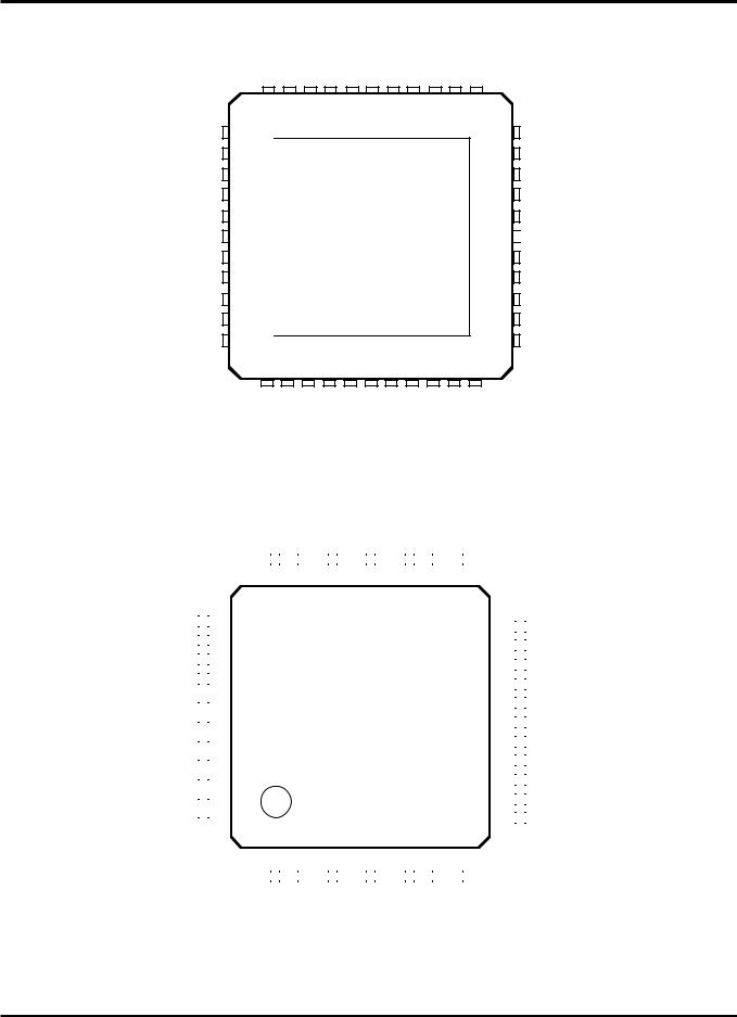
40-Pin DIP Pin Assignments
3
PIN DESCRIPTION (Continued)
|
P20 |
P03 |
P13 |
P12 |
GND |
GND |
P02 |
P11 |
P10 |
P01 |
|
6 |
5 |
4 |
3 |
2 |
1 |
44 |
43 |
42 |
41 |
P21 |
7 |
|
|
|
|
|
|
|
|
|
P22 |
8 |
|
|
|
|
|
|
|
|
|
P23 |
9 |
|
|
|
|
|
|
|
|
|
P24 |
10 |
|
|
|
|
|
|
|
|
|
/DS |
11 |
|
|
Z86C90/C89 |
|
|
||||
N/C |
12 |
|
|
|
|
|||||
|
|
|
PLCC |
|
|
|
||||
|
|
|
|
|
|
|
|
|||
R//W |
13 |
|
|
|
|
|
|
|
|
|
P25 |
14 |
|
|
|
|
|
|
|
|
|
P26 |
15 |
|
|
|
|
|
|
|
|
|
P27 |
16 |
|
|
|
|
|
|
|
|
|
P04 |
17 |
|
|
|
|
|
|
|
|
|
|
|
|
|
|
|
|
|
|
||
|
18 |
19 |
20 |
21 |
22 |
23 |
24 |
25 |
26 |
27 |
|
P05 |
P06 |
P14 |
P15 |
P07 |
VCC |
VCC |
P16 |
P17 |
XTAL2 |
P00
40
39 P30
38 P36
37 P37
36 P35
35 /RESET
34 
 GND
GND
33 /AS
32 P34
31 P33
30 P32
29 P31
28 XTAL1
44-Pin PLCC Pin Assignments
P20 |
|
P03 |
|
P13 |
|
|
|
|
|
|
|
|
|
|
|
|
|
|
|
|
|
|
|
|
33 32 31
P21 |
|
|
|
34 |
P22 |
|
35 |
||
|
|
|
||
P23 |
|
36 |
||
|
|
|
||
P24 |
|
37 |
||
|
|
|
||
/DS |
|
38 |
||
|
|
|
||
N/C |
|
39 |
||
|
|
|
||
R//W |
|
40 |
||
|
|
|
||
P25 |
|
41 |
||
|
|
|
||
P26 |
|
42 |
||
|
|
|
||
P27 |
|
43 |
||
|
|
|
||
P04 |
|
44 |
||
|
|
|
||
1 |
2 |
3 |
||
|
|
|
|
|
|
|
|
|
|
|
|
|
|
|
|
|
|
|
|
P05 |
|
P06 |
|
P14 |
P12 |
GND |
GND |
P02 |
|
|
P11 |
|
P10 |
|
P01 |
|
|
P00 |
|
|
|
|
|||||||||||||
|
|
|
|
|
|
|
|
|
|
|
||||||||||||||||||||
|
|
|
|
|
|
|
|
|
|
|
|
|
|
|
|
|
|
|
|
|
|
|
|
|
|
|
|
|
|
|
|
|
|
|
|
|
|
|
|
|
|
|
|
|
|
|
|
|
|
|
|
|
|
|
|
|
|
|
|
|
|
|
|
|
|
|
|
|
|
|
|
|
|
|
|
|
|
|
|
|
|
|
|
|
|
|
|
|
|
|
|
|
30 |
29 |
28 27 |
26 |
25 |
24 |
23 |
|
|
|
|
||||||||||||||||||||
|
|
|
|
|
|
|
|
|
|
|
|
|
|
|
|
|
|
|
|
|
|
|
22 |
|
|
|
P30 |
|||
|
|
|
|
|
|
|
|
|
|
|
|
|
|
|
|
|
|
|
|
|
|
|
|
|
|
|||||
|
|
|
|
|
|
|
|
|
|
|
|
|
|
|
|
|
|
|
|
|
|
|
21 |
|
|
|
P36 |
|||
|
|
|
|
|
|
|
|
|
|
|
|
|
|
|
|
|
|
|
|
|
|
|
|
|
|
|||||
|
|
|
|
|
|
|
|
|
|
|
|
|
|
|
|
|
|
|
|
|
|
|
20 |
|
|
|
P37 |
|||
|
|
|
|
|
|
|
|
|
|
|
|
|
|
|
|
|
|
|
|
|
|
|
|
|
|
|||||
Z86C90/C89 |
|
|
|
|
|
|
19 |
|
|
|
P35 |
|||||||||||||||||||
|
|
|
|
|
|
|
|
|
||||||||||||||||||||||
|
|
|
|
|
|
18 |
|
|
|
/RESET |
||||||||||||||||||||
|
|
|
|
|
|
|
|
|
||||||||||||||||||||||
|
|
|
|
|
|
|
|
|
||||||||||||||||||||||
|
|
|
|
QFP |
|
|
|
|
|
|
|
|
|
|
|
|
17 |
|
|
|
GND |
|||||||||
|
|
|
|
|
|
|
|
|
|
|
|
|
|
|
|
|
|
|||||||||||||
|
|
|
|
|
|
|
|
|
|
|
|
|
|
|
|
|
|
|
|
|
|
|
16 |
|
|
|
/AS |
|||
|
|
|
|
|
|
|
|
|
|
|
|
|
|
|
|
|
|
|
|
|
|
|
|
|
|
|||||
|
|
|
|
|
|
|
|
|
|
|
|
|
|
|
|
|
|
|
|
|
|
|
15 |
|
|
|
P34 |
|||
|
|
|
|
|
|
|
|
|
|
|
|
|
|
|
|
|
|
|
|
|
|
|
|
|
|
|||||
|
|
|
|
|
|
|
|
|
|
|
|
|
|
|
|
|
|
|
|
|
|
|
14 |
|
|
|
P33 |
|||
|
|
|
|
|
|
|
|
|
|
|
|
|
|
|
|
|
|
|
|
|
|
|
|
|
|
|||||
|
|
|
|
|
|
|
|
|
|
|
|
|
|
|
|
|
|
|
|
|
|
|
13 |
|
|
|
P32 |
|||
|
|
|
|
|
|
|
|
|
|
|
|
|
|
|
|
|
|
|
|
|
|
|
|
|
|
|||||
|
|
|
|
|
|
|
|
|
|
|
|
|
|
|
|
|
|
|
|
|
|
|
12 |
|
|
|
P31 |
|||
|
|
|
|
|
|
|
|
|
|
|
|
|
|
|
|
|
|
|
|
|
|
|
|
|
|
|||||
4 |
|
|
5 |
|
|
6 |
|
7 |
|
8 |
|
9 |
|
10 |
11 |
|
|
|
|
|||||||||||
|
|
|
|
|
|
|
|
|
|
|
|
|
|
|
|
|
|
|
|
|
|
|
|
|
|
|
|
|
|
|
|
|
|
|
|
|
|
|
|
|
|
|
|
|
|
|
|
|
|
|
|
|
|
|
|
|
|
|
|
|
|
|
|
|
|
|
|
|
|
|
|
|
|
|
|
|
|
|
|
|
|
|
|
|
|
|
|
|
|
|
|
|
|
|
|
|
|
|
|
|
|
|
|
|
|
|
|
|
|
|
|
|
|
|
|
|
|
|
|
|
|
|
|
P15 |
|
P07 |
VCC |
VCC |
|
|
P16 |
|
P17 |
|
XTAL2 |
XTAL1 |
|
|
|
|
||||||||||||||
44-Pin QFP Pin Assignments
4
STANDARD TEST CONDITIONS
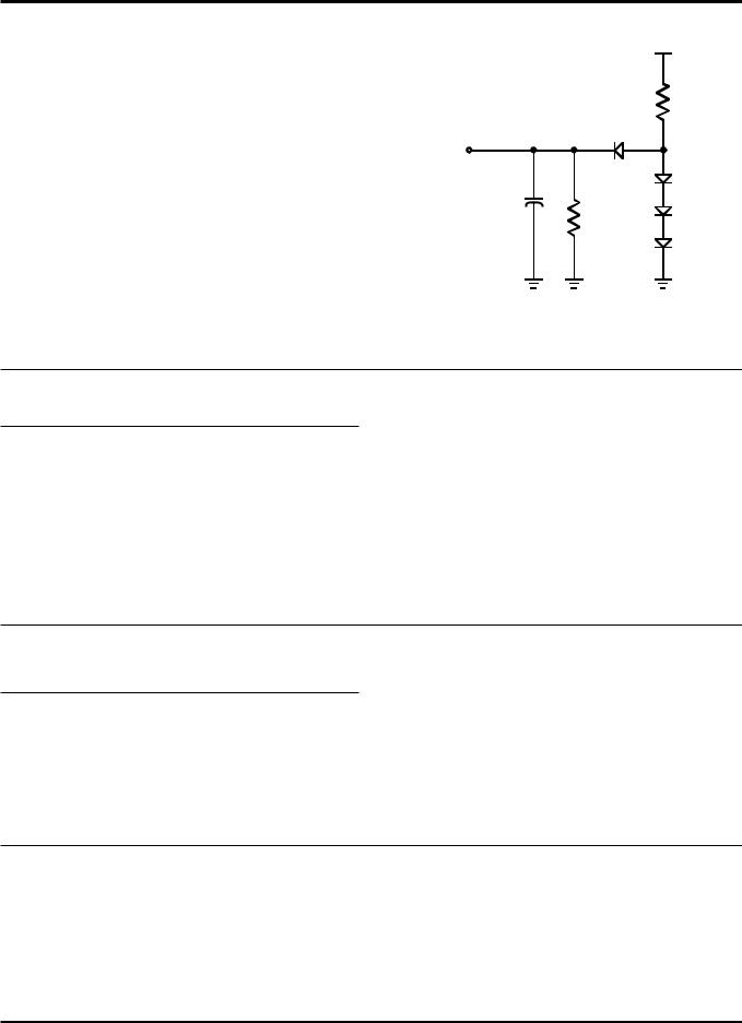
The characteristics listed below apply for standard test conditions as noted. All voltages are referenced to GND. Positive current flows into the referenced pin (Test Load Diagram).
+5V
2.1 KΩ
From Output
Under Test
150 pF
9.1 KΩ
Test Load Diagram
ABSOLUTE MAXIMUM RATINGS
Symbol |
Description |
Min |
Max |
Units |
|
|
|
|
|
VCC |
Supply Voltage (*) |
-0.3 |
+7.0 |
V |
TSTG |
Storage Temp |
-65° |
+150° |
C |
TA |
Oper Ambient Temp |
|
† |
C |
|
Power Dissipation |
|
2.2 |
W |
|
|
|
|
|
Notes:* Voltage on all pins with respect to GND.
† See Ordering Information.
ings may cause permanent damage to the device. This is a stress rating only; operation of the device at any condition above those indicated in the operational sections of these specifications is not implied. Exposure to absolute maximum rating conditions for an e x t e n d e d period may affect device reliability.
Stress greater than those listed under Absolute Maximum Rat-
CAPACITANCE
TA = 25°C, VCC = GND = 0V, f = 1.0 MHz, unmeasured pins to GND
Parameter |
Max |
|
|
Input capacitance |
12 pF |
Output capacitance |
12 pF |
I/O capacitance |
12 pF |
|
|
PLEASE NOTE
These devices will not operate in extended timing mode. Set Register 248, D5 = 0.
5
 Loading...