


Z86C7116PSC
ZILOG Z86C7116PSC, Z86L7008PSC, Z86L7008SSC, Z86L7108PSC, Z86L7108SSC Datasheet
...
DS97LVO0500
P R E L I M I N A R Y
1-1
1
P
RELIMINARY
P
RODUCT
S
PECIFICATION
Z86L70/71/75/C71
1
IR/L
OW
-V
OLTAGE
M
ICROCONTROLLER
FEATURES
■
Two Standby Modes (Typical)
– STOP - 2
µ
A
– HALT - 0.8 mA
■
Special Architecture to Automate Both Generation and
Reception of Complex Pulses or Signals:
– One Programmable 8-Bit Counter/Timer with Two
Capture Registers
– One Programmable 16-Bit Counter/Timer with
One Capture Register
– Programmable Input Glitch Filter for Pulse
Reception
■
Five Priority Interrupts
■
Low Voltage Detection and Protection
■
Programmable Watch-Dog/Power-On Reset Circuits
■
Two Independent Comparators with Programmable
Interrupt Polarity
■
On-Chip Oscillator that Accepts a Crystal, Ceramic
Resonator, LC, RC (mask option), or External Clock
Drive
■
Mask Selectable 200 KOhm Pull-Ups on Ports 0, 2, 3
GENERAL DESCRIPTION
The Z86L7X family of IR (Infrared)/Low-Voltage Microcon-
trollers are ROM/ROMless-based members of the Z8
®
MCU
single-chip family with 237/125 bytes of internal
RAM. The differentiating factor between these devices is
the availability of RAM, ROM and package options. Offer-
ing the 3V versions (Z86LXX) with the Z86C71 gives opti-
mum performance in both the low and high voltage ranges.
Zilog's CMOS Low-Voltage Microcontrollers offer fast exe-
cution, efficient use of memory, sophisticated interrupts, in-
put/output bit manipulation capabilities, automated pulse
generation/reception, and internal key-scan pull-up resis-
tors. The Z86L7X product line offers easy hardware/soft-
ware system expansion with cost-effective and low power
consumption.
The Z86L7X architecture is based on Zilog's 8-bit micro-
controller core with an Expanded Register File to allow ac-
cess to register mapped peripherals, I/O circuits, and pow-
erful counter/timer circuitry. The Z8
MCU offers a flexible
I/O scheme, an efficient register and address space struc-
ture, and a number of ancillary features that are useful in
many consumer, automotive, computer peripheral, and
battery operated hand-held applications.
There are three basic address spaces available to support
a wide range of configurations: Program Memory, Register
File, and Expanded Register File. The register file is com-
posed of 256/144 bytes of RAM. It includes four I/O port
registers, 15 control and status registers and the rest are
General-Purpose registers. The Expanded Register File
consists of two additional register groups (F and D). Exter-
nal Memory is not available on 18 and 20-pin versions.
Part
ROM
(KB)
RAM*
(Bytes) I/O
Voltage
Ranges
Z86L70 2 125 14 2.0V to 3.9V
Z86L71 8 237 16 2.0V to 3.9V
Z86L75 4 237 14 2.0V to 3.9V
Z86C71 8 237 16 4.5V to 5.5V
Note:
*General-Purpose
Z86L70/71/75/C71
IR/Low-Voltage Microcontroller Zilog
1-2
P R E L I M I N A R Y
DS97LVO0500
GENERAL DESCRIPTION
(Continued)
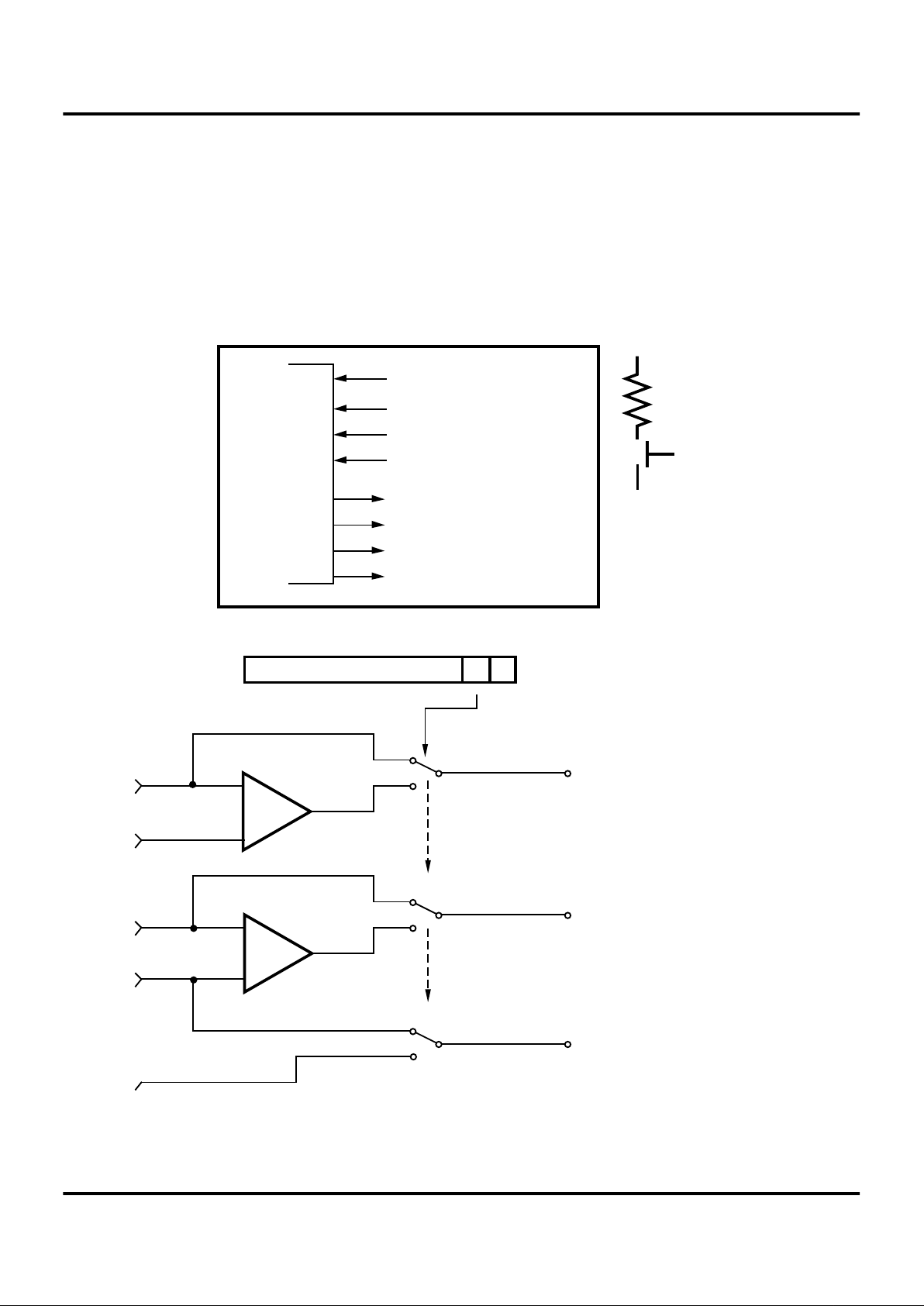
To unburden the program from coping with such real-time
problems as generating complex waveforms or receiving
and demodulating complex waveform/pulses, the Z86L7X
family offers a new intelligent counter/timer architecture
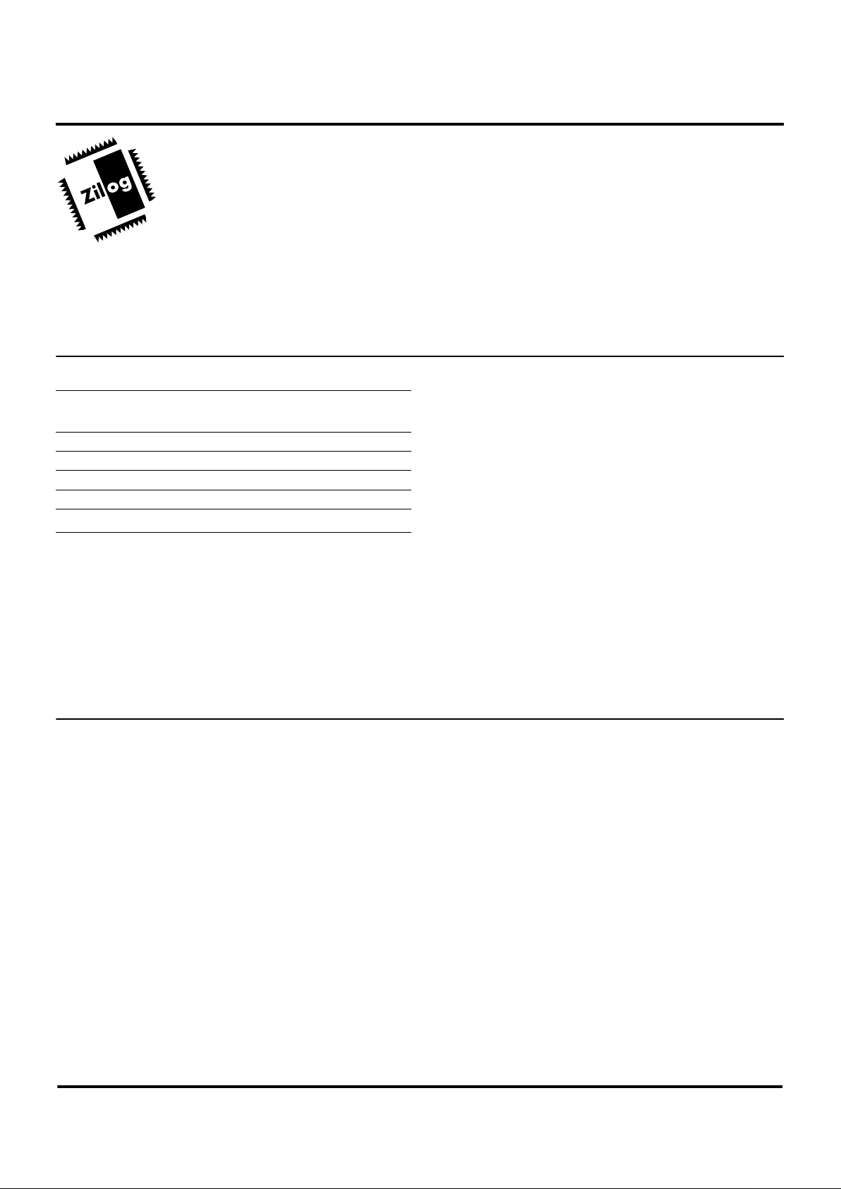
with 8-bit and 16-bit counter/timers (Figure 1). Also includ-
ed are a large number of user-selectable modes, and two
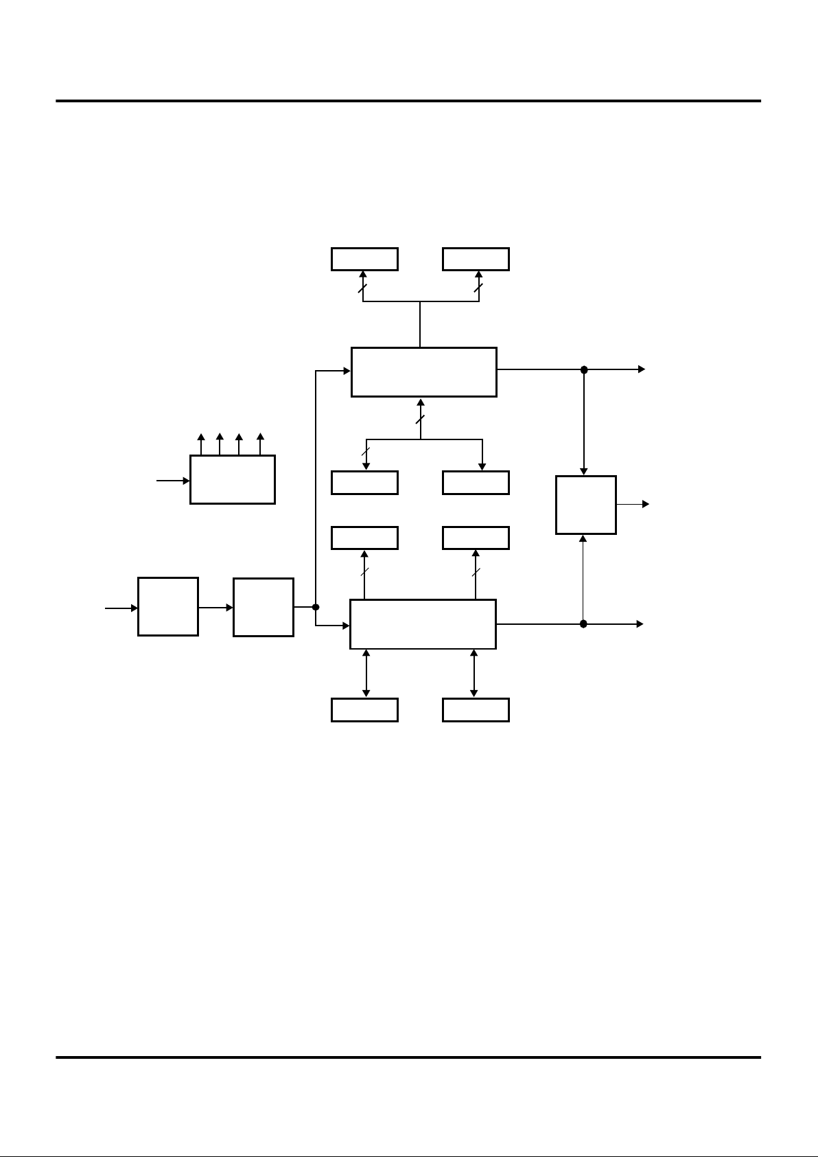
on-board comparators to process analog signals (Figure
2).
Figure 1. Counter/Timer Block Diagram
HI16
LO16
16-Bit
T16
TC16H
TC16L
HI8 LO8
And/Or
Logic
Clock
Divider
Glitch
Filter
Edge
Detect
Circuit
8-Bit
T8
TC8H
TC8L
8
8
16
8
Input
SCLK
1
2
48
Timer 16
Timer 8/16
Timer 8
8
8
8
8
8
Z86L70/71/75/C71
Zilog IR/Low-Voltage Microcontroller
DS97LVO0500
P R E L I M I N A R Y
1-3
1
Note:
All Signals with a preceding front slash, "/", are ac-
tive Low, for example, B//W (WORD is active Low); /B/W
(BYTE is active Low, only).
Power connections follow conventional descriptions be-
low:
Figure 2. Functional Block Diagram
Port 0
P00
P07
P31
P32
P33
Port 3
Register File
144/256 x 8-bit
ROM
2K/4K/8K x 8
Z8 Core
Register Bus
Internal
Address Bus
Internal Data Bus
Expanded
Register
File
Expanded
Register Bus
Counter/Timer 8
8-Bit
Counter/Timer 16
16-Bit
Power
VDD
VSS
P34
P35
P36
2
P20
P21
P22
P23
P24
P25
P26
P27
Port 2
I/O Bit
Programmable
Machine
Timing
&
Instruction
Control
XTAL2
XTAL1
Two Analog
Comparators
Interrupt Control
Connection Circuit Device
Power V
CC
V
DD
Ground GND V
SS
Z86L70/71/75/C71
IR/Low-Voltage Microcontroller Zilog
1-4
P R E L I M I N A R Y
DS97LVO0500
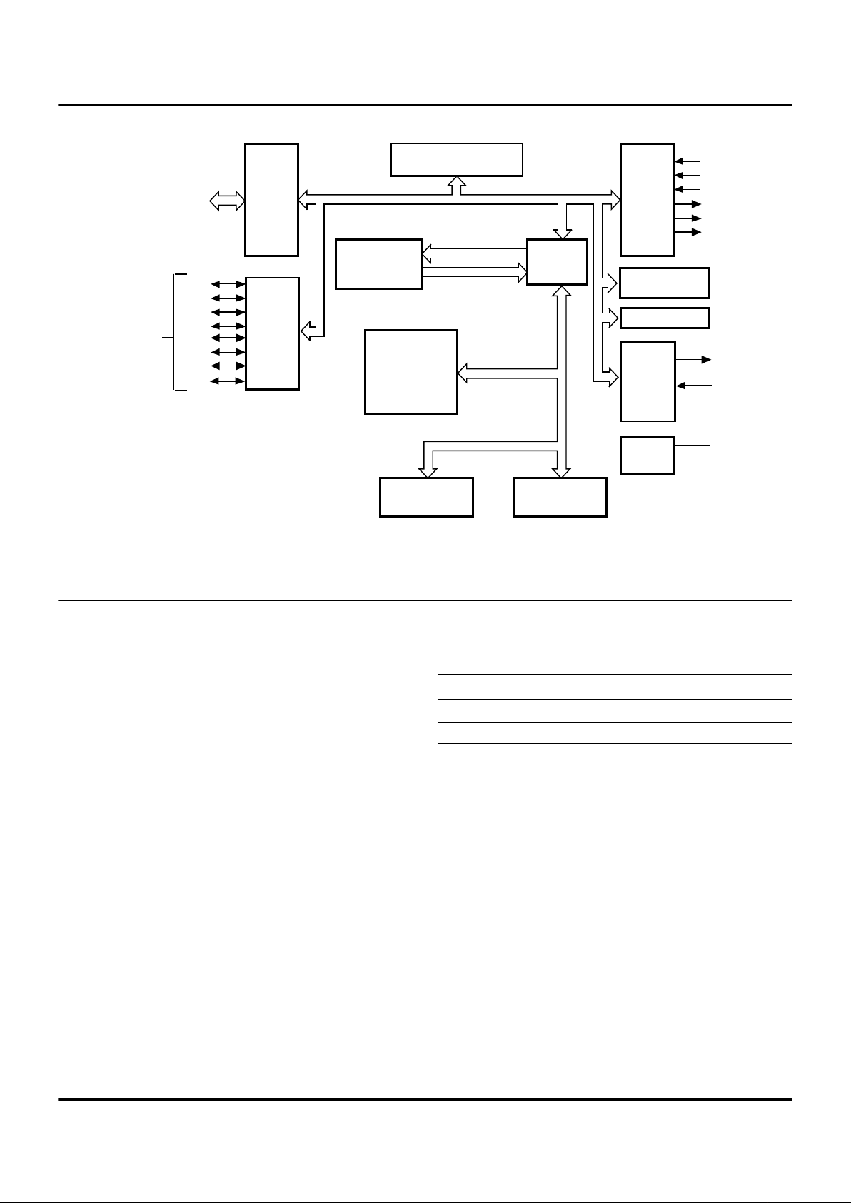
PIN DESCRIPTION
Figure 3. 18-Pin DIP/SOIC Pin Assignments
P24
P25
P26
P27
VDD
XTAL2
XTAL1
P31
P32
P23
P22
P21
P20
VSS
P36
P35
P34
P33
18
Z86L70/75
DIP/SOIC
1
910
Figure 4. 20-Pin DIP/SOIC Pin Assignments
P24
P25
P26
P27
VDD
XTAL2
XTAL1
P31
P32
P00
P23
P22
P21
P20
VSS
P36
P35
P34
P33
P07
20
Z86L71/C71
DIP/SOIC
1
10 11
Table 1. Pin Identification
20-Pin
DIP & SOIC
18-Pin DIP
& SOIC Symbol Direction Description
10
11
P00
P07
Input/Output
Input/Output
Port 0 pins are individually configurable as
input or output.
17
18
19
20
1
2
3
4
15
16
17
18
1
2
3
4
P20
P21
P22
P23
P24
P25
P26
P27
Input/Output
Input/Output
Input/Output
Input/Output
Input/Output
Input/Output
Input/Output
Input/Output
Port 2 pins are individually configurable as
input or output.
8
9
12
13
14
15
8
9
10
11
12
13
P31
P32
P33
P34
P35
P36
Input
Input
Input
Output
Output
Output
IRQ2/Modulator Input
IRQ0
IRQ1
T8 output
T16 output
T8/T16 output
7
6
5
16
7
6
5
14
XTAL1
XTAL2
V
DD
V
SS
Input
Output
Crystal, Oscillator Clock
Crystal, Oscillator Clock
Power Supply
Ground
Z86L70/71/75/C71
Zilog IR/Low-Voltage Microcontroller
DS97LVO0500
P R E L I M I N A R Y
1-5
1
ABSOLUTE MAXIMUM RATINGS
Stresses greater than those listed under Absolute Maxi-
mum Ratings may cause permanent damage to the de-
vice. This is a stress rating only; operation of the device at
any condition above those indicated in the operational sec-
tions of these specifications is not implied. Exposure to ab-
solute maximum rating conditions for an extended period
may affect device reliability.
STANDARD TEST CONDITIONS
The characteristics listed below apply for standard test
conditions as noted. All voltages are referenced to GND.
Positive current flows into the referenced pin (Figure 5).
CAPACITANCE
T
A
= 25
°
C, V
CC
= GND = 0V, f = 1.0 MHz, unmeasured pins returned to GND.
Symbol Description Min Max Units
V
CC
Supply V oltage (*) -0.3 +7.0 V
T
STG
Storage Temp. -65
°
+150
°
C
T
A
Oper. Ambient
Temp.
†C
Notes:
* Voltage on all pins with respect to GND.
† See Ordering Information
Figure 5. Test Load Diagram
From Output
Under Test
150 pFI
Parameter Max
Input capacitance 12 pF
Output capacitance 12 pF
I/O capacitance 12 pF

Z86L70/71/75/C71
IR/Low-Voltage Microcontroller Zilog
1-6
P R E L I M I N A R Y
DS97LVO0500
DC CHARACTERISTICS (Z86L70/71/75 LOW VOLTAGE SPECIFICATIONS)
Preliminary
T
A
= 0
°
C to +70
°
C
Typ @
Sym Parameter
V
CC
Min Max 25
°
C Units Conditions Notes
Max Input Voltage 2.0V
3.9V
7
7
V
V
I
IN
<250
µ
A
I
IN
<250
µ
A
V
CH
Clock Input
High Voltage
2.0V
3.9V
0.8 V
CC
0.8 V
CC
V
CC
+ 0.3
V
CC
+ 0.3
V
V
Driven by External
Clock Generator
Driven by External
Clock Generator
V
CL
Clock Input
Low V oltage
2.0V
3.9V
V
SS
– 0.3
V
SS
– 0.3
0.2 V
CC
0.2 V
CC
V
V
Driven by External
Clock Generator
Driven by External
Clock Generator
V
IH
Input High Voltage 2.0V
3.9V
0.7 V
CC
0.7 V
CC
V
CC
+ 0.3
V
CC
+ 0.3
0.5V
CC
0.5V
CC
V
V
V
IL
Input Low Voltage 2.0V
3.9V
V
SS
– 0.3
V
SS
– 0.3
0.2 V
CC
0.2 V
CC
0.5V
CC
0.5V
CC
V
V
V
OH1
Output High
Voltage
2.0V
3.9V
V
CC
– 0.4
V
CC
– 0.4
1.7
3.7
V
V
I
OH
= –0.5 mA
I
OH
= –0.5 mA
V
OH2
Output High
Voltage (P36,
P37,P00, P01)
2.0V
3.9V
V
CC
- 0.8
V
CC
- 0.8
V
V
I
OH
= –7 mA
I
OH
= –7 mA
V
OL1
Output Low
Voltage
2.0V
3.9V
0.4
0.4
0.1
0.2
V
V
I
OL
= 1.0 mA
I
OL
= 4.0 mA
V
OL2*
Output Low
Voltage
2.0V
3.9V
0.8
0.8
0.5
0.3
V
V
I
OL
= 5.0 mA
I
OL
= 7.0 mA
V
OL2
Output Low
Voltage(P36,
P37,P00,P01)
2.0V
3.9V
0.8
0.8
0.3
0.2
V
V
I
OL
= 10 mA
I
OL
= 10 mA
V
RH
Reset Input
High V oltage
2.0V
3.9V
0.8 V
CC
0.8 V
CC
V
CC
V
CC
1.5
2.0
V
V
V
Rl
Reset Input
Low V oltage
2.0V
3.9V
V
SS
– 0.3
V
SS
– 0.3
0.2 V
CC
0.2 V
CC
0.5
0.9
V
V
V
OFFSET
Comparator Input
Offset V oltage
2.0V
3.9V
25
25
10
10
mV
mV
I
IL
Input Leakage 2.0V
3.9V
-1
-1
1
1
< 1
< 1
µA
µA
V
IN
= O
V
, V
CC
V
IN
= O
V
, V
CC
I
OL
Output Leakage 2.0V
3.9V
–1
–1
1
1
< 1
< 1
µA
µA
V
IN
= O
V
, V
CC
V
IN
= O
V
, V
CC
I
IR
Reset Input Pull-
Up Current
2.0V
3.9V
–230
–400
-50
–90
µA
µA
V
IN
= O
V
V
IN
= O
V
I
CC
Supply Current 2.0V
3.9V
2.0V
3.9V
10
15
250
850
4
10
100
500
mA
mA
µA
µA
@ 8.0 MHz
@ 8.0 MHz
@ 32 kHz
@ 32 kHz
1,2
1,2
1,2,8

Z86L70/71/75/C71
Zilog IR/Low-Voltage Microcontroller
DS97LVO0500 P R E L I M I N A R Y 1-7
1
T
A
= 0°C to +70°C
Typ @
Sym Parameter
V
CC
Min Max 25°C Units Conditions Notes
I
CC1
Standby Current
(WDT Off)
2.0V
3.9V
3
5
1
4
mA
mA
HALT Mode
V
IN
= O
V
, V
CC
@
8.0 MHz
HALT Mode
V
IN
= O
V
, V
CC
@ 8.0 MHz
1,2
1,2
2.0V
3.9V
2
4
0.8
2.5
mA
mA
Clock Divide-by-
16 @ 8.0 MHz
Clock Divide-by-
16 @ 8.0 MHz
1,2
1,2
I
CC2
Standby Current 2.0V
3.9V
2.0V
3.9V
8
10
500
800
2
3
310
600
µA
µA
µA
µA
STOP Mode
V
IN
= O
V
, V
CC
WDT is not
Running
STOP Mode
V
IN
= O
V
, V
CC
WDT is not
Running
STOP Mode
V
IN
= O
V
, V
CC
WDT is Running
3,5
3,5
3,5
V
ICR
Input Common Mode
Voltage Range
2.0V
3.9V
0
0
V
CC
- 1.0V
V
CC
- 1.0V
V
V
8
T
POR
Power-On Reset 2.0V
3.9V
12
5
75
20
18
7
ms
ms
V
RAM
Static RAM Data
Retention V oltage
Vram 0.8 0.5 V 6
V
LV
V
CC
Low Voltage
Protection
2.15 1.7 V 8 MHz max
Ext. CLK Freq.
4
Notes:
I
CC1
Crystal/Resonator
External Clock Drive
Typ
3.0 mA
0.3 mA
Max
5
5
Unit
mA
mA
Frequency
8.0 MHz
8.0 MHz
1. All outputs unloaded, inputs at rail.
2. CL1 = CL2 = 100 pF
3. Same as note [4] except inputs at V
CC
.
4. The V
LV
increases as the temperature decreases.
5. Oscillator stopped
6. Oscillator stops when V
CC
falls below V
LV
limit.
7. 32 kHz clock driver input.
8. For analog comparator, inputs when analog comparators are enabled.
* All Outputs excluding P00, P01, P36, and P37.

Z86L70/71/75/C71
IR/Low-Voltage Microcontroller Zilog
1-8 P R E L I M I N A R Y DS97LVO0500
DC CHARACTERISTICS (Z86C71 SPECIFICATIONS)
Preliminary
T
A
= 0°C to +70°C
Typ @
Sym Parameter
V
CC
Min Max 25°C Units Conditions Notes
Max Input
Voltage
4.5V
5.5V
7
7
V
V
I
IN
250 µA
I
IN
250 µA
V
CH
Clock Input
High V oltage
4.5V
5.5V
0.9 V
CC
0.9 V
CC
V
CC
+ 0.3
V
CC
+ 0.3
V Driven by
External Clock
Generator
V
CL
Clock Input
Low V oltage
4.5V
5.5V
V
SS
– 0.3
V
SS
–0.3
0.2 V
CC
0.2 V
CC
V Driven by
External Clock
Generator
V
IH
Input High
Voltage
4.5V
5.5V
0.7 V
CC
0.7 V
CC
V
CC
+ 0.3
V
CC
+ 0.3
0.5V
CC
0.5V
CC
V Driven by
External Clock
Generator
V
IL
Input Low
Voltage
4.5V
5.5V
V
SS
– 0.3
V
SS
– 0.3
0.5V
CC
0.5V
CC
V
V
OH1
Output High
Voltage
4.5V
5.5V
V
CC
– 0.4
V
CC
– 0.4
4.4
5.4
VI
OH
= –0.5 mA
I
OH
= –0.5 mA
V
OH2
Output High
Voltage
(P36, P37)
4.5V
5.5V
V
CC
– 0.8
V
CC
– 0.8
V
V
I
OH
= –7 mA
I
OH
= –7 mA
V
OL1
Output Low
Voltage
4.5V
5.5V
0.4
0.4
0.1
0.2
V
V
I
OL
= 1.0 mA
I
OL
= 4.0 mA
V
OL2*
Output Low
Voltage
4.5V
3.9 V
0.8
0.8
0.3
0.4
V
V
I
OL
= 5.0 mA
I
OL
= 7.0 mA
V
OL2
Output Low
Voltage
(P00, P01,
P36,P37)
4.5V
5.5V
0.8
0.8
0.3
0.2
VI
OL
= 10 mA
V
RH
Reset Input
High V oltage
4.5V
5.5V
0.8 V
CC
0.8 V
CC
V
CC
V
CC
2.5
3.0
V
V
V
Rl
Reset Input
Low V oltage
4.5V
5.5V
V
SS
– 0.3
V
SS
– 0.3
0.2 V
CC
0.2 V
CC
0.5
0.9
V
OFFSET
Comparator
Input
Offset V oltage
4.5V
5.5V
25
25
10
10
mV
mV
I
IL
Input Leakage 4.5V
5.5V
-1
-1
1
1
<1
<1
µA
µA
V
IN
= O
V
, V
CC
V
IN
= O
V
, V
CC
I
OL
Output Leakage 4.5V
5.5V
-1
-1
1
1
<1
<1
µA
µA
V
IN
= O
V
, V
CC
V
IN
= O
V
, V
CC
I
IR
Reset Input
Current
4.5V
5.5V
-500
-800
µA
µA
I
CC
Supply Current 4.5V
5.5V
20
30
mA
mA
@8.0 MHz
@8.0 MHz
1,2
1.2
WDT Off 4.5V
5.5V
1000
1250
10
10
µA
µA
@ 32 kHz
@ 32 kHz
1,2,8
1,2,8

Z86L70/71/75/C71
Zilog IR/Low-Voltage Microcontroller
DS97LVO0500 P R E L I M I N A R Y 1-9
1
T
A
= 0°C to +70°C
Typ @
Sym Parameter
V
CC
Min Max 25°C Units Conditions Notes
I
CC1
Standby Current
(WDT Off)
4.5V
5.5V
6
8
2
5
mA
mA
HALT Mode
V
IN
= O
V
, V
CC
@
8.0 MHz
HALT Mode
V
IN
= O
V
, V
CC
@ 8.0 MHz
1,2
1,2
4.5V
5.5V
5
7
1.0
3.0
mA
mA
Clock Divide-by-
16 @ 8.0 MHz
Clock Divide-by-
16 @ 8.0 MHz
1,2
1,2
I
CC2
Standby Current 4.5V
5.5V
8
10
2
3
µA
µA
STOP Mode
V
IN
= O
V
, V
CC
WDT is not
Running
STOP Mode
V
IN
= O
V
, V
CC
WDT is not
Running
3,5
3,5
4.5V
5.5V
500
800
310
600
µA
µA
STOP Mode
V
IN
= O
V
, V
CC
WDT is Running
3,5
V
ICR
Input Common Mode
Voltage Range
2.0V
3.9V
0
0
V
CC
- 1.0V
V
CC
- 1.0V
V
V
8
T
POR
Power-On Reset 4.5V
5.5V
5.0
4.0
75
20
8.0
6.0
ms
ms
V
RAM
Static RAM Data
Retention V oltage
V
RAM
0.8 0.5 V 6
V
LV
V
CC
Low Voltage
Protection
2.15 1.7 V 8 MHz max
Ext. CLK Freq.
4
Notes:
I
CC1
Crystal/Resonator
External Clock Drive
Typ
3.5 mA
0.8 mA
Max
5
5
Unit
mA
mA
Frequency
8.0 MHz
8.0 MHz
1. All outputs unloaded, inputs at rail.
2. CL1 = CL2 = 100 pF
3. Same as note [4] except inputs at V
CC
.
4. The V
LV
increases as the temperature decreases.
5. Oscillator stopped
6. Oscillator stops when V
CC
falls below V
LV
limit.
7. 32 kHz clock driver input
8. For analog comparator, inputs when analog comparators are enabled.
* All Outputs excluding P00, P01, P36, and P37.
Z86L70/71/75/C71
IR/Low-Voltage Microcontroller Zilog
1-10 P R E L I M I N A R Y DS97LVO0500
AC CHARACTERISTICS
External I/O or Memory Read and Write Timing Diagram
Figure 6. External I/O or Memory Read/Write Timing
R//W
9
12
18
3
16
13
4
5
8 11
6
17
10
1514
21
Port 0, /DM
Port 1
/AS
/DS
(Read)
Port 1
/DS
(Write)
A7 - A0 D7 - D0 IN
D7 - D0 OUTA7 - A0
19
20
7
Z86L70/71/75/C71
Zilog IR/Low-Voltage Microcontroller
DS97LVO0500 P R E L I M I N A R Y 1-11
1
AC CHARACTERISTICS
External I/O or Memory Read and Write Timing Table
T
A
= 0°C to +70°C
8.0 MHz
No Symbol Parameter
V
CC
Min Max Units Notes
1 TdA(AS) Address Valid to /AS
Rising Delay
2.0V
3.9V
55
55
ns
ns
2
2 TdAS(A) /AS Rising to Address
Float Delay
2.0V
3.9V
70
70
ns
ns
2
3 TdAS(DR) /AS Rising to Read
Data Required Valid
2.0V
3.9V
400
400
ns
ns
1,2
4 TwAS /AS Low Width 2.0V
3.9V
80
80
ns
ns
2
5 Td Address Float to /DS
Falling
2.0V
3.9V
0
0
ns
ns
6 TwDSR /DS (Read) Low Width 2.0V
3.9V
300
300
ns
ns
1,2
7 TwDSW /DS (Write) Low Width 2.0V
3.9V
165
165
ns
ns
1,2
8 TdDSR(DR) /DS Falling to Read
Data Required Valid
2.0V
3.9V
260
260
ns
ns
1,2
9 ThDR(DS) Read Data to
/DS Rising Hold Time
2.0V
3.9V
0
0
ns
ns
2
10 TdDS(A) /DS Rising to Address
Active Delay
2.0V
3.9V
85
85
ns
ns
2
11 TdDS(AS) /DS Rising to /AS 2.0V
3.9V
60
70
ns
ns
2
12 TdR/W(AS) R//W Valid to /AS
Rising Delay
2.0V
3.9V
70
70
ns
ns
2
13 TdDS(R/W) /DS Rising to
R//W Not Valid
2.0V
3.9V
70
70
ns
ns
2
14 TdDW(DSW) Write Data Valid to
/DS Falling (Write)
Delay
2.0V
3.9V
80
80
ns
ns
2
15 TdDS(DW) /DS Rising to Write
Data Not Valid Delay
2.0V
3.9V
70
80
ns
ns
2
16 TdA(DR) Address Valid to Read
Data Required Valid
2.0V
3.9V
475
475
ns
ns
1,2
17 TdAS(DS) /AS Rising to /DS
Falling Delay
2.0V
3.9V
100
100
ns
ns
2
18 TdM(AS) /DM Valid to /AS
Falling Delay
2.0V
3.9V
55
55
ns
ns
2
19 TdDS(DM) /DS Rise to /DM Valid
Delay
2.0V
3.9V
70
70
ns
ns
20 ThDS(A) /DS Rise to Address
Valid Hold Time
2.0V
3.9V
70
70
ns
ns
Notes:
1. When using extended memory timing add 2 TpC.
2. Timing numbers given are for minimum TpC.
Standard Test Load
All timing references use 0.9 V
CC
for a logic 1 and 0.1 V
CC
for a logic 0.
Z86L70/71/75/C71
IR/Low-Voltage Microcontroller Zilog
1-12 P R E L I M I N A R Y DS97LVO0500
AC CHARACTERISTICS
Additional Timing Diagram
Figure 7. Additional Timing
Clock
1
3
4
8
2 2 3
T
IRQ
IN
N
6
5
7 7
Clock
Setup
10
9
Stop
Mode
Recovery
Source
11
Z86L70/71/75/C71
Zilog IR/Low-Voltage Microcontroller
DS97LVO0500 P R E L I M I N A R Y 1-13
1
AC CHARACTERISTICS
Additional Timing Table
T
A
= 0°C to +70°C
8.0 MHz
No Symbol Parameter
V
CC
Min Max Units Notes
1 TpC Input Clock Period 2.0V
3.9V
121
121
DC
DC
ns
ns
1
1
2 TrC , TfC Clock Input Rise and
Fall Times
2.0V
3.9V
25
25
ns
ns
1
1
3 TwC Input Clock Width 2.0V
3.9V
37
37
ns
ns
1
1
4 TwTinL Timer Input Low
Width
2.0V
3.9V
100
70
ns
ns
1
1
5 TwTinH Timer Input High
Width
2.0V
3.9V
3TpC
3TpC
1
1
6 TpTin Timer Input Period 2.0V
3.9V
8TpC
8TpC
1
1
7 TrTin, TfTin Timer Input Rise 2.0V
3.9V
100
100
ns
ns
1
1
8A TwIL Interrupt Request
Low Time
2.0V
3.9V
100
70
ns
ns
1,2
1,2
8B TwIL Int. Request Low
Time
4.5V
5.5V
5TpC
5TpC
1,3
1,3
9 TwIH Interrupt Request
Input High Time
4.5V
5.5V
5TpC
5TpC
1,2
1,2
10 Twsm Stop-Mode
Recovery Width
Spec
2.0V
3.9V
2.0V
12
12
5TpC
5TpC
ns
ns
8
8
7
7
11 Tost Oscillator Start-up
Time
2.0V
3.9V
5TpC
5TpC
4
4
12 T wdt Watch-Dog Timer
Delay Time
(5 ms)
2.0V
3.9V
12
5
75
20
ms
ms
D0=0, 5
D1=0, 5
10 ms 2.0V
3.9V
20
10
150
40
ms
ms
D0=1, 5
D1=0, 5
20 ms 2.0V
3.9V
50
20
300
80
ms
ms
D0=1, 5
D1=0, 5
80 ms 2.0V
3.9V
225
80
1200
320
ms
ms
D0=1, 5
D1=0, 5
Notes:
1. Timing Reference uses 0.9 V
CC
for a logic 1 and 0.1 V
CC
for a logic 0.
2. Interrupt request through Port 3 (P33-P31).
3. Interrupt request through Port 3 (P30).
4. SMR - D5 = 0
5. Reg. WDTMR
6. Reg. SMR - D5 = 0
7. Reg. SMR - D5 = 1
Z86L70/71/75/C71
IR/Low-Voltage Microcontroller Zilog
1-14 P R E L I M I N A R Y DS97LVO0500
PIN FUNCTIONS
XTAL1 Crystal 1 (time-based input). This pin connects a
parallel-resonant crystal, ceramic resonator, LC, or RC
network or an external single-phase clock to the on-chip
oscillator input.
XTAL2 Crystal 2 (time-based output). This pin connects a
parallel-resonant, crystal, ceramic resonant, LC, or RC
network to the on-chip oscillator output.
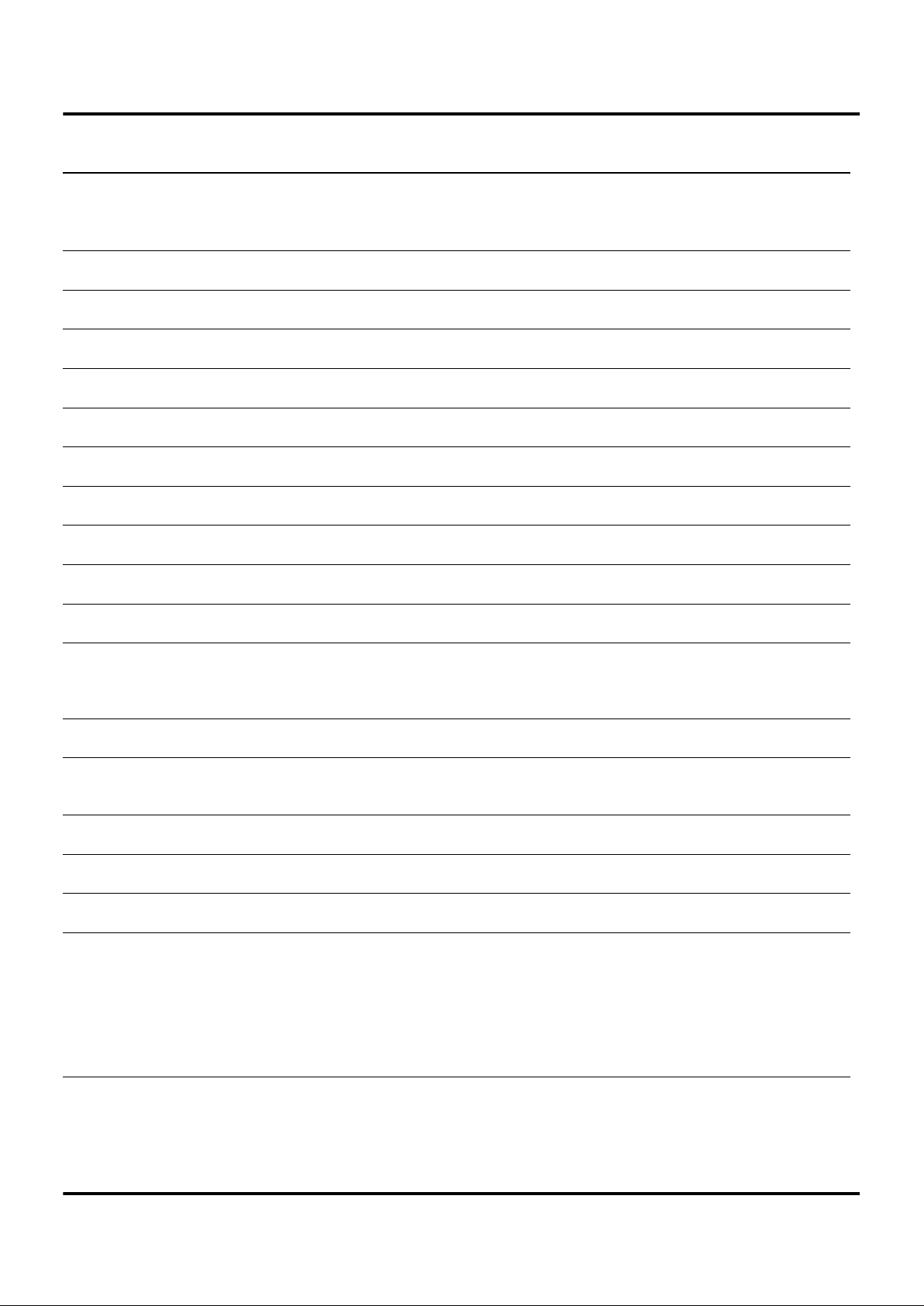
Port 0 (P07-P00). Port 0 is an two-bit, bidirectional,
CMOS-compatible port. These I/O lines are configured un-
der software control as an I/O port. The output drivers are
push-pull.
An optional 200 KOhm pull-up is available as a mask op-
tion on both Port 0 bits.
These pull-ups are disabled when configured (bit by
bit) as an output.
Figure 8. Port 0 Configuration
OEN
Out
In
PAD
200 KΩ
Mask
Option
Z86L70/71/75/C71
Zilog IR/Low-Voltage Microcontroller
DS97LVO0500 P R E L I M I N A R Y 1-15
1
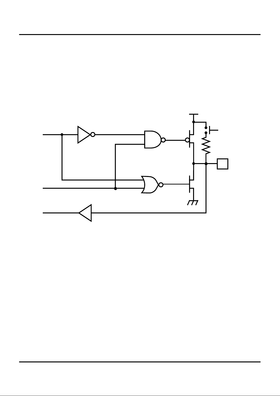
Port 2 (P27-P20). Port 2 is an 8-bit, bidirectional, CMOS-
compatible I/O port. These eight I/O lines can be indepen-
dently configured under software control as inputs or out-
puts. Port 2 is always available for I/O operation. A mask
option is available to connect eight 200 KOhms (±50%)
pull-up resistors on this port. Bits programmed as outputs
are globally programmed as either push-pull or open-
drain. The Z8 wakes up with the eight bits of Port 2 config-
ured as inputs with open-drain outputs.
Port 2 also has an 8-bit input OR and an AND gate which
can be used to wake up the part from STOP Mode (Figure
33). P20 can be programmed to access the edge selection
circuitry (Figure 9).
Figure 9. Port 2 Configuration
Open-Drain
OEN
Out
In
PAD
Port 2 (I/O)
Z86LXX
MCU
VCC
Mask
Option
200 KΩ
Z86L70/71/75/C71
IR/Low-Voltage Microcontroller Zilog
1-16 P R E L I M I N A R Y DS97LVO0500
PIN FUNCTIONS (Continued)
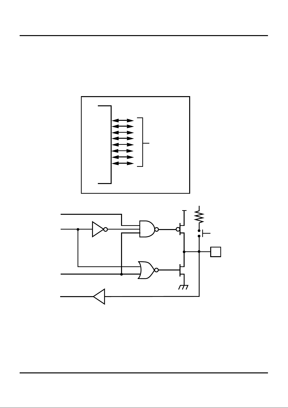
Port 3 (P36-P31). Port 3 is a 6-bit, CMOS-compatible
three fixed input and three fixed output port. Port 3 consists
of three fixed input (P33-P31) and three fixed output (P36-
P34), and can be configured under software control for In-
put/Output, Interrupt, and output from the counter/timers.
P31, P32, and P33 are standard CMOS inputs; outputs are
push-pull, except for P34, P35 which have floating drain
capability (controlled by P3M, D0).
Two on-board comparators process analog signals on P31
and P32 with reference to the voltage on P33. The analog
function is enabled by programming the Port 3 Mode Reg-
ister (bit 1). P31 and P32 are programmable as rising, fall-
ing, or both edge triggered interrupts (IRQ register bits 6
and 7). Pref1 and P33 are the comparator reference volt-
age inputs. Access to the Counter Timer edge detection
circuit is through P31 or P20 (see CTR1 description).
Port 3 provides the following control functions: three exter-
nal interrupt request signals (IRQ2-IRQ0).
Port 3 also provides output for each of the counter/timers
and the AND/OR Logic. Control is performed by program-
ming bits D5-D4 of CTRI, bit 0 of CTR0 and bit 0 of CTR2.
Table 2. Pin Assignments
Pin I/O C/T Comp. Int. Ext
P31 IN IN AN1 IRQ2
P32 IN AN2 IRQ0
P33 IN V
REF
IRQ1
P34 OUT T8 A01 DM
P35 OUT T16
P36 OUT T8/16
P20 I/O IN
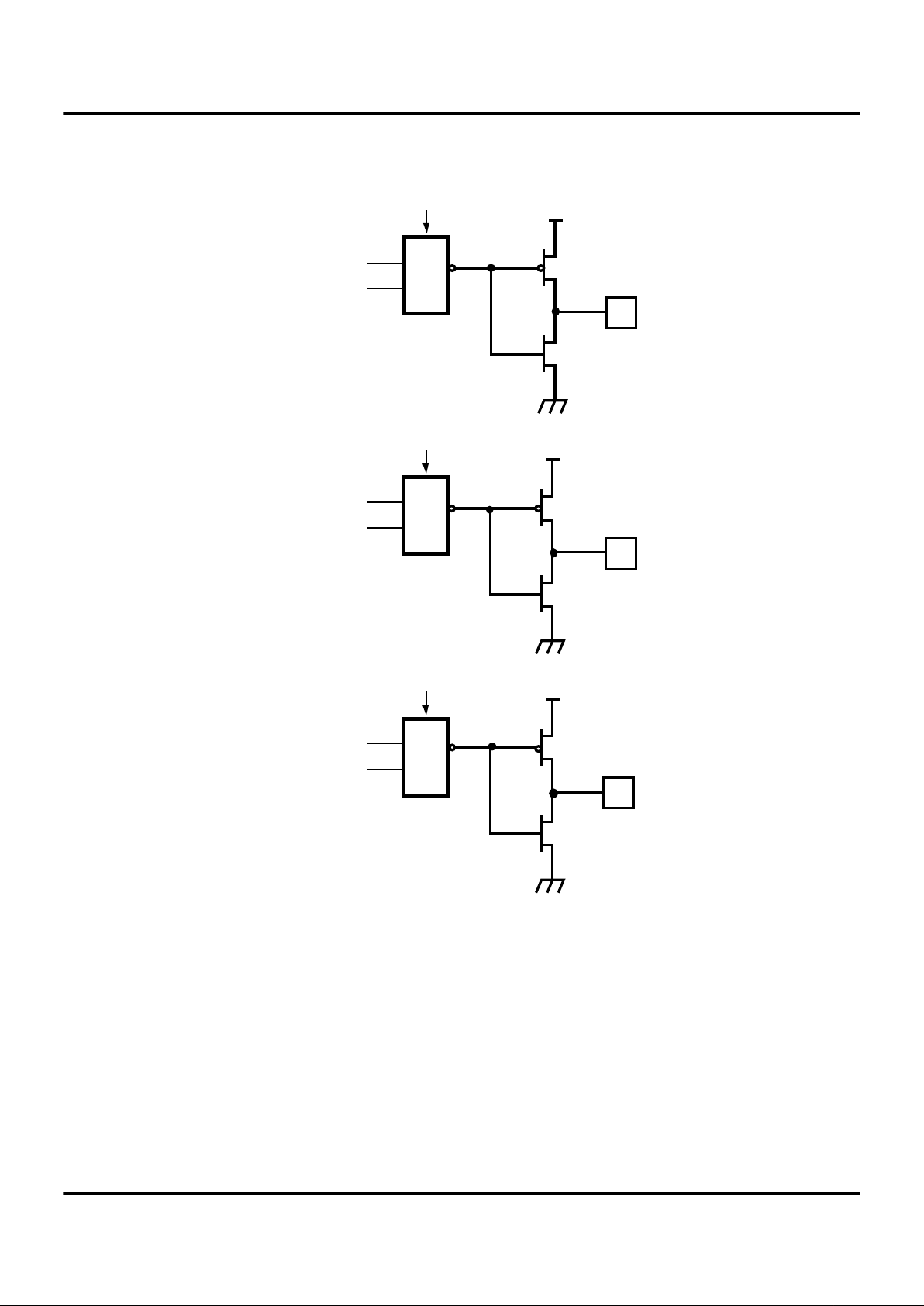
Figure 10. Port 3 Configuration
P34 OUT
P32
+
-
P33
0 = P34 Standard Output
1 = P34 Comparator Output
PCON
D0
P31
+
-
P33
P34
PAD
*
T8
P34 OUT
0 Normal Control
1 8-bit Timer output active
CTR0
D0
Counter/Timer
Reset condition.
*
Comp1
Comp2
Z86L70/71/75/C71
Zilog IR/Low-Voltage Microcontroller
DS97LVO0500 P R E L I M I N A R Y 1-17
1
Comparator Inputs. In Analog Mode, Port 3 (P31 and
P32) have a comparator front end. P33 serves as the ref-
erence for both comparators. In this mode, the P33 internal
data latch and its corresponding IRQ1 is diverted to the
SMR Sources (excluding P31, P32, and P33) as shown in
Figure 38. In digital mode, P33 is used as D3 of the Port 3
input register which then generates IRQ1 as shown in Fig-
ure 16.
Notes: Comparators are powered down by entering STOP
Mode. For P31-P33 to be used as a Stop-Mode Recovery
source, these inputs must be placed into digital mode.
Comparator Outputs. COMP1 may be programmed to be
outputted on P34 through the PCON register (Figure 15).
Power-On Reset. the typical reset output time is 5 ms.
The Z86L7X does not reset WDTMR, SMR, P2M, or P3M
registers on a Stop-Mode Recovery operation.
Figure 11. Port 3 Configuration
Port 3
(I/O or Handshake)
Z86L7X
MCU
Pref1
P31
P32
P33
P34
P35
P36
P37
Note:
P31, 32, 33 have a 200 KΩ
mask option
200 KΩ
Mask
Option
D1
R247 = P3M
P31 (AN1)
P32 (AN2)
P33 (REF2)
From Stop-Mode
Recovery Source of SMR
1 = Analog
0 = Digital
IRQ2, P31 Data Latch
IRQ0, P32 Data Latch
IRQ1, P33 Data Latch
DIG.
AN.
-
+
-
+
Pref
Comp1
Comp2
Z86L70/71/75/C71
IR/Low-Voltage Microcontroller Zilog
1-18 P R E L I M I N A R Y DS97LVO0500
PIN FUNCTIONS (Continued)
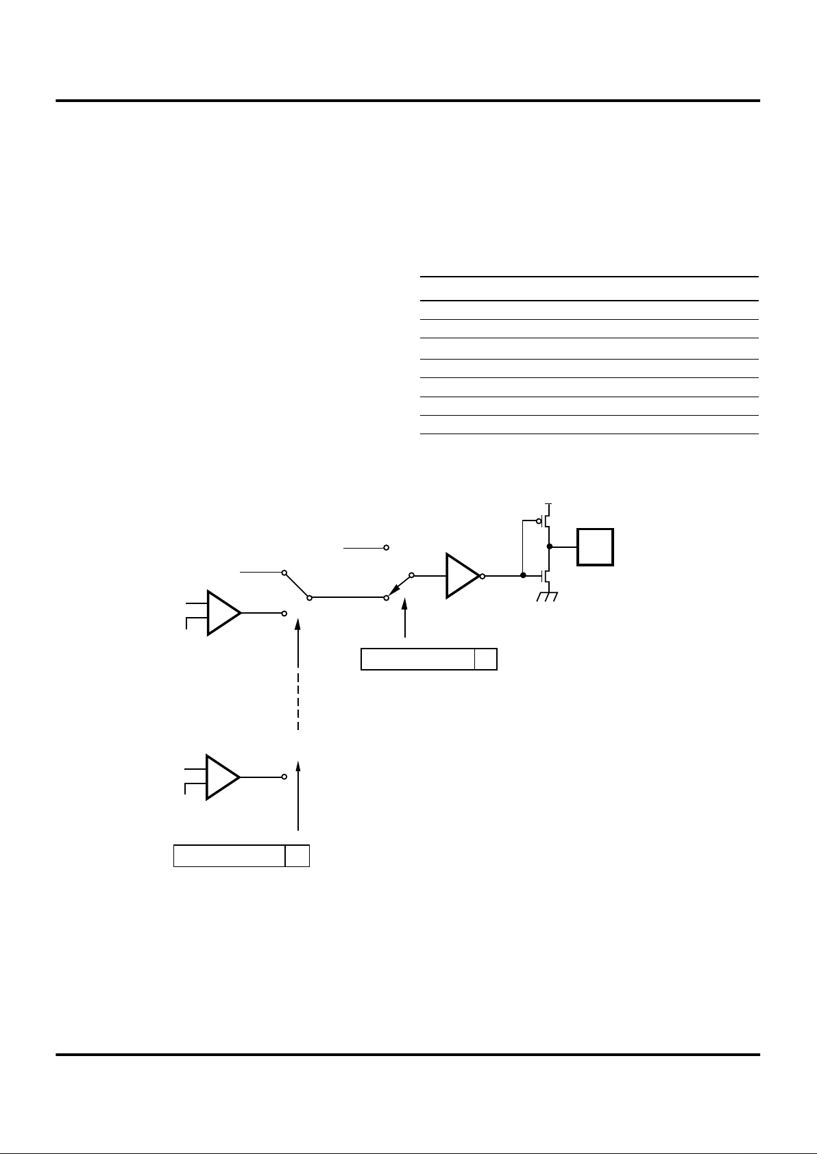
Figure 12. Port 3 Configuration
VDD
Out 34
T8_Out
CTR0, D0
Pad
Out 35
T16_Out
CTR2, D0
Out 36
T8/16_Out
CTR1, D6
MUX
MUX
MUX
P34
VDD
Pad
P35
VDD
Pad
P36
Z86L70/71/75/C71
Zilog IR/Low-Voltage Microcontroller
DS97LVO0500 P R E L I M I N A R Y 1-19
1
FUNCTIONAL DESCRIPTION
The Z8 incorporates special functions to enhance the Z8's
functionality in consumer and battery operated applica-
tions.
Reset. The device is reset in one of the following condi-
tions:
1. Power-On Reset
2. Watch-Dog Timer
3. Stop-Mode Recovery Source
4. Low Voltage Detection
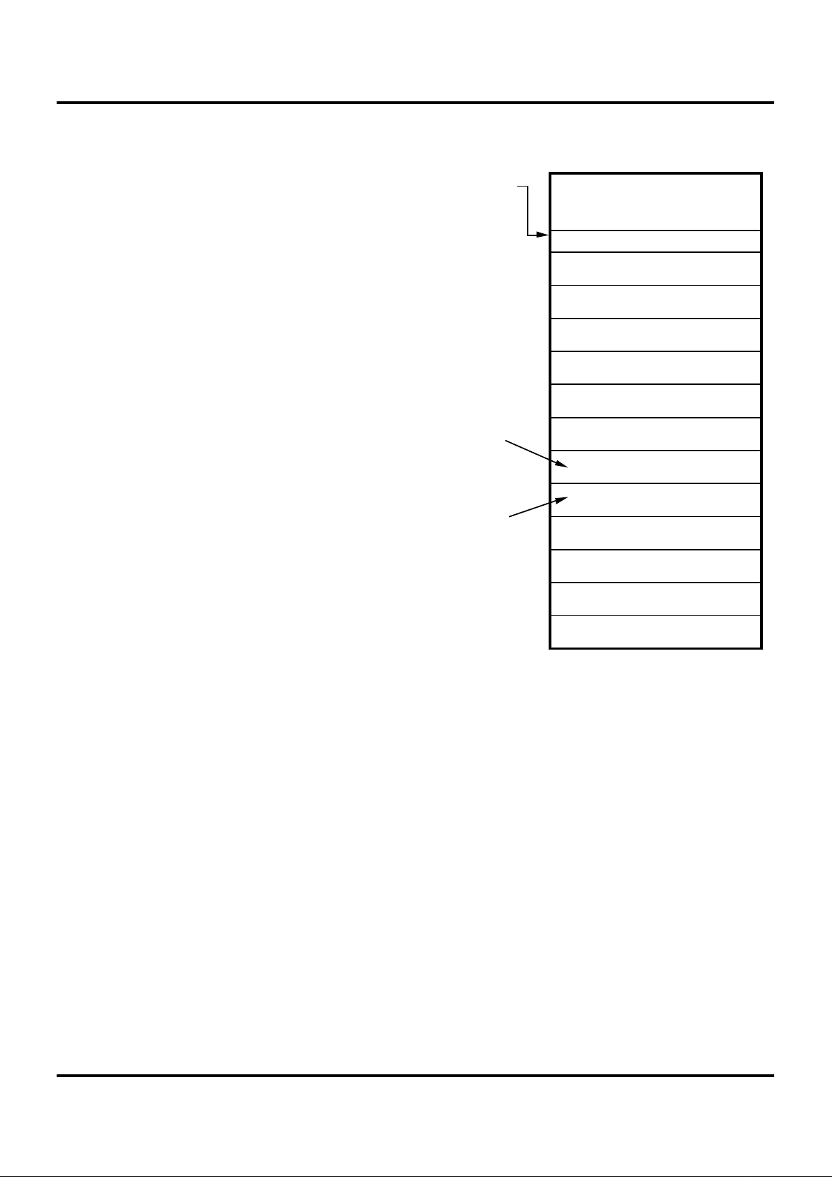
Program Memory. The Z86L7X addresses up to 2K, 4K,
8 KB of internal program memory, with the remainder be-
ing external memory (Figure 13). The first 12 bytes of pro-
gram memory are reserved for the interrupt vectors. These
locations contain five 16-bit vectors that correspond to the
five available interrupts. Addresses 12 to 2K, 4K, 8K (de-
pendent on version) consist of on-chip mask-programmed
ROM.
Figure 13. Program Memory Map
11
10
9
8
7
6
5
4
3
2
1
0
Location of
First Byte of
Instruction
Executed
After RESET
Interrupt
Vector
(Lower Byte)
Interrupt
Vector
(Upper Byte)
Reserved
IRQ4
IRQ4
IRQ3
IRQ3
IRQ2
IRQ2
IRQ1
IRQ1
IRQ0
IRQ0
Reserved
On-Chip
ROM
Reset Start Address
12
 Loading...