


Uniand Bipolar Hall IC Switches for |
TLE 4905 L; TLE 4935 L; |
|
Magnetic Field Applications |
TLE 4935-2 L; TLE 4945 L; |
|
|
|
TLE 4945-2L |
|
|
Bipolar IC |
Features |
|
|
• Temperature compensated magnetic performance |
|
|
• Digital output signal |
|
|
• For unipolar and alternating magnetic fields |
|
|
• Large temperature range |
|
|
• Protection against reversed polarity |
|
|
• Output protection against electrical disturbances |
|
|
|
|
P-SSO-3-2 |
Type |
Ordering Code |
Package |
TLE 4905 L |
Q67006-A9120 |
P-SSO-3-2 |
TLE 4935 L |
Q67006-A9112 |
P-SSO-3-2 |
TLE 4935-2 L |
Q67006-A9143 |
P-SSO-3-2 |
TLE 4945 L |
Q67006-A9163 |
P-SSO-3-2 |
TLE 4945-2L |
on request |
P-SSO-3-2 |
TLE 4905/35/35-2/45 L (Unipolar/Bipolar Magnetic Field Switches) have been designed specifically for automotive and industrial applications. Reverse polarity protection is included on-chip as is output protection against negative voltage transients.
Typical applications are position/proximity indicators, brushless DC motor commutation, rotational indexing etc.
Semiconductor Group |
1 |
1997-09-01 |
TLE 4905 L; TLE 4935 L;
TLE 4935-2 L; TLE 4945 L; TLE 4945-2L
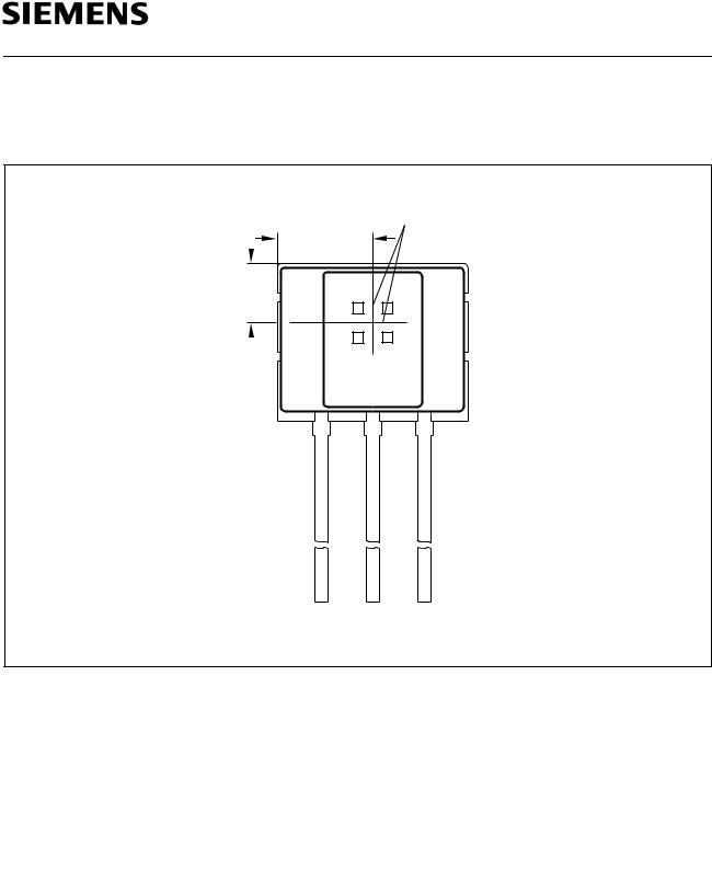
Pin Configuration
(view on branded side of component)
Center of sensitive area
2.08±0.15
1.35 ±0.15
1 |
2 |
3 |
VS GND Q
AEP01364
Figure 1
Pin Definitions and Functions
Pin No. |
Symbol |
Function |
|
|
|
1 |
VS |
Supply voltage |
2 |
GND |
Ground |
|
|
|
3 |
Q |
Output |
|
|
|
Semiconductor Group |
2 |
1997-09-01 |
TLE 4905 L; TLE 4935 L;
TLE 4935-2 L; TLE 4945 L; TLE 4945-2L
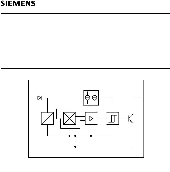
Circuit Description
The circuit includes Hall generator, amplifier and Schmitt-Trigger on one chip. The internal reference provides the supply voltage for the components. A magnetic field perpendicular to the chip surface induces a voltage at the hall probe. This voltage is amplified and switches a Schmitt-trigger with open-collector output. A protection diode against reverse power supply is integrated. The output is protected against electrical disturbances.
|
Threshold |
|
|
|
Generator |
|
|
V |
1 |
3 |
Q |
S |
Hall- |
|
|
|
|
|
|
|
Generator |
|
|
|
VS |
|
|
|
VRef |
|
|
|
Amplifier |
Schmitt- |
|
|
|
Trigger |
|
|
|
Output |
|
|
2 |
Stage |
|
|
|
|
|
|
GND |
AEB01243 |
|
Figure 2
Block Diagram
Semiconductor Group |
3 |
1997-09-01 |

TLE 4905 L; TLE 4935 L;
TLE 4935-2 L; TLE 4945 L; TLE 4945-2L
Functional Description Unipolar Type TLE 4905 (figure 3 and 4)
When a positive magnetic field is applied in the indicated direction (figure 3) and the turn-on magnetic induction BOP is exceeded, the output of the Hall-effect IC will conduct (Operate Point). When the current is reduced, the output of the IC turns off (Release Point; figure 4).
+
Branded Side
Ι
S
N  VQ
VQ
+ -
VS AES01231
Figure 3
Sensor/Magnetic-Field Configuration
B |
|
BOP |
|
BRP |
Induction |
0 |
t |
|
|
VQ |
|
VQH |
|
Output Voltage
VQL
t
AED01420
Figure 4
Switching Characteristics Unipolar Type
Semiconductor Group |
4 |
1997-09-01 |
TLE 4905 L; TLE 4935 L;
TLE 4935-2 L; TLE 4945 L; TLE 4945-2L
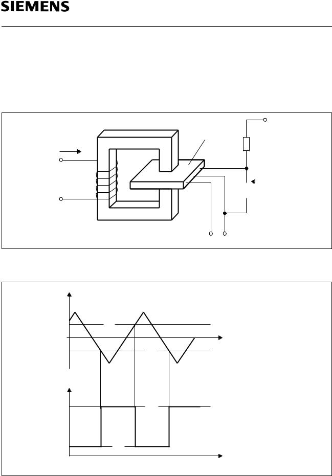
Functional Description Bipolar Type TLE 4935/35-2/45 (figure 5 and 6)
When a positive magnetic field is applied in the indicated direction (figure 5) and the turn-on magnetic induction BOP is exceeded, the output of the Hall-effect IC will conduct (Operate Point). When a reverse magnetic field is generated, the output of the IC turns off (Release Point; figure 6).
+
Branded Side
Ι
S
N  VQ
VQ
+ -
VS AES01231
Figure 5
Sensor/Magnetic-Field Configuration
|
B |
|
BOP |
0 |
Induction |
|
t |
|
BRP |
|
VQ |
|
VQH |
Output Voltage
VQL
t
AED01421
Figure 6
Switching Characteristics Bipolar Type
Semiconductor Group |
5 |
1997-09-01 |
 Loading...