


5-V Low-Drop Fixed Voltage Regulator |
TLE 4270 |
Features |
|
|
|
|
|
||
• |
Output voltage tolerance ≤ ± 2 % |
|
|
||||
• Low-drop voltage |
|
|
|
||||
• |
Integrated overtemperature protection |
|
|||||
• |
Reverse polarity protection |
|
|
||||
• Input voltage up to 42 V |
|
|
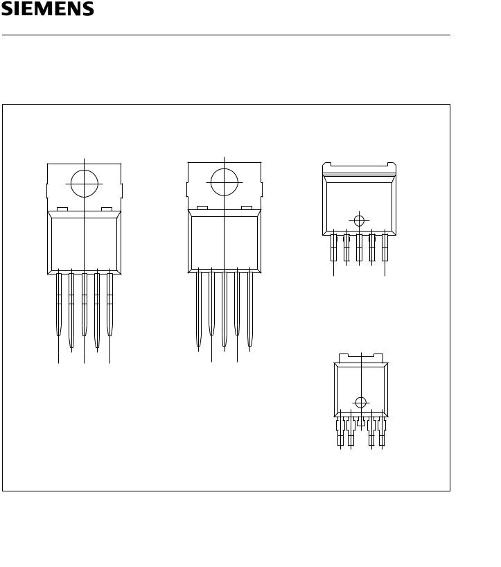
P-TO220-5-11 |
||||
• Overvoltage protection up to 65 V (≤ 400 ms) |
(P-TO220-5-1) |
||||||
• Short-circuit proof |
|
|
|
||||
• Suitable for use in automotive electronics |
|
||||||
• |
Wide temperature range |
|
|
|
|||
• |
Adjustable reset time |
|
|
|
|||
• |
ESD protection > 4000 V |
|
|
|
|||
Type |
|
Ordering Code |
Package |
P-TO220-5-12 |
|||
TLE 4270 |
|
Q67000-A9209-A903 |
P-TO220-5-11 |
||||
|
(P-TO220-5-2) |
||||||
TLE 4270 |
S |
Q67000-A9243-A904 |
P-TO220-5-12 |
|
|||
TLE 4270 |
G |
Q67006-A9201-A901 |
P-TO263-5-1 |
|
|||
▼ TLE 4270 |
|
Q67000-A9209-A801 |
P-TO220-5-1 |
|
|||
▼ TLE 4270 |
S |
Q67000-A9243-A802 |
P-TO220-5-2 |
|
|||
▼ TLE 4270 |
G |
Q67006-A9201-A802 |
P-TO220-5-8 |
P-TO263-5-1 |
|||
● TLE 4270 D |
Q67006-A9360 |
P-TO252-5-1 |
|||||
(P-TO220-5-8) |
|||||||
|
|
|
|
|
|
||
▼ Not for new design |
● New type |
|
|||||
Functional Description
This device is a 5-V low-drop fixed-voltage regulator. The maximum input voltage is 42 V (65 V, ≤ 400 ms). Up to an input voltage of 26 V and for an output current
up to 550 mA it regulates the output voltage within a 2 % accuracy. The short circuit protection limits the
output current of more than 650 mA. The device incorporates overvoltage protection and temperature protection that disables the circuit at unpermissibly high temperatures.
Semiconductor Group |
1 |
1998-11-01 |
TLE 4270
Pin Configuration
(top view)
P-TO220-5-11 |
P-TO220-5-12 |
P-TO263-5-1 |
(P-TO220-5-1) |
(P-TO220-5-2) |
(P-TO220-5-8) |
1 |
5 |
RO D
ΙGND Q
AEP01923
1 |
5 |
Ι GND |
Q |
RO |
D |
AEP02172
1 |
5 |
RO  D
D
ΙGND Q
AEP01922
P-TO252-5-1 (D-PAK)
|
GND |
1 |
5 |
Ι RO D Q
AEP02580
Figure 1
Pin Definitions and Functions
Pin |
Symbol |
Function |
|
|
|
|
|
||
1 |
I |
Input; block to ground directly on the IC with ceramic capacitor |
||
|
|
|
||
2 |
RO |
Reset Output; the open collector output is connected to the 5 V output |
||
|
|
via an integrated resistor of 30 kΩ. |
|
|
|
|
|
|
|
3 |
GND |
Ground; internally connected to heatsink. |
|
|
|
|
|
||
4 |
D |
Reset Delay; connect a capacitor to ground for delay time adjustment. |
||
|
|
|
||
5 |
Q |
5-V Output; block to ground with 22 µF capacitor, ESR < 3 Ω. |
||
|
|
|
|
|
Semiconductor Group |
2 |
1998-11-01 |
||

TLE 4270
Application Description
The IC regulates an input voltage in the range of 5.5 V < VI < 36 V to VQnom = 5.0 V. Up to 26 V it produces a regulated output current of more than 550 mA. Above 26 V the
save-operating-area protection allows operation up to 36 V with a regulated output current of more than 300 mA. Overvoltage protection limits operation at 42 V. The overvoltage protection hysteresis restores operation if the input voltage has dropped below 36 V. A reset signal is generated for an output voltage of VQ < 4.5 V. The delay for power-on reset can be set externally with a capacitor.
Design Notes for External Components
An input capacitor CI is necessary for compensation of line influences. The resonant circuit consisting of lead inductance and input capacitance can be damped by a resistor of approx. 1 Ω in series with CI. An output capacitor CQ is necessary for the stability of
the regulating circuit. Stability is guaranteed at values of CQ ≥ 22 µF and an ESR of
< 3 Ω.
Circuit Description
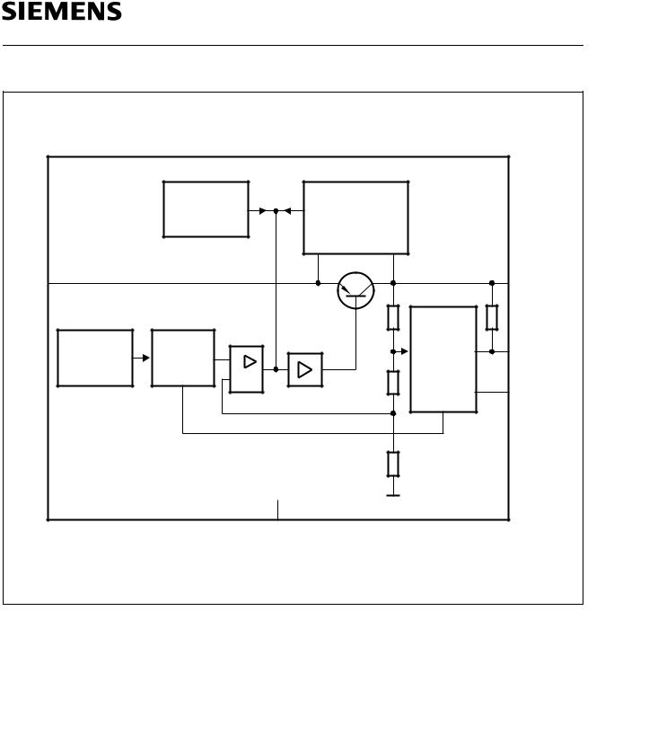
The control amplifier compares a reference voltage, which is kept highly accurate by resistance adjustment, to a voltage that is proportional to the output voltage and drives the base of a series transistor via a buffer. Saturation control as a function of the load current prevents any over-saturation of the power element.
If the output voltage decreases below 4.5 V, an external capacitor CD on pin 4 (D) will be discharged by the reset generator. If the voltage on this capacitor drops below VDRL, a reset signal is generated on pin 2 (RO), i.e. reset output is set low. If the output voltage rises above 4.5 V, CD will be charged with constant current. After the power-on-reset time the voltage on the capacitor reaches VDU and the reset output will be set high again. The value of the power-on-reset time can be set within a wide range depending of the capacitance of CD.
The IC also incorporates a number of internal circuits for protection against:
•Overload
•Overvoltage
•Overtemperature
•Reverse polarity
Semiconductor Group |
3 |
1998-11-01 |
TLE 4270
|
|
Temperature |
Saturation |
|
|
|
|
Control and |
|
||
|
|
Sensor |
|
|
|
|
|
|
Protection |
|
|
|
|
|
|
|
|
|
|
|
|
Circuit |
|
Input |
1 |
|
|
5 |
Output |
|
|
|
Control |
|
|
|
|
|
Amplifier |
2 |
Reset |
|
|
Bandgap |
Buffer |
||
|
Adjustment |
+ |
Reset |
Output |
|
|
Reference |
||||
|
|
- |
Generator |
|
|
|
|
|
4 |
Reset |
|
|
|
|
|
|
Delay |
|
|
|
3 |
|
|
|
|
|
GND |
|
AEB01924 |
Figure 2
Block Diagram
Semiconductor Group |
4 |
1998-11-01 |

TLE 4270
Absolute Maximum Ratings
Tj = – 40 to 150 °C
Parameter |
Symbol |
|
Limit Values |
Unit |
Notes |
|
|
|
|
|
|
|
|
|
|
min. |
|
max. |
|
|
|
|
|
|
|
|
|
Input |
|
|
|
|
|
|
|
|
|
|
|
|
|
Voltage |
VI |
– 42 |
|
42 |
V |
t ≤ 400 ms |
Voltage |
VI |
|
|
65 |
V |
|
Current |
II |
|
|
|
|
internally limited |
|
|
|
|
|
|
|
Reset Output |
|
|
|
|
|
|
|
|
|
|
|
|
|
Voltage |
VR |
– 0.3 |
|
7 |
V |
|
Current |
IR |
|
|
|
|
Internally limited |
Reset Delay |
|
|
|
|
|
|
|
|
|
|
|
|
|
Voltage |
VD |
– 0.3 |
|
7 |
V |
|
Current |
ID |
|
|
|
|
Internally limited |
Output |
|
|
|
|
|
|
|
|
|
|
|
|
|
Voltage |
VQ |
– 1.0 |
|
16 |
V |
|
Current |
IQ |
|
|
|
|
Internally limited |
Ground |
|
|
|
|
|
|
|
|
|
|
|
|
|
Current |
IGND |
– 0.5 |
|
– |
A |
– |
Temperatures |
|
|
|
|
|
|
|
|
|
|
|
|
|
Junction temperature |
Tj |
|
|
150 |
°C |
– |
Storage temperature |
Tstg |
– 50 |
|
150 |
°C |
|
Optimum reliability and life time are guaranteed if the junction temperature does not exceed 125 °C in operating mode. Operation at up to the maximum junction temperature of 150 °C is possible in principle. Note, however, that operation at the maximum permitted ratings could affect the reliability of the device.
Semiconductor Group |
5 |
1998-11-01 |

TLE 4270
Operating Range
Parameter |
|
Symbol |
|
Limit Values |
Unit |
Notes |
|
|
||||
|
|
|
|
|
|
|
|
|
|
|
|
|
|
|
|
|
min. |
max. |
|
|
|
|
|
||
|
|
|
|
|
|
|
|
|
|
|
|
|
Input voltage |
|
VI |
6 |
|
42 |
V |
– |
|
||||
|
|
|
|
|
|
|
|
|
|
|
|
|
Junction temperature |
|
Tj |
– 40 |
150 |
°C |
– |
|
|||||
|
|
|
|
|
|
|
|
|
|
|
|
|
Thermal Resistance |
|
|
|
|
|
|
|
|
|
|
|
|
|
|
|
|
|
|
|
|
|
|
|
|
|
Junction ambient |
|
Rthja |
– |
65 |
K/W |
TO263, TO2521) |
|
|
||||
|
|
|
|
|
|
70 |
K/W |
|
||||
Junction case |
|
Rthjc |
– |
3 |
K/W |
t < 1 ms |
|
|||||
|
|
Zthjc |
|
|
2 |
K/W |
(TO-220/263 |
|
||||
|
|
|
|
|
|
|
|
|
|
Packages) |
|
|
|
|
|
|
|
|
|
|
|
|
|
|
|
1) Soldered in, min. footprint |
|
|
|
|
|
|
|
|
|
|
|
|
Characteristics |
|
|
|
|
|
|
|
|
|
|
|
|
VI = 13.5 V; – 40 °C ≤ Tj = ≤ 125 °C (unless otherwise specified) |
|
|
|
|||||||||
|
|
|
|
|
|
|
|
|
|
|
||
Parameter |
Symbol |
|
Limit Values |
Unit |
|
Test Condition |
|
|||||
|
|
|
|
|
|
|
|
|
|
|
|
|
|
|
|
min. |
|
typ. |
|
max. |
|
|
|
|
|
|
|
|
|
|
|
|
|
|
|
|
|
|
Output voltage |
VQ |
|
4.90 |
|
5.00 |
|
5.10 |
V |
|
5 mA ≤ IQ ≤ 550 mA; |
|
|
|
|
|
|
|
|
|
|
|
|
6 V ≤ VI ≤ 26 V |
|
|
|
|
|
|
|
|
|
|
|
|
|
|
|
Output voltage |
VQ |
|
4.90 |
|
5.00 |
|
5.10 |
V |
|
26 V ≤ VI ≤ 36 V; |
|
|
|
|
|
|
|
|
|
|
|
|
IQ ≤ 300 mA |
|
|
|
|
|
|
|
|
|
|
|
|
|
||
|
|
|
|
|
|
|
|
|
|
|
|
|
Output current |
IQmax |
|
650 |
|
850 |
|
– |
mA |
VQ = 0 V |
|
||
limiting |
|
|
|
|
|
|
|
|
|
|
|
|
|
|
|
|
|
|
|
|
|
|
|
|
|
Current |
Iq |
|
– |
|
1 |
|
1.5 |
mA |
IQ = 5 mA |
|
||
consumption |
|
|
|
|
|
|
|
|
|
|
|
|
Iq = II − IQ |
|
|
|
|
|
|
|
|
|
|
|
|
|
|
|
|
|
|
|
|
|
|
|
|
|
Current |
Iq |
|
– |
|
55 |
|
75 |
mA |
IQ = 550 mA |
|
||
consumption |
|
|
|
|
|
|
|
|
|
|
|
|
Iq = II – IQ |
|
|
|
|
|
|
|
|
|
|
|
|
|
|
|
|
|
|
|
|
|
|
|
|
|
Current |
Iq |
|
– |
|
70 |
|
90 |
mA |
IQ = 550 mA; VI = 5 V |
|
||
consumption |
|
|
|
|
|
|
|
|
|
|
|
|
Iq = II – IQ |
|
|
|
|
|
|
|
|
|
|
|
|
|
|
|
|
|
|
|
|
|
|
|
|
|
Drop voltage |
V |
|
– |
|
350 |
|
700 |
mV |
|
I = 550 mA1) |
|
|
|
dr |
|
|
|
|
|
|
|
|
Q |
|
|
Semiconductor Group |
|
|
|
6 |
|
|
|
|
1998-11-01 |
|
|
|
 Loading...