


Siemens TLE4276V85, TLE4276V, TLE4276SV50, TLE4276SV85, TLE4276SV10 Datasheet
...
Low-Drop Voltage Regulator |
TLE 4276 |
Features |
|
|
|
||
• |
Output voltage tolerance ≤ ± 4% |
|
|
||
• Low-drop voltage |
|
|
|||
• |
Inhibit input |
|
|
|
|
• Very low current consumption |
|
|
|||
• |
Short-circuit-proof |
|
|
||
• |
Reverse polarity proof |
|
|
||
• Suitable for use in automotive electronics |
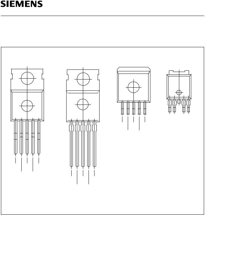
P-TO220-5-3 |
||||
Type |
Ordering Code |
Package |
|
||
TLE 4276 V50 |
Q67000-A9262 |
P-TO220-5-3 |
|
||
TLE 4276 V85 |
Q67000-A9263 |
P-TO220-5-3 |
|
||
TLE 4276 V10 |
Q67000-A9264 |
P-TO220-5-3 |
|
||
TLE 4276 G V50 |
Q67006-A9266 |
P-TO220-5-122 |
|
||
TLE 4276 G V85 |
Q67006-A9268 |
P-TO220-5-122 |
P-TO220-5-43 |
||
TLE 4276 G V10 |
Q67006-A9270 |
P-TO220-5-122 |
|||
|
|||||
TLE 4276 S V50 |
Q67000-A9267 |
P-TO220-5-43 |
|
||
TLE 4276 S V85 |
Q67000-A9269 |
P-TO220-5-43 |
|
||
TLE 4276 S V10 |
Q67000-A9271 |
P-TO220-5-43 |
|
||
TLE 4276 V |
Q67000-A9265 |
P-TO220-5-3 |
|
||
TLE 4276 SV |
Q67000-A9273 |
P-TO220-5-43 |
|
||
TLE 4276 GV |
Q67006-A9272 |
P-TO220-5-122 |
|
||
▼ TLE 4276 D V50 |
Q67006-A9358 |
P-TO252-5-1 |
P-TO220-5-122 |
||
▼ TLE 4276 DV |
Q67006-A9361 |
P-TO252-5-1 |
|
||
|
SMD = Surface Mounted Device |
|
|
||
▼ New type |
|
|
|
||
P-TO252-5-1 (D-PAK)
Semiconductor Group |
1 |
1998-11-01 |

TLE 4276
Functional Description
The TLE 4276 is a low-drop voltage regulator in a TO220 package. The IC regulates an
input voltage up to 40 V to VQrated = 5.0 V (V50), 8.5 V (V85), 10 V (V10) and adjustable voltage (V). The maximum output current is 400 mA. The IC can be switched off via the
inhibit input, which causes the current consumption to drop below 10 µA. The IC is short- circuit-proof and incorporates temperature protection that disables it at over-tempera- ture.
Dimensioning Information on External Components
The input capacitor CI is necessary for compensating line influences. Using a resistor of approx. 1 Ω in series with CI, the oscillating of input inductivity and input capacitance can be damped. The output capacitor CQ is necessary for the stability of the regulation circuit. Stability is guaranteed at values CQ ≥ 22 µF and an ESR of ≤ 3 Ω within the operating temperature range.
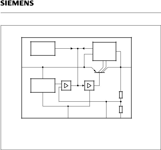
Circuit Description
The control amplifier compares a reference voltage to a voltage that is proportional to the output voltage and drives the base of the series transistor via a buffer. Saturation control as a function of the load current prevents any oversaturation of the power element. The IC also incorporates a number of internal circuits for protection against:
•Overload
•Overtemperature
•Reverse polarity
Semiconductor Group |
2 |
1998-11-01 |
TLE 4276
Pin Configuration
(top view)
P-TO220-5-3
1 |
5 |
P-TO220-5-43 P-TO220-5-122
1 |
5 |
1 |
5 |
Ι GND Q
INH N.C.
AEP02043
P-TO252-5-1
|
GND |
1 |
5 |
Ι Q INH N.C.
(VA)
AEP02560
Ι GND |
Q |
INH N.C. |
Ι GND Q |
(VA) |
AEP02041 |
INH N.C. |
|
|
|
(VA) |
|
AEP02042 |
Figure 1
Pin Definitions and Functions
Pin No. |
Symbol |
Function |
|
|
|
|
|
1 |
I |
Input; block to ground directly at the IC with a ceramic capacitor. |
|
|
|
|
|
2 |
INH |
Inhibit; low-active input |
|
|
|
|
|
3 |
GND |
Ground |
|
|
|
|
|
4 |
N.C. |
Not connected for V50, V85, V10 |
|
|
VA |
Voltage Adjust Input; only for adjustable output from external |
|
|
|
voltage divider. |
|
|
|
|
|
5 |
Q |
Output; block to ground with a ≥ 22 F capacitor. |
|
|
|
|
|
Semiconductor Group |
3 |
1998-11-01 |
|
TLE 4276
|
Temperature |
Saturation |
|
|
|
Sensor |
Control and |
|
|
|
|
Protection |
|
|
|
|
Circuit |
|
|
Ι |
1 |
|
6 |
Q |
|
Control |
|
|
|
|
Amplifier |
Buffer |
|
|
|
Bandgap |
|
|
|
|
Reference |
|
|
|
|
|
|
*) |
|
|
|
**) |
|
|
|
2 |
4 |
3 |
|
|
INH |
VA |
GND |
|
*) |
For fixed Voltage Regulator only |
|
**) |
For adjustable Voltage Regulator only |
AEB02044 |
Figure 2
Block Diagram
Semiconductor Group |
4 |
1998-11-01 |

TLE 4276
Absolute Maximum Ratings
Tj = – 40 to 150 °C
Parameter |
Symbol |
Limit Values |
Unit |
Test Condition |
|
|
|
|
|
|
|
|
|
|
|
|
|
min. |
max. |
|
|
|
|
|
|
|
|
|
|
|
|
Voltage Regulator |
|
|
|
|
|
|
|
Input |
|
|
|
|
|
|
|
|
|
|
|
|
|
|
|
Voltage |
VI |
– 42 |
45 |
V |
– |
|
|
Current |
II |
– |
– |
– |
Internally limited |
|
|
|
|
|
|
|
|
|
|
Inhibit |
|
|
|
|
|
|
|
|
|
|
|
|
|
|
|
Voltage |
VINH |
– 42 |
45 |
V |
– |
|
|
Voltage Adjust Input |
|
|
|
|
|
|
|
|
|
|
|
|
|
|
|
Voltage |
VVA |
– 0.3 |
10 |
V |
– |
|
|
Output |
|
|
|
|
|
|
|
|
|
|
|
|
|
|
|
Voltage |
VQ |
– 1.0 |
40 |
V |
– |
|
|
Current |
IQ |
– |
– |
– |
Internally limited |
|
|
|
|
|
|
|
|
|
|
Ground |
|
|
|
|
|
|
|
|
|
|
|
|
|
|
|
|
|
|
|
|
|
|
|
Current |
IGND |
– |
100 |
mA |
– |
|
|
Temperature |
|
|
|
|
|
|
|
|
|
|
|
|
|
|
|
Junction temperature |
Tj |
– |
150 |
°C |
– |
|
|
|
|
|
|
|
|
|
|
Storage temperature |
Tstg |
– 50 |
150 |
°C |
– |
|
|
|
|
|
|
|
|
|
|
Note: Maximum ratings are absolute ratings; exceeding any one of these values may cause irreversible damage to the integrated circuit.
Semiconductor Group |
5 |
1998-11-01 |
 Loading...