


Intelligent Sixfold Low-Side Switch
Features
●Double low-side switch, 2 x 0.5 A
●Quad low-side switch, 4 x 50 mA
●Power limitation
●Open-collector outputs
●Overtemperature shutdown
●Status monitoring
●Shorted-load protection
●Integrated clamp Z-Diodes
●Temperature range – 40 to 110 °C
TLE 4216 G
Bipolar IC
P-DSO-24-3
Type |
Ordering Code |
Package |
|
|
|
TLE 4216 G |
Q67000-A9108 |
P-DSO-24-3 (SMD) |
|
|
|
TLE 4216 G is an integrated, sixfold low-side power switch with power limiting of the 0.5 A outputs, shorted load protection of the 50 mA switches and Z-diodes on all switches from output to ground. TLE 4216 G is particularly suitable for automotive and industrial applications.
Semiconductor Group |
1 |
08.96 |
TLE 4216 G
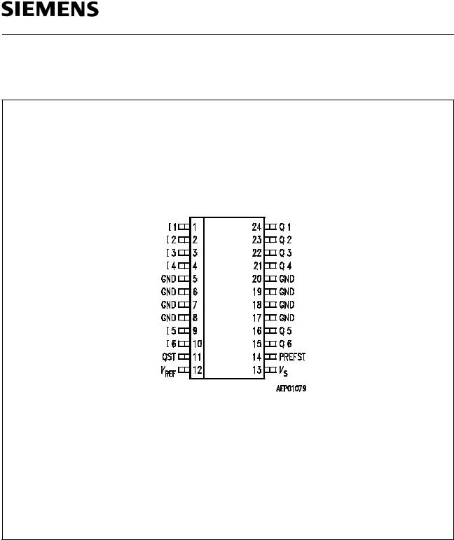
Pin Configuration
(top view)
TLE 4216 G
Semiconductor Group |
2 |

TLE 4216 G
Pin Definitions and Functions
TLE 4216 G |
Symbol |
Function |
|
|
|
Pin No. |
|
|
|
|
|
1, 2, 3, 4 |
I1, I2, I3, I4 |
Inputs of 50-mA switches 1, 2, 3, 4 |
|
|
|
5, 6, 7, 8 |
GND |
Ground, cooling |
|
|
|
9, 10 |
I5, I6 |
Inputs of 0.5 A switches 5, 6 |
|
|
|
11 |
QST |
Status analog output |
12 |
VREF |
Reference voltage; a higher reference voltage than |
|
|
the internal one can be applied from the exterior as |
|
|
a voltage reference for the status output (A/D |
|
|
converter). |
|
|
|
13 |
VS |
Supply voltage |
|
|
|
14 |
PREFST |
Preferred state (low = preferred state of all outputs |
|
|
regardless of inputs) |
|
|
|
15, 16 |
Q6, Q5 |
Outputs 6, 5 (0.5 A), open collector |
|
|
|
17, 18, 19, 20 |
GND |
Ground, cooling |
|
|
|
21, 22, 23, 24 |
Q4, Q3, |
Outputs 4, 3, 2, 1 (50 mA), open collector |
|
Q2, Q1 |
|
|
|
|
Semiconductor Group |
3 |

TLE 4216 G |
Block Diagram
Semiconductor Group |
4 |

TLE 4216 G
Circuit Description
Input Circuits
The control inputs and the preferred-state input consist of TTL-compatible Schmitt triggers with hysteresis. Driven by these stages the buffer amplifiers convert the logic signal necessary for driving the NPN power transistors.
Switching Stages
The output stages consist of NPN power transistors with open collectors. Each stage has its own protective circuit for limiting power dissipation and shorted-load current, which makes the outputs shorted-load protected to the supply voltage throughout the operating range. Integrated Z-diodes limit positive voltage spikes that occur when inductive loads are discharged.
Monitoring and Protective Functions
Each output is monitored in its activated status for overload. Furthermore, large parts of the circuitry are shutdown (control, output stages). The information from these malfunctions is ORed and applied to the status output. If several malfunctions appear simultaneously, the highest voltage level will dominate. The IC is also protected against thermal overload. If a chip temperature of typically 160 °C is reached, overtemperature is signalled on the status output. If the temperature continues to increase, all outputs are turned off at 170 °C.
If the minimum supply voltage for functioning is not maintained, the output stages become inactive. At a supply voltage of 2 to 4 V, the outputs are switched to a preferred state regardless of the level on pin PREFST. If the preferred state is to be maintained beyond this range, pin PREFST must be switched to low potential. Above a supply voltage of typical 3 V (max. 4 V) the preferred state is controlled by pin PREFST. From 4 to 5.2 V the logic operation of the outputs is guaranteed, but the status output cannot be evaluated. At a supply voltage of 5.2 to 30 V the full function is guaranteed.
Semiconductor Group |
5 |
 Loading...