


TLE4274V10
Siemens TLE4274V10, TLE4274GV85, TLE4274GV50, TLE4274DV50, TLE4274GV10 Datasheet
...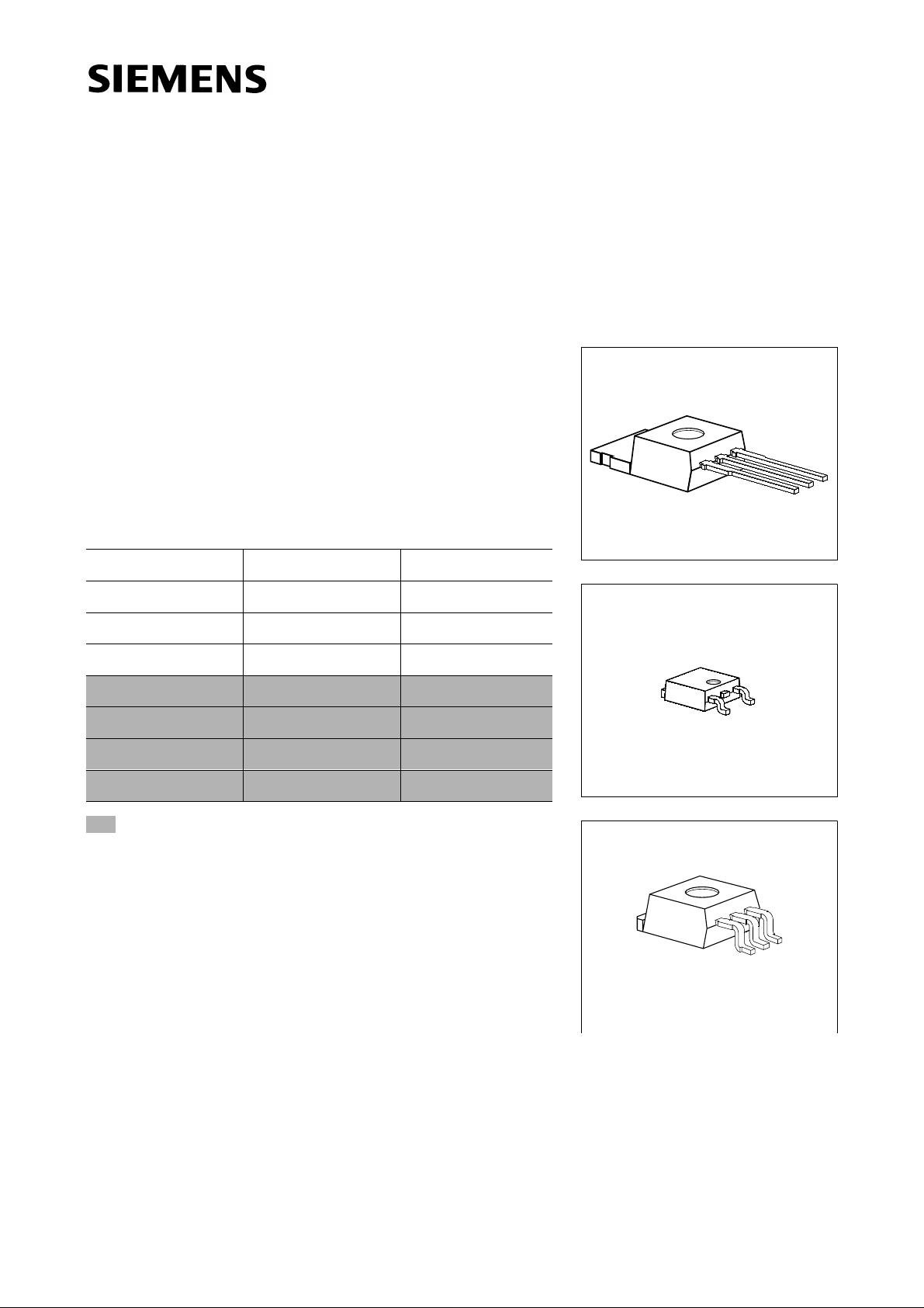
P-TO220-3-1
P-TO252-3-1
P-TO263-3-1
Low-Drop Voltage Regulator TLE 4274
Semiconductor Group 1 1998-11-01
Features
• Output voltage tolerance ≤ ± 4 %
• Low-drop voltage
• Very low current consumption
• Short-circuit proof
• Reverse polarity proof
• Suitable for use in automotive electronics
SMD = Surface Mounted Device
Functional Description
The TLE 4274 is a low-drop voltage regulator in a
TO220 package. The IC regulate s an inpu t vol tage up
to 40 V to
V
Qrated
= 5.0 V (V50), 8.5 V (V85) and 10 V
(V10). The maximum output current is 400 mA. The IC
is short-circuit proof and incorporates temperature
protection that disables the IC at over temperature.
Type Ordering Code Package
TLE 4274 V10 Q67000-A9258 P-TO220-3-1
TLE 4274 V85 Q67000-A9257 P-TO220-3-1
TLE 4274 V50 Q67000-A9256 P-TO220-3-1
TLE 4274 D V50 Q67006-A9331 P-TO252-3-1
TLE 4274 G V10 Q67006-A9261 P-TO263-3-1
TLE 4274 G V50 Q67006-A9259 P-TO263-3-1
TLE 4274 G V85 Q67006-A9260 P-TO263-3-1
Dimensioning Information on External Components
The input capacitor
C
I
is necessary for compensating line influences. Using a resistor of
approx. 1
Ω
in series with
C
I
, the oscillating of input inductivity and input capacitance can
be damped. The output capacitor
C
Q
is necessary for the stability of the regulation circuit.
Stability is guaranteed at values
C
Q
≥ 22 µF and an ESR of ≤ 3 Ω within the operating
temperature range.
TLE 4274
Semiconductor Group 2 1998-11-01
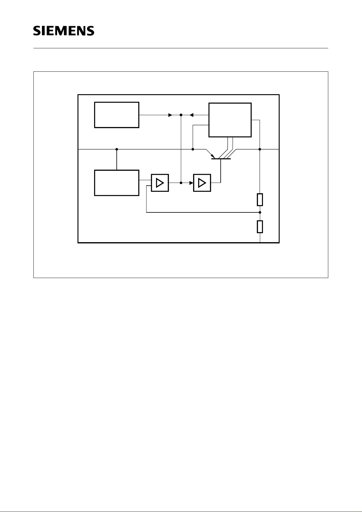
Circuit Description
The control amplifier compares a reference voltage to a voltage that is proportional to the
output voltage and drives the base of the series transistor via a buffer. Saturation control
as a function of the load current prevents any oversaturation of the power element. The
IC also incorporates a number of internal circuits for protection against:
• Overload
• Overtemperature
• Reverse polarity
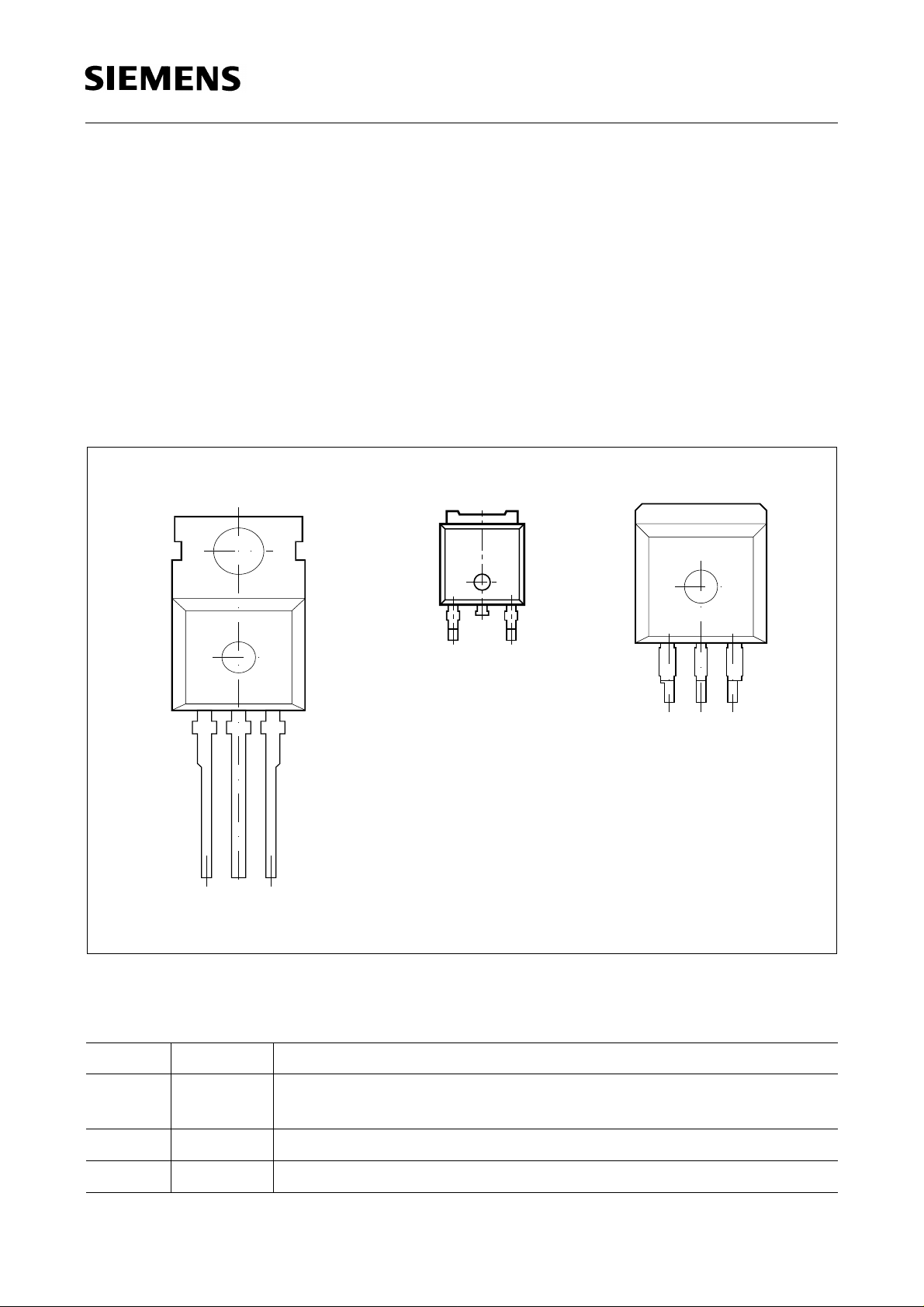
Pin Configuration (top view)
Figure 1
Pin Definitions and Functions
Pin No. Symbol Function
1 I Input; block to ground directly at the IC with a ceramic
capacitor.
2GNDGround
3Q Output; block to ground with a ≥ 22 µF capacitor.
GND
AEP01957
Ι
Q
P-TO220-3-1
P-TO263-3-1
GND
Ι
Q
AEP02281
P-TO252-3-1
AEP02512
Ι
GND
Q
TLE 4274
Semiconductor Group 3 1998-11-01
Figure 2
Block Diagram
Ι
1
AEB01959
GND
2
Q
3
Bandgap
Reference
Control
Amplifier
Sensor
Temperature
Buffer
Saturation
Control and
Protection
Circuit

TLE 4274
Semiconductor Group 4 1998-11-01
Note: Maximum ratin gs are absolute ratings; exceeding any one of these values may
cause irreversible damage to the integrated circuit.
Absolute Maximum Ratings
T
j
= – 40 to 150 °C
Parameter Symbol Limit Values Unit Test Condition
min. max.
Voltage Regulator
Input
Voltage
V
I
–42 45
V
–
Current
I
I
––
–
Internally limited
Output
Voltage
V
Q
–1.0 40 V –
Current
I
Q
– – – Internally limited
Ground
Current
I
GND
–100mA–
Temperature
Junction temperature
T
j
–150°C–
Storage temperature
T
stg
–50 150 °C–
Operating Range
Parameter Symbol Limit Values Unit Remarks
min. max.
Input voltage
V
I
5.5
9.0/10.5
40
40/40
V
V50
V85/V10
Junction temperature
T
j
–40 150 °C–
Thermal Resistance
Junction ambient
R
thja
–65K/WTO220
Junction ambient
R
thja
–70K/WTO252
1)
, TO263
1)
Soldered in, min. footprint
Junction case R
thjc
–4K/W–
 Loading...