


5-V Low-Drop Voltage Regulator |
TLE 4263 |
Features
●Output voltage tolerance ≤ ± 2 %
●Low-drop voltage
●Very low standby current consumption
●Overtemperature protection
●Reverse polarity protection
●Short-circuit proof
●Settable reset threshold
●Watchdog
●Wide temperature range
●Suitable for use in automotive electronics
|
Type |
Ordering Code |
Package |
|
|
|
|
|
|
|
|
TLE 4263 G |
Q67006-A9095 |
P-DSO-20-6 (SMD) |
|
|
|
|
|
▼ |
TLE 4263 GM |
Q67006-A9357 |
P-DSO-14-4 (SMD) |
|
|
|
|
|
|
▼ New type
Functional Description
P-DSO-20-6
P-DSO-14-4
TLE 4263 G is a 5-V low-drop voltage regulator in a P-DSO-20-6 SMD package. The maximum input voltage is 45 V. The maximum output current is more than 200 mA. The IC is short-circuit proof and incorporates temperature protection that disables the IC at overtemperature.
The IC regulates an input voltage VI in the range of 6 V < VI < 45 V to VQrated = 5.0 V. A reset signal is generated for an output voltage of VQ < 4.5 V. This voltage threshold can
be decreased to 3.5 V by external connection. The reset delay can be set externally by a capacitor. The integrated watchdog logic controls the connected microcontroller. The IC can be switched off via the inhibit input, which causes the current consumption to drop from 800 A to < 50 A.
Semiconductor Group |
1 |
1998-11-01 |
TLE 4263
Dimensioning Information on External Components
The input capacitor CI is necessary for compensating line influences. Using a resistor of approx. 1 Ω in series with CI, the oscillating circuit consisting of input inductivity and input capacitance can be damped. The output capacitor is necessary for the stability of the regulating circuit. Stability is guaranteed at values ≥ 22 µF and an ESR of ≤ 3 Ω within the operating temperature range. For small tolerances of the reset delay the spread of the capacitance of the delay capacitor and its temperature coefficient should be noted.
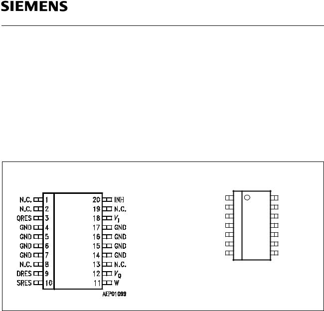
Pin Configuration
(top view)
TLE 4263 G |
TLE 4263 GM |
|
|
N.C. |
1 |
14 |
INH |
QRES |
2 |
13 |
VΙ |
GND |
3 |
12 |
GND |
GND |
4 |
11 |
GND |
GND |
5 |
10 |
GND |
DRES |
6 |
9 |
VQ |
SRES |
7 |
8 |
W |
|
|
AEP02587 |
|
Semiconductor Group |
2 |
1998-11-01 |

TLE 4263
Pin Definitions and Functions
Pin |
Symbol |
Function |
|
|
|
1, 2, 19, 13 |
N.C. |
Not connected |
|
|
|
3 |
QRES |
Reset output; open-collector output connected to the |
|
|
output via a resistor of 30 kΩ. |
|
|
|
4-7, |
GND |
Ground |
14-17 |
|
|
|
|
|
9 |
DRES |
Reset delay; connected to ground with a capacitor. |
|
|
|
10 |
SRES |
Reset threshold; for setting the switching threshold |
|
|
connect with a voltage divider from output to ground. If this |
|
|
input is connected to GND, reset is triggered at an output |
|
|
voltage of 4.5 V. |
|
|
|
11 |
W |
Watchdog; positive edge triggered input for monitoring a |
|
|
microcontroller. |
|
|
|
12 |
VQ |
5-V output voltage; block to ground with a 22−µF |
|
|
capacitor. |
|
|
|
18 |
VI |
Input voltage; block to ground directly at the IC with a |
|
|
ceramic capacitor. |
|
|
|
20 |
INH |
Inhibit; TTL-compatible, low-active input. |
|
|
|
Semiconductor Group |
3 |
1998-11-01 |
|
|

TLE 4263
Circuit Description
The control amplifier compares a reference voltage, which is kept highly accurate by resistance adjustment, to a voltage that is proportional to the output voltage and drives the base of the series transistor via a buffer. Saturation control as a function of the load current prevents any over-saturation of the power element. If the externally scaled down output voltage at the reset threshold input drops below 1.35 V, the external reset delay capacitor is discharged by the reset generator. If the voltage on the capacitor reaches the lower threshold VST, a reset signal is issued on the reset output and not cancelled again until the upper threshold VdT is exceeded. If the reset threshold input is connected to GND, reset is triggered at an output voltage of 4.5 V. A connected microcontroller is controlled by the watchdog logic. If pulses are missing, the reset output is set to low. The pulse sequence time can be set within a wide range with the reset delay capacitor. The IC can be switched at the TTL-compatible, low-active inhibit input. The IC also incorporates a number of internal circuits for protection against:
●Overload
●Overtemperature
●Reverse polarity
|
|
|
11 |
|
|
Temperature |
|
Saturation |
|
|
|
Sensor |
|
Control and |
Watchdog |
|
|
|
Protection |
|
|
||
|
|
|
|
|
|
|
|
Circuit |
|
|
|
18 |
|
|
|
12 |
Output |
Input |
|
|
|
|
|
|
Control |
|
|
9 |
Reset |
|
Amplifier |
Buffer |
|
||
|
|
|
|
Delay |
|
Bandgap |
|
|
|
|
|
|
|
Reset |
3 |
Reset |
|
Reference |
|
|
|||
|
|
Generator |
|
Output |
|
|
|
|
10 |
||
|
|
|
|
Reset |
|
|
|
|
|
|
Threshold |
Adjustment |
|
|
|
|
|
|
|
20 |
4-7, 14-17 |
|
|
|
|
Inhibit |
GND |
|
AEB01100 |
Block Diagram
Semiconductor Group |
4 |
1998-11-01 |

TLE 4263
Absolute Maximum Ratings
Tj = – 40 to 150 °C
Parameter |
Symbol |
Limit Values |
Unit |
Remarks |
|
|
|
|
|
|
|
|
|
|
|
|
|
min. |
max. |
|
|
|
|
|
|
|
|
|
|
|
|
Input |
|
|
|
|
|
|
|
|
|
|
|
|
|
|
|
Input voltage |
VI |
– 42 |
45 |
V |
– |
|
|
Input current |
II |
– |
– |
– |
internally limited |
|
|
Reset Output |
|
|
|
|
|
|
|
|
|
|
|
|
|
|
|
Voltage |
VR |
– 0.3 |
42 |
V |
– |
|
|
Current |
IR |
– |
– |
– |
internally limited |
|
|
Reset Input |
|
|
|
|
|
|
|
|
|
|
|
|
|
|
|
Reset threshold |
VRE |
– 0.3 |
6 |
V |
– |
|
|
Reset Delay |
|
|
|
|
|
|
|
|
|
|
|
|
|
|
|
Voltage |
Vd |
– 0.3 |
42 |
V |
– |
|
|
Current |
Id |
– |
– |
– |
internally limited |
|
|
|
|
|
|
|
|
|
|
Output |
|
|
|
|
|
|
|
|
|
|
|
|
|
|
|
Voltage |
VQ |
– 0.3 |
7 |
V |
– |
|
|
|
|||||||
Current |
IQ |
– |
– |
– |
internally limited |
|
|
|
|
|
|
|
|
|
|
Inhibit |
|
|
|
|
|
|
|
|
|
|
|
|
|
|
|
Voltage |
Ve |
– 42 |
45 |
V |
– |
|
|
|
|
|
|
|
|
|
|
Watchdog |
|
|
|
|
|
|
|
|
|
|
|
|
|
|
|
|
|
|
|
|
|
|
|
Voltage |
VW |
– 0.3 |
6 |
V |
– |
|
|
|
|
|
|
|
|
|
|
Ground |
|
|
|
|
|
|
|
|
|
|
|
|
|
|
|
Current |
IGND |
– 0.5 |
– |
A |
– |
|
|
Semiconductor Group |
|
5 |
|
|
1998-11-01 |
|
|
 Loading...