


TLE 4267
5-V Low-Drop Voltage Regulator |
TLE 4267 |
Bipolar IC
Features
●Output voltage tolerance ≤ ± 2 %
●Low-drop voltage
●Very low standby current consumption
●Input voltage up to 40 V
●Overvoltage protection up to 60 V (≤ 400 ms)
●Reset function down to 1 V output voltage
●ESD protection up to 2000 V
●Adjustable reset time
●On/off logic
●Overtemperature protection
●Reverse polarity protection
●Short-circuit proof
●Wide temperature range
●Suitable for use in automotive electronics
Type |
Ordering Code |
Package |
|
|
|
TLE 4267 |
Q67000-A9153 |
P-TO220-7-3 |
|
|
|
TLE 4267 G |
Q67006-A9169 |
P-TO220-7-180 (SMD) |
TLE 4267 S |
Q67000-A9246 |
P-TO220-7-230 |
|
|
|
Functional Description
P-TO220-7-3 |
P-TO220-7-180 |
P-TO220-7-230 |
TLE 4267 is a 5-V low-drop voltage regulator in a
TO220-7 package. It supplies an output current of > 400 mA. The IC is shortcircuit-proof and incorporates temperature protection that disables the IC at overtemperature.
Application
The IC regulates an input voltage VI in the range 5.5 V < VI < 40 V to VQrated = 5.0 V. A reset signal is generated for an output voltage VQ of < 4.5 V. The reset delay can be set
with an external capacitor. The device has two logic inputs. It is turned-ON by a voltage of > 4 V on E2 by the ignition for example. It remains active as a function of the voltage on E6, even if the voltage on E2 goes Low. This makes it possible to implement a selfholding circuit without external components. When the device is turned-OFF, the output voltage drops to 0 V and current consumption tends towards 0 A.
Semiconductor Group |
1 |
1998-11-01 |

TLE 4267
Design Notes for External Components
The input capacitor CI is necessary for compensation line influences. The resonant circuit consisting of lead inductance and input capacitance can be damped by a resistor of approx. 1 Ω in series with CI. The output capacitor is necessary for the stability of the regulating circuit. Stability is guaranteed at values of ≥ 22 µF and an ESR of ≤ 3 Ω within the operating temperature range.
Circuit Description
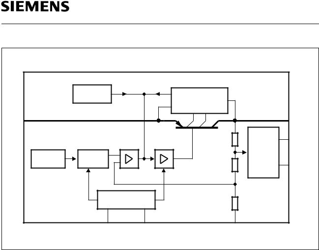
The control amplifier compares a reference voltage, which is kept highly accurate by resistance adjustment, to a voltage that is proportional to the output voltage and drives the base of the series transistor via a buffer. Saturation control as a function of the load current prevents any over-saturating of the power element.
A comparator in the reset-generator block compares a reference that is independent of the input voltage to the scaled-down output voltage. If this reaches a value of 4.5 V, the reset-delay capacitor is discharged and then the reset output is set Low. As the output voltage increases again, the reset-delay capacitor is charged with constant current from VQ = 4.5 V onwards. When the capacitor voltage reaches the upper switching threshold, reset goes High again. The reset delay can be set within wide range by selection of the external capacitor.
With the integrated turn-ON/turn-OFF logic it is simple to implement delayed turn-OFF without external components.
Truth Table for Turn-ON/Turn-OFF Logic
Pin 2 |
Pin 6 |
VQ |
Remarks |
|
|
|
|
|
|
|
|
L |
X |
OFF |
Initial state, pin 6 internally pulled up |
|
|
|
|
|
|
|
|
H |
X |
ON |
Regulator switched on via pin 2, by ignition for example |
|
|
|
|
|
|
|
|
H |
L |
ON |
Pin 6 clamped active to ground by controller while pin 2 is still |
|
|
|
|
|
high |
|
|
|
|
|
|
|
|
X |
L |
ON |
Previous state remains, even ignition is shut off: self-holding |
|
|
|
|
|
state |
|
|
|
|
|
|
|
|
L |
L |
ON |
Ignition shut off while regulator is in self-holding state |
|
|
|
|
|
|
|
|
L |
H |
OFF |
Regulator shut down by releasing of pin 6 while pin 2 remains |
|
|
|
|
|
Low, final state. No active clamping required by external self- |
|
|
|
|
|
holding circuit (µC) to keep regulator shut off. |
|
|
|
|
|
|
|
|
Pin 2: (Inhibit, E2) Enable function, active High
Pin 6: (Hold, E6) Hold and release function, active Low
Semiconductor Group |
2 |
1998-11-01 |

TLE 4267
Pin Configuration
(top view)
P-TO220-7-3 |
P-TO220-7-180 |
P-TO220-7-230 |
1 2 3 4 5 6 7
1 2 3 4 5 6 7
1 2 3 4 5 6 7 |
Ι |
R |
D |
|
E2 |
GND |
E6 |
AEP01724
|
|
|
|
|
Ι |
R |
D |
Q |
Ι |
R |
D |
Q |
E2 |
GND |
|
E6 |
|
E2 |
GND |
|
E6 |
|
|
|
AEP02123 |
|
|
|
|
AEP01481 |
|
|
|
|
|
|
|
|
|
|||||
Pin Definitions and Functions |
|
|
|
|||||
|
|
|
|
|
|
|
||
Pin |
Symbol |
|
Function |
|
|
|
||
|
|
|
|
|
|
|||
1 |
I |
|
|
|
Input; block to ground directly at the IC by a ceramic capacitor |
|||
|
|
|
|
|
|
|||
2 |
E2 |
|
|
|
Inhibit; device is turned-ON by High signal on this pin; internal |
|||
|
|
|
|
|
pulldown resistor of 100 kΩ |
|
|
|
|
|
|
|
|
|
|||
3 |
R |
|
|
|
Reset Output; open-collector output internally connected to |
|||
|
|
|
|
|
the output via a resistor of 30 kΩ |
|
|
|
|
|
|
|
|
|
|
|
|
4 |
GND |
|
|
Ground; connected to rear of chip |
|
|
|
|
|
|
|
|
|
|
|||
5 |
D |
|
|
|
Reset Delay; connect with capacitor to GND for setting delay |
|||
|
|
|
|
|
|
|||
6 |
E6 |
|
|
|
Hold; see truth table above for function; this input is connected |
|||
|
|
|
|
|
to output voltage across pullup resistor of 50 kΩ |
|
|
|
|
|
|
|
|
|
|||
7 |
Q |
|
|
|
5-V Output; block to GND with 22-µF capacitor, ESR < 3 Ω |
|||
|
|
|
|
|
|
|
|
|
Semiconductor Group |
3 |
1998-11-01 |
TLE 4267
|
|
Temperature |
|
|
Saturation |
|
|
|
Sensor |
|
|
|
|
|
|
|
|
Control and |
|
|
|
|
|
|
|
|
|
|
|
|
|
|
Protection Circuit |
|
In- |
1 |
|
|
|
7 |
5 V |
put |
|
|
|
|
|
Output |
|
|
|
Control |
|
5 |
Reset |
|
|
|
Amplifier |
Buffer |
Reset |
Delay |
|
|
Bandgap |
|
|
|
|
|
Adjustment |
|
|
Generator |
|
|
|
Reference |
|
|
3 |
Reset |
|
|
|
|
|
|||
|
|
|
|
|
|
Output |
|
|
Turn-ON/Turn-OFF |
|
|
|
|
|
|
|
Logic |
|
|
|
|
|
2 |
6 |
|
4 |
|
|
|
Inhibit |
E6 Hold |
|
GND |
AEB01482 |
Block Diagram
Absolute Maximum Ratings
TJ = – 40 to 150 °C
Parameter |
Symbol |
Limit Values |
Unit |
Notes |
|
|
|
|
|
|
|
|
|
|
|
|
|
min. |
max. |
|
|
|
|
Input |
|
|
|
|
|
|
|
|
|
|
|
|
|
|
|
Voltage |
VI |
– 42 |
42 |
V |
– |
|
|
|
|
|
|
|
|
|
|
Voltage |
VI |
– |
60 |
V |
t ≤ 400 ms |
|
|
|
|
|
|
|
|
|
|
Current |
II |
– |
– |
– |
Limited internally |
|
|
|
|
|
|
|
|
|
|
Reset Output |
|
|
|
|
|
|
|
|
|
|
|
|
|
|
|
|
|
|
|
|
|
|
|
Voltage |
VR |
– 0.3 |
7 |
V |
– |
|
|
Current |
IR |
– |
– |
– |
Limited internally |
|
|
Reset Delay |
|
|
|
|
|
|
|
|
|
|
|
|
|
|
|
Voltage |
Vd |
– 0.3 |
42 |
V |
– |
|
|
Semiconductor Group |
4 |
1998-11-01 |

TLE 4267
Absolute Maximum Ratings (cont’d)
TJ = – 40 to 150 °C
Parameter |
Symbol |
Limit Values |
Unit |
Notes |
|
|
|
|
|
|
|
|
|
min. |
max. |
|
|
|
|
|
|
|
|
Current |
Id |
– |
– |
– |
– |
|
|
|
|
|
|
Output |
|
|
|
|
|
|
|
|
|
|
|
Voltage |
VQ |
– 0.3 |
7 |
V |
– |
Current |
IQ |
– |
– |
– |
Limited internally |
|
|
|
|
|
|
Inhibit |
|
|
|
|
|
|
|
|
|
|
|
Voltage |
VE2 |
– 42 |
42 |
V |
|
Current |
IE2 |
– 5 |
5 |
mA |
t ≤ 400 ms |
Hold |
|
|
|
|
|
|
|
|
|
|
|
Voltage |
VE6 |
– 0.3 |
7 |
V |
– |
Current |
IE6 |
– |
– |
mA |
Limited internally |
GND |
|
|
|
|
|
|
|
|
|
|
|
Current |
IGND |
– 0.5 |
– |
A |
– |
Temperatures |
|
|
|
|
|
|
|
|
|
|
|
Junction temperature |
TJ |
– |
150 |
°C |
– |
|
|
|
|
|
|
Storage temperature |
Tstg |
– 50 |
150 |
°C |
– |
Operating Range |
|
|
|
|
|
|
|
|
|
|
|
Parameter |
Symbol |
Limit Values |
Unit |
Notes |
|
|
|
|
|
|
|
|
|
min. |
max. |
|
|
|
|
|
|
|
|
Input voltage |
VI |
5.5 |
40 |
V |
see diagram |
|
|
|
|
|
|
Junction temperature |
TJ |
– 40 |
150 |
°C |
– |
|
|
|
|
|
|
Thermal Resistance |
|
|
|
|
|
|
|
|
|
|
|
Junction ambient |
Rthja |
– |
70 |
K/W |
– |
Junction-case |
Rthjc |
– |
6 |
K/W |
– |
Junction-case |
Rthjc |
– |
2 |
K/W |
t < 1 ms |
Semiconductor Group |
5 |
1998-11-01 |
 Loading...