


Philips HEF40106BDB, HEF40106BD, HEF40106BU, HEF40106BT, HEF40106BPB Datasheet
...INTEGRATED CIRCUITS
DATA SHEET
For a complete data sheet, please also download:
∙The IC04 LOCMOS HE4000B Logic Family Specifications HEF, HEC
∙The IC04 LOCMOS HE4000B Logic Package Outlines/Information HEF, HEC
HEF40106B gates
Hex inverting Schmitt trigger
Product specification |
|
January 1995 |
|||||
File under Integrated Circuits, IC04 |
|
|
|
|
|
|
|
|
|
|
|
|
|
|
|
|
|
|
|
|
|
|
|
|
|
|
|
|
|
|
|

Philips Semiconductors |
Product specification |
|
|
Hex inverting Schmitt trigger
HEF40106B gates
DESCRIPTION
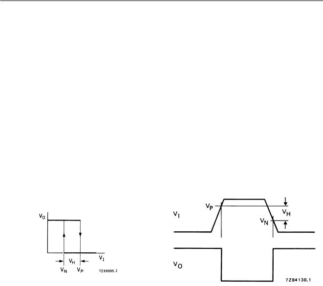
Each circuit of the HEF40106B functions as an inverter with Schmitt-trigger action. The Schmitt-trigger switches at different points for the positive and negative-going input signals. The difference between the positive-going voltage (VP) and the negative-going voltage (VN) is defined as hysteresis voltage (VH).
This device may be used for enhanced noise immunity or to “square up” slowly changing waveforms.
Fig.2 Pinning diagram.
HEF40106BP(N): 14-lead DIL; plastic (SOT27-1)
HEF40106BD(F): 14-lead DIL; ceramic (cerdip) (SOT73)
HEF40106BT(D): 14-lead SO; plastic (SOT108-1)
( ): Package Designator North America
Fig.1 Functional diagram.
Fig.3 Logic diagram (one inverter).
FAMILY DATA, IDD LIMITS category GATES
See Family Specifications
January 1995 |
2 |
Philips Semiconductors Product specification
Hex inverting Schmitt trigger |
|
|
|
HEF40106B |
||
|
|
|
|
gates |
||
|
|
|
|
|
|
|
|
|
|
|
|
|
|
DC CHARACTERISTICS |
|
|
|
|
|
|
VSS = 0 V; Tamb = 25 °C |
|
|
|
|
|
|
|
|
|
|
|
|
|
|
VDD |
SYMBOL |
MIN. |
TYP. |
MAX. |
|
|
V |
|
||||
|
|
|
|
|
|
|
|
|
|
|
|
|
|
Hysteresis |
5 |
|
0,5 |
0,8 |
|
V |
voltage |
10 |
VH |
0,7 |
1,3 |
|
V |
|
15 |
|
0,9 |
1,8 |
|
V |
|
|
|
|
|
|
|
Switching levels |
5 |
|
2 |
3,0 |
3,5 |
V |
positive-going |
10 |
VP |
3,7 |
5,8 |
7 |
V |
input voltage |
15 |
|
4,9 |
8,3 |
11 |
V |
|
|
|
|
|
|
|
negative-going |
5 |
|
1,5 |
2,2 |
3 |
V |
input voltage |
10 |
VN |
3 |
4,5 |
6,3 |
V |
|
15 |
|
4 |
6,5 |
10,1 |
V |
|
|
|
|
|
|
|
|
|
Fig.5 |
Waveforms showing definition of |
Fig.4 Transfer characteristic. |
|
|
VP, VN and VH, where VN and VP are |
|
|
between limits of 30% and 70%. |
|
|
|
|
|
January 1995 |
3 |
 Loading...