

Motorola MC74HC147N, MC74HC147D Datasheet
SEMICONDUCTOR TECHNICAL DATA
1
REV 6
Motorola, Inc. 1995
10/95
High–Performance Silicon–Gate CMOS
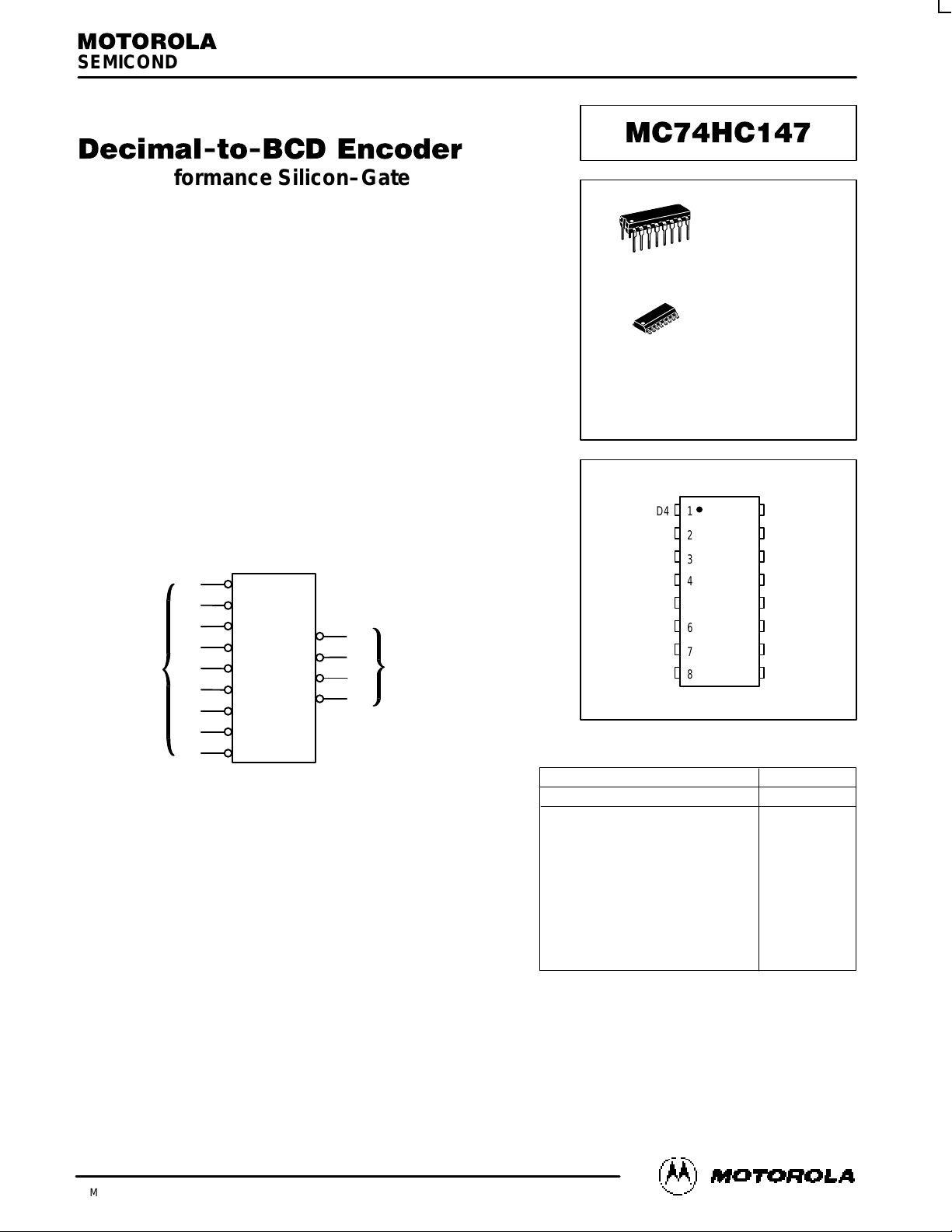
The MC74HC147 is identical in pinout to the LS147. The device inputs are
compatible with standard CMOS outputs; with pullup resistors, they are
compatible with LSTTL outputs.
This device encodes nine active–low data inputs to four active–low BCD
Address Outputs, ensuring that only the highest order active data line is
encoded. The implied decimal zero condition is encoded when all nine data
inputs are at a high level (inactive).
• Output Drive Capability: 10 LSTTL Loads
• Outputs Directly Interface to CMOS, NMOS, and TTL
• Operating Voltage Range: 2 to 6 V
• Low Input Current: 1 µA
• High Noise Immunity Characteristic of CMOS Devices
• In Compliance with the Requirements Defined by JEDEC Standard
No. 7A
• Chip Complexity: 136 FETs or 34 Equivalent Gates
LOGIC DIAGRAM
DECIMAL
DATA INPUTS
(ACTIVE–LOW)
BCD
ADDRESS
OUTPUTS
(ACTIVE–LOW)
A0
A1
A2
A3
D1
D2
D3
D4
D5
D6
D7
D8
D9
11
12
13
1
2
3
4
5
10
9
7
6
14
VCC= PIN 16
GND = PIN 8
NO CONNECTION = PIN 15
PIN ASSIGNMENT
13
14
15
16
9
10
11
125
4
3
2
1
8
7
6
D4
D7
D6
D5
A1
A2
D8
GND
D2
D3
A3
NC
V
CC
D9
D1
A0
NC = NO CONNECTION
D SUFFIX
SOIC PACKAGE
CASE 751B–05
N SUFFIX
PLASTIC PACKAGE
CASE 648–08
1
16
1
16
ORDERING INFORMATION
MC74HCXXXN
MC74HCXXXD
Plastic
SOIC
Inputs Outputs
D9 D8 D7 D6 D5 D4 D3 D2 D1 A3 A2 A1 A0
H H H H H H H H H H H H H
H H H H H H H H L H H H L
H H H H H H H L X H H L H
H H H H H H L X X H H L L
H H H H H L X X X H L H H
H H H H L X X X X H L H L
H H H L X X X X X H L L H
H H L X X X X X X H L L L
H L X X X X X X X L H H H
L X X X X X X X X L H H L
FUNCTION TABLE
MC74HC147
MOTOROLA High–Speed CMOS Logic Data
DL129 — Rev 6
2
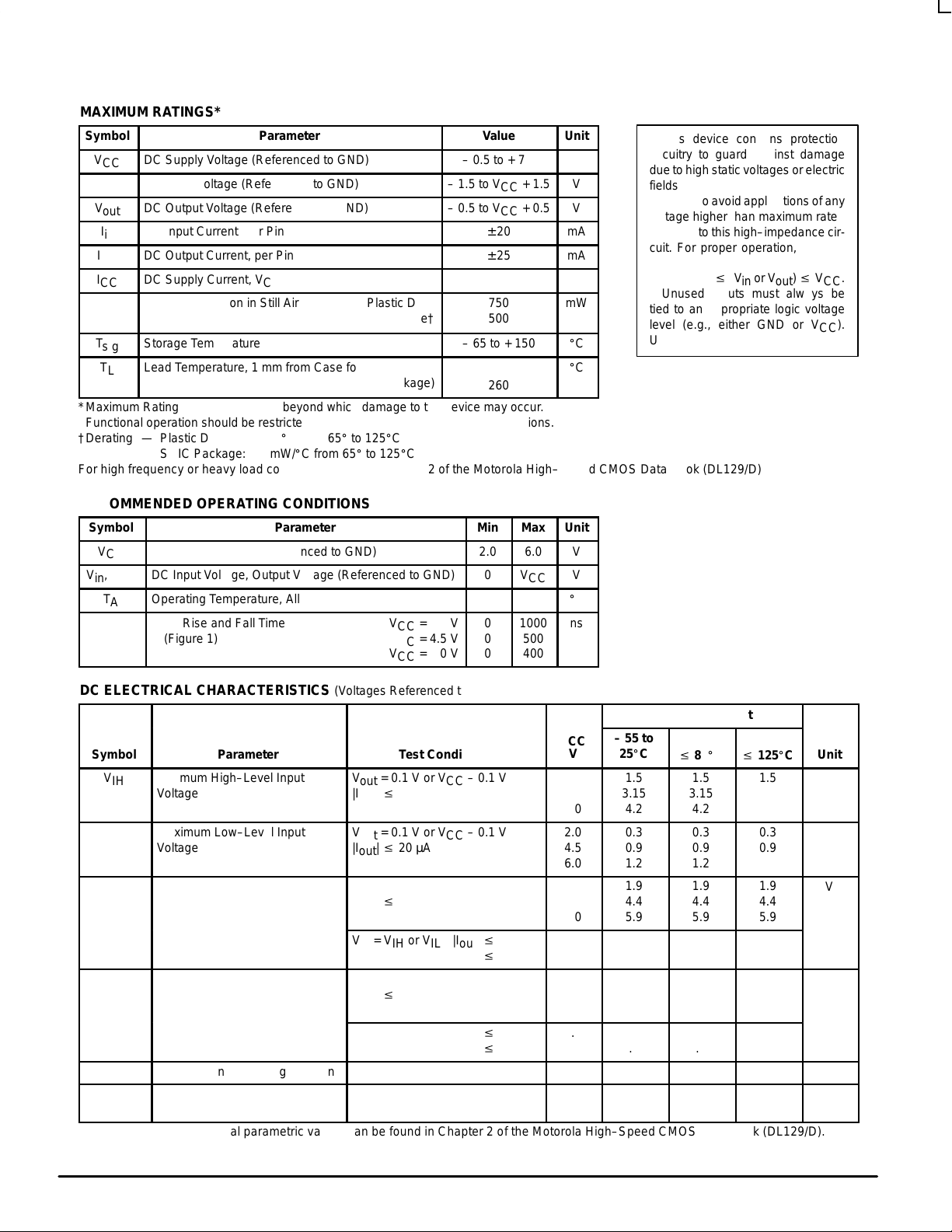
MAXIMUM RATINGS*
Symbol
Parameter
Value
Unit
V
CC
DC Supply Voltage (Referenced to GND)
– 0.5 to + 7.0
V
V
in
DC Input Voltage (Referenced to GND)
– 1.5 to VCC + 1.5
V
V
out
DC Output Voltage (Referenced to GND)
– 0.5 to VCC + 0.5
V
I
in
DC Input Current, per Pin
± 20
mA
I
out
DC Output Current, per Pin
± 25
mA
I
CC
DC Supply Current, VCC and GND Pins
± 50
mA
P
D
Power Dissipation in Still Air Plastic DIP†
SOIC Package†
750
500
mW
T
stg
Storage Temperature
– 65 to + 150
_
C
T
L
Lead Temperature, 1 mm from Case for 10 Seconds
(Plastic DIP or SOIC Package)
260
_
C
*Maximum Ratings are those values beyond which damage to the device may occur.
Functional operation should be restricted to the Recommended Operating Conditions.
†Derating — Plastic DIP: – 10 mW/_C from 65_ to 125_C
SOIC Package: – 7 mW/_C from 65_ to 125_C
For high frequency or heavy load considerations, see Chapter 2 of the Motorola High–Speed CMOS Data Book (DL129/D).
RECOMMENDED OPERATING CONDITIONS
Symbol
Parameter
Min
Max
Unit
V
CC
DC Supply Voltage (Referenced to GND)
2.0
6.0
V
Vin, V
out
DC Input Voltage, Output Voltage (Referenced to GND)
0
V
CC
V
T
A
Operating Temperature, All Package Types
– 55
+ 125
_
C
tr, t
f
Input Rise and Fall Time VCC = 2.0 V
(Figure 1) VCC = 4.5 V
VCC = 6.0 V
0
0
0
1000
500
400
ns
DC ELECTRICAL CHARACTERISTICS (Voltages Referenced to GND)
Guaranteed Limit
Symbol
Parameter
Test Conditions
V
CC
V
– 55 to
25_C
v
85_C
v
125_C
Unit
V
IH
Minimum High–Level Input
Voltage
V
out
= 0.1 V or VCC – 0.1 V
|I
out
| v 20 µA
2.0
4.5
6.0
1.5
3.15
4.2
1.5
3.15
4.2
1.5
3.15
4.2
V
V
IL
Maximum Low–Level Input
Voltage
V
out
= 0.1 V or VCC – 0.1 V
|I
out
| v 20 µA
2.0
4.5
6.0
0.3
0.9
1.2
0.3
0.9
1.2
0.3
0.9
1.2
V
Vin = VIH or V
IL
|I
out
| v 20 µA
2.0
4.5
6.0
1.9
4.4
5.9
1.9
4.4
5.9
1.9
4.4
5.9
Vin = VIH or VIL|I
out
| v 4.0 mA
|I
out
| v 5.2 mA
4.5
6.0
3.98
5.48
3.84
5.34
3.70
5.20
Vin = V
IH
|I
out
| v 20 µA
2.0
4.5
6.0
0.1
0.1
0.1
0.1
0.1
0.1
0.1
0.1
0.1
Vin = VIH or VIL|I
out
| v 4.0 mA
|I
out
| v 5.2 mA
4.5
6.0
0.26
0.26
0.33
0.33
0.40
0.40
I
in
Maximum Input Leakage Current
Vin = VCC or GND
6.0
± 0.1
± 1.0
± 1.0
µA
I
CC
Maximum Quiescent Supply
Current (per Package)
Vin = VCC or GND
I
out
= 0 µA
6.0
8
80
160
µA
NOTE: Information on typical parametric values can be found in Chapter 2 of the Motorola High–Speed CMOS Data Book (DL129/D).
This device contains protection
circuitry to guard against damage
due to high static voltages or electric
fields. However, precautions must
be taken to avoid applications of any
voltage higher than maximum rated
voltages to this high–impedance circuit. For proper operation, Vin and
V
out
should be constrained to the
range GND v (Vin or V
out
) v VCC.
Unused inputs must always be
tied to an appropriate logic voltage
level (e.g., either GND or VCC).
Unused outputs must be left open.
V
OH
V
OL
Minimum High–Level Output
Voltage
Maximum Low–Level Output
Voltage
V
V
 Loading...