


Motorola MC10195P, MC10195FN, MC10195L Datasheet
SEMICONDUCTOR TECHNICAL DATA
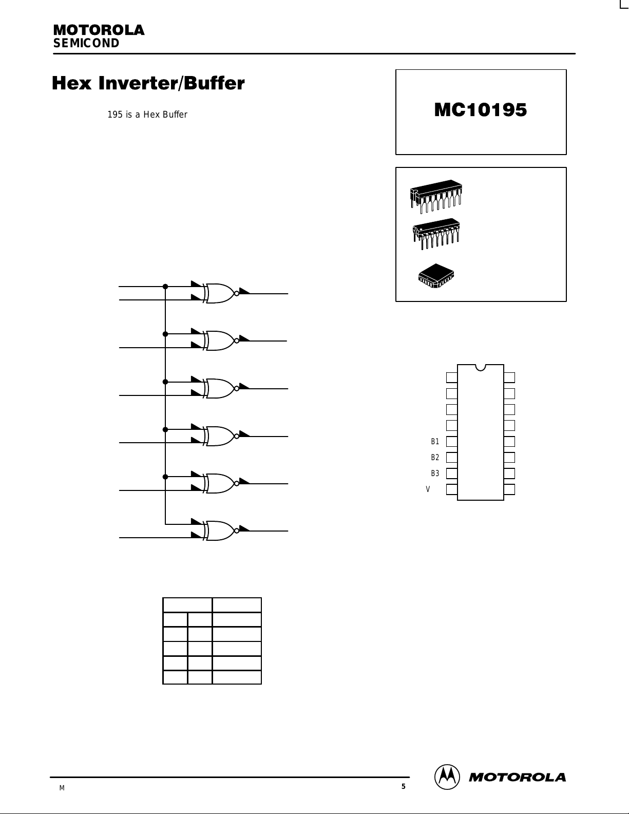
The MC10195 is a Hex Buffer Inverter which is built using six EXCLUSIVE
NOR gates. There is a common input to these gates which when placed low or
left open allows them to act as inverters. With the common input connected to
a high logic level the MC10195 is a hex buffer, useful for high fanout clock
driving and reducing stub lengths on long bus lines.
PD= 200 mW typ/pkg (No Load)
tpd= 2.8 ns typ (B–Q)
tpd= 3.8 ns typ (A–Q)
tr, tf= 2.5 ns typ (20%–80%)
LOGIC DIAGRAM
A
10
9
B
5
6
7
11
Q
2
3
4
13
14
CERAMIC PACKAGE
CASE 620–10
PLASTIC PACKAGE
CASE 648–08
CASE 775–02
DIP
PIN ASSIGNMENT
16
V
CC1
Q1
Q2
Q3
B1
B2
B3
V
EE
1
15
2
14
3
13
4
12
5
11
6
10
7
8
L SUFFIX
P SUFFIX
FN SUFFIX
PLCC
V
Q6
Q5
Q4
B6
B5
B4
A
9
CC2
12
3/93
Motorola, Inc. 1996
TRUTH TABLE
Inputs
A B Q
L L H
L H L
H L L
H H H
Output
3–164
15
V
= PIN 1
CC1
V
= PIN 16
CC2
VEE= PIN 8
Pin assignment is for Dual–in–Line Package.
For PLCC pin assignment, see the Pin Conversion
Tables on page 6–36 of the Motorola MECL Data
Book (DL122/D).
REV 5
MC10195
Under
Und
(VCC)
ELECTRICAL CHARACTERISTICS
Test Limits
Pin
Characteristic Symbol
Power Supply Drain Current I
Input Current I
Output Voltage Logic 1 V
Output Voltage Logic 0 V
Threshold Voltage Logic 1 V
Threshold Voltage Logic 0 V
Switching Times (50Ω Load) ns
Propagation Delay t
Rise Time (20 to 80%) t
Fall Time (20 to 80%) t
E
inH
I
inL
OH
OL
OHA
OLA
5+2–
t
7–4+
t
10+13+
t
11–14–
t
9–14–
2+
2–
Under
Test
8 54 39 49 54 mAdc
5
9
5 0.5 0.5 0.3 µAdc
2 –1.060 –0.890 –0.960 –0.810 –0.890 –0.700 Vdc
2 –1.890 –1.675 –1.850 –1.650 –1.825 –1.615 Vdc
2 –1.080 –0.980 –0.910 Vdc
2 –1.655 –1.630 –1.595 Vdc
2
4
13
14
14
2 1.1 4.7 1.1 2.5 4.5 1.1 5.0
2 1.1 4.7 1.1 2.5 4.5 1.1 5.0
–30°C +25°C +85°C
Min Max Min Typ Max Min Max
1.1
1.1
1.1
1.1
1.1
425
460
4.2
4.2
4.2
4.2
5.2
1.1
1.1
1.1
1.1
1.1
2.8
2.8
2.8
2.8
3.8
265
290
4.0
4.0
4.0
4.0
5.0
1.1
1.1
1.1
1.1
1.1
265
290
4.4
4.4
4.4
4.4
5.4
Unit
µAdc
ELECTRICAL CHARACTERISTICS (continued)
TEST VOLTAGE VALUES (Volts)
@ Test Temperature V
–30°C –0.890 –1.890 –1.205 –1.500 –5.2
+25°C –0.810 –1.850 –1.105 –1.475 –5.2
+85°C –0.700 –1.825 –1.035 –1.440 –5.2
Pin
Characteristic Symbol
Power Supply Drain Current I
Input Current I
Output Voltage Logic 1 V
Output Voltage Logic 0 V
Threshold Voltage Logic 1 V
Threshold Voltage Logic 0 V
Switching Times (50Ω Load) Pulse In Pulse Out –3.2 V +2.0 V
Propagation Delay t
Rise Time (20 to 80%) t
Fall Time (20 to 80%) t
Each MECL 10,000 series circuit has been designed to meet the dc specifications shown in the test table, after thermal equilibrium has been
established. The circuit is in a test socket or mounted on a printed circuit board and transverse air flow greater than 500 linear fpm is maintained.
Outputs are terminated through a 50–ohm resistor to –2.0 volts. Test procedures are shown for only one gate. The other gates are tested in the
same manner.
E
inH
I
inL
OH
OL
OHA
OLA
5+2–
t
7–4+
t
10+13+
t
11–14–
t
9–14–
2+
2–
er
Test
8 8 1, 16
5
9
5 5 8 1, 16
2 8 1, 16
2 9 8 1, 16
2 5 8 1, 16
2 5 8 1, 16
2
4
13
14
14
2 5 2 8 1, 16
2 5 2 8 1, 16
IHmax
TEST VOLTAGE APPLIED TO PINS LISTED BELOW
V
IHmax
5
9
V
ILmin
V
ILmin
V
IHAminVILAmax
V
IHAminVILAmax
5
7
10
11
9
2
4
13
14
14
V
EE
V
EE
8
8
8
8
8
8
8
Gnd
1, 16
1, 16
1, 16
1, 16
1, 16
1, 16
1, 16
DL122 — Rev 6
3–165 MOTOROLAMECL Data
 Loading...