


FEATURES
•Dot Matrix Replacement for DL1414T
•0.145" High, Dot Matrix Character
•128 Special ASCII Characters for English, German, Italian, Swedish, Danish, and Norwegian Languages
•Wide Viewing Angle: X Axis ±50°, Y Axis ±75°
•Close Vertical Row Spacing, 0.800" Centers
•Fast Access Time, 110 ns at 25°C
•Compact Size for Hand Held Equipment
•Builtin Memory
•Built-in Character Generator
•Built-in Multiplex and LED Drive Circuitry
•Direct Access to Each Digit Independently and Asynchronously
•TTL Compatible, 5 Volt Power
•Low Power Consumption, 20 mA per Character Typical
•Intensity Coded for Display Uniformity
•Extended Operating Temperature Range: –40°C to +85°C
•End Stackable, 4-Character Package
RED DLR1414
HIGH EFFICIENCY RED DLO1414
GREEN DLG1414
.145" 4-character 5 x 7 Dot Matrix Alphanumeric Intelligent Display with Memory/Decoder/Driver
Dimensions in inches (mm) |
|
|
.240 |
|
|
|
|
|
|
.0920 |
|
|
|
.0200 (.51) |
.1750 |
|
(6.10) |
|
.012 (.30) |
|
|
(4.45) |
|
(2.34) |
ref. |
|
± .002 (.05) |
|
|
|
|
|
|
12 pl. |
|
|
|
|
.800 |
.600±.020 |
|
|
|
|
|
(20.32) |
||
.0220 |
|
|
|
max. |
(15.24±.51) |
|
(.56) |
|
|
|
|
|
|
|
|
|
.1440 |
|
|
|
|
|
|
(3.66) |
|
|
|
|
.700 max. |
|
|
.210 |
|
|
|
|
|
(5.33) |
|
||
|
(17.78) |
|
|
|
|
|
|
|
|
|
|
|
|
|
|
Luminous |
|
.010 (.25) 4 pl. |
|
|
Part Number |
Intensity |
|
|
|
||
|
|
|
|
|||
Code |
|
.070 (1.78) ± .003 (.08) 4 |
pl. |
|||
|
|
|
||||
Pin Indicator |
DLX 1414 |
|
|
|
|
|
.050 (1.27) 4 pl. |
|
.240 (6.10) |
|
|
||
SIEMENS YYWW |
Z |
|
|
|||
|
|
|
|
|||
.160±.020 |
|
|
|
|
|
|
(4.06±.51) |
|
|
|
EIA Date Code |
|
|
|
|
|
|
.100 (2.54) 10 pl. |
|
|
.095 (2.41) |
|
|
|
at Seating Plane |
|
|
|
.018 (.46) 12 pl. |
|
|
|||
ref. |
|
|
|
|||
|
|
|
Tolerance: XXX± .01 (.254) |
|||
|
|
|
|
|||
DESCRIPTION
The DLR/DLO/DLG1414 is a four digit 5x7 dot matrix display module with a built-in CMOS integrated circuit. This display is a drop-in dot matrix replacement for the DL1414T with segmented characters.
The integrated circuit contains memory, ASCII ROM decoder, multiplex circuitry and drivers. Data entry is asynchronous and random. A display system can be built using any number of DLX1414s since each character in any DLX1414 can be addressed independently and will continue to display the character last stored until replaced by another.
System interconnection is very straightforward. The least significant two address bits (A0, A1) are normally connected to the like named inputs of all displays in the system. Data lines are connected to all DLX1414s directly and in parallel as is the write line (WR). The display then will behave as a write only memory.
The DLX1414 has several features superior to competitive devices. The character set consists of 128 special ASCII characters for English, German, Italian, Swedish, Danish, and Norwegian.
See Appnotes 18, 19, 22, and 23 for additional information.
2–1
Maximum Ratings |
|
|
DC Supply Voltage ....................... |
|
–0.5 to +7.0 Vdc |
Input Voltage Levels Relative |
|
|
to GND (all inputs) ............. |
–0.5 to VCC +0.5 Vdc |
|
Operating Temperature .................. |
|
–40°C to +85°C |
Storage Temperature.................... |
|
–40°C to +100°C |
Maximum Solder Temperature ........ |
063" (1.59 mm) |
|
below Seating Plane, t<5 sec.................... |
260°C |
|
Relative Humidity at 85°C ................................ |
|
85% |
Optical Characteristics |
|
|
Spectral Peak Wavelength |
|
|
Red ................................................... |
|
660 nm typ. |
High Efficiency Red (HER) ............... |
|
630 nm typ. |
Green................................................ |
|
565 nm typ. |
Viewing Angle (off normal axis) |
|
|
Horizontal..................................................... |
|
± 50° |
Vertical ......................................................... |
|
± 75° |
Character Height........................................... |
|
0.145" |
Time Averaged Luminous Intensity1 |
||
(100% brightness, VCC=5 V) |
50 cd/LED typ. |
|
Red ............................................ |
|
|
HER............................................ |
|
60 cd/LED typ. |
Green......................................... |
|
70 cd/LED typ. |
LED to LED Intensity Matching ........... |
1.8:1.0 max. |
|
LED to LED Hue Matching at VCC=5 V |
||
(Green only) ..................................... |
|
± 2 nm max. |
Note 1: Peak luminous intensity values can be calculated by multiplying these values by 7.
DC Characteristics
Figure 1. Top view
12 11 10 9 8 7
|
|
|
|
|
|
|
|
|
|
|
|
|
|
|
|
|
|
|
|
|
|
|
|
|
|
|
|
|
|
|
|
|
|
|
|
|
|
|
|
|
|
|
|
|
|
|
|
|
|
|
|
|
|
|
|
|
|
|
|
|
|
|
|
|
|
|
|
|
|
|
|
|
|
|
|
|
|
|
|
digit |
digit |
digit |
|
digit |
|
|
|
|
|
|
|
|
|
|
|
|
|
|
|
|
|
|
|
|
|
|
|
|
|
|
||||||
|
3 |
2 |
|
1 |
0 |
|
|
|
|
|
|
|
|
|
|
|
|
|
|
|
|
|
|
|
|
|
|
|
|
|
|
|
||||||
|
|
|
|
|
|
|
|
|
|
|
|
|
|
|
|
|
|
|
|
|
|
|
|
|
|
|
|
|
|
|
|
|
|
|
|
|
|
|
1 |
2 |
3 |
|
4 |
|
5 |
6 |
|
|
|
|
|
|
|
|
|
|
|
|
|
|
|
|
|
|
|
|
|
|
|
|
|
|
|
||||
|
|
|
|
|
|
|
|
|
|
|
|
|
|
|
|
|
|
|
|
|
|
|
|
|
|
|
|
|
|
|
|
|
|
|
|
|||
Pin |
|
|
Function |
|
|
|
|
|
|
|
|
|
|
|
|
|
Pin |
|
Function |
|||||||||||||||||||
|
|
|
|
|
|
|
|
|
|
|
|
|
|
|
|
|
|
|
|
|
|
|
|
|
|
|
|
|
|
|
|
|
|
|
||||
1 |
|
|
|
|
D5 Data Input |
|
|
|
|
|
|
|
|
|
|
7 |
|
|
|
|
|
|
|
GND |
||||||||||||||
|
|
|
|
|
|
|
|
|
|
|
|
|
|
|
|
|
|
|
|
|
|
|
|
|
|
|
|
|
|
|
|
|
|
|
|
|||
2 |
|
|
|
|
D4 Data Input |
|
|
|
|
|
|
|
|
|
|
8 |
|
|
|
|
|
|
|
D0 |
Data Input (LSB) |
|||||||||||||
|
|
|
|
|
|
|
|
|
|
|
|
|
|
|
|
|
|
|
|
|
|
|
|
|
|
|
|
|
|
|
|
|
|
|
|
|
|
|
3 |
|
|
|
|
|
Write |
|
|
|
|
|
|
|
|
|
|
|
|
9 |
|
|
|
|
|
|
|
D1 |
Data Input |
||||||||||
|
|
WR |
|
|
|
|
||||||||||||||||||||||||||||||||
|
|
|
|
|
|
|
|
|
|
|
|
|
|
|
|
|
|
|
|
|
|
|
|
|
|
|
|
|
|
|
|
|
|
|
|
|||
4 |
|
|
|
|
A1 Digit Select |
|
|
|
|
|
|
|
|
10 |
|
|
|
|
|
|
|
D2 |
Data Input |
|||||||||||||||
|
|
|
|
|
|
|
|
|
|
|
|
|
|
|
|
|
|
|
|
|
|
|
|
|
|
|
|
|
|
|
|
|
|
|
|
|||
5 |
|
|
|
|
A0 Digit Select |
|
|
|
|
|
|
|
|
11 |
|
|
|
|
|
|
|
D3 |
Data Input |
|||||||||||||||
|
|
|
|
|
|
|
|
|
|
|
|
|
|
|
|
|
|
|
|
|
|
|
|
|
|
|
|
|
|
|
|
|
|
|
|
|
|
|
6 |
|
|
|
|
VCC |
|
|
|
|
|
|
|
|
|
|
|
|
|
|
12 |
|
|
|
|
|
|
|
D6 |
Data Input (MSB) |
|||||||||
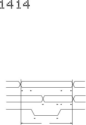
Figure 2. Timing characteristics (VCC=4.5 V) |
|
|
|
|
|
|||||||||||||||||||||||||||||||||
A0, A1 |
|
|
|
|
|
|
|
|
|
|
|
|
|
|
|
|
|
|
|
|
|
|
|
|
|
|
|
|
|
|
|
|
|
|
|
2.0 V |
||
|
|
|
|
|
|
|
|
|
|
|
|
|
|
|
|
|
|
|
|
|
|
|
|
|
|
|
|
|
|
|
|
|
|
|
||||
|
|
|
|
|
|
|
|
|
|
|
|
|
|
|
|
|
|
|
|
|
|
|
|
|
|
|
|
|
|
|
|
|
|
|||||
|
|
|
|
|
|
|
|
|
|
|
|
|
|
|
|
|
|
|
|
|
|
|
|
|
|
|
|
|
|
|
|
|
|
|
0.8 V |
|||
|
|
|
|
|
|
|
|
|
|
TAS |
|
|
|
|
|
|
|
|
|
|
|
|
|
|
|
|
|
|
|
|
TAH |
|
|
|
|
|
||
D0-D6 |
|
|
|
|
|
|
|
|
|
|
|
|
|
|
|
|
|
|
|
|
|
|
|
|
|
|
|
|
|
|
|
|
2.0 V |
|||||
|
|
|
|
|
|
|
|
|
|
|
|
|
|
|
|
|
|
|
|
|
|
|
|
|
|
|
|
|
|
|
|
|||||||
|
|
|
|
|
|
|
|
|
|
|
|
|
|
|
|
|
|
|
|
|
|
|
|
|
|
|
|
|
|
|
|
|
|
|
||||
|
|
|
|
|
|
|
|
|
|
|
|
|
|
|
|
|
|
|
|
|
|
|
|
|
|
|
|
|
|
|
|
|
|
|
||||
|
|
|
|
|
|
|
|
|
|
|
|
|
|
|
|
|
|
|
|
|
|
|
|
|
|
|
|
|
|
|
|
|
|
|||||
|
|
|
|
|
|
|
|
|
|
|
|
|
|
|
|
|
|
|
|
|
|
|
|
|
|
|
|
|
|
|
|
|
|
|
0.8 V |
|||
|
|
|
|
|
|
|
|
|
|
|
|
|
|
|
|
|
|
|
|
TDS |
|
|
|
|
|
|
|
TDH |
|
|
|
|
|
|
||||
|
|
|
|
|
|
|
|
|
|
|
|
|
|
|
|
|
|
|
|
|
|
|
|
|
|
|
|
|
|
|
|
|||||||
|
|
|
|
|
|
|
|
|
|
|
|
|
|
|
|
|
|
|
|
|
|
|
||||||||||||||||
|
|
|
|
|
|
|
|
|
|
|
|
|
|
|
|
|
|
|
|
|
|
|
|
|
|
|
|
|
|
|
|
|
||||||
|
|
|
|
|
|
|
|
|
|
|
|
|
|
|
|
|
|
|
|
|
|
|
|
|
|
|
|
|
|
|
|
|
|
|
|
|
|
|
|
WR |
|
|
|
|
|
|
|
|
|
|
|
|
|
|
|
|
|
|
|
|
|
|
|
|
|
|
|
|
|
|
|
|
|
|
|
2.0 V |
|
|
|
|
|
|
|
|
|
|
|
|
|
|
|
|
|
|
|
|
TW |
|
|
|
|
|
|
|
|
|
|
|
|
|
|
|
|
0.8 V |
||
|
|
|
|
|
|
|
|
|
|
|
|
|
|
|
|
|
|
|
|
|
|
|
|
|
|
|
|
|
|
|
||||||||
|
|
|
|
|
|
|
|
|
|
|
|
|
|
|
|
|
|
|
|
|
|
|
|
|
|
|
|
|
|
|
|
|||||||
|
|
|
|
|
|
|
|
|
|
|
|
|
|
|
|
|
|
|
|
|
|
|
|
|
|
|
|
|
|
|
|
|
|
|
||||
|
|
|
|
|
|
|
|
|
|
|
|
|
|
|
|
|
|
|
|
|
|
|
|
|
|
|
|
|
|
|
|
|
|
|
|
|
|
|
TACC
Note: These waveforms are not edge triggered.
Parameter |
|
–40°C |
|
|
+25°C |
|
|
+85°C |
|
Units |
Conditions |
||
|
|
|
|
|
|
|
|
|
|||||
|
Min. |
Typ. |
Max. |
Min. |
Typ. |
Max. |
Min. |
Typ. |
Max. |
|
|
|
|
|
|
|
|
|
|
|
|
|
|
|
|
|
|
ICC 4 Digits on |
|
90 |
120 |
|
80 |
105 |
|
70 |
95 |
mA |
VCC=5 V |
||
20 dots/digit |
|
|
|
|
|
|
|
|
|
|
|
|
|
ICC Blank |
|
2.8 |
4.0 |
|
2.3 |
3.0 |
|
2.0 |
2.5 |
mA |
VCC |
|
|
|
|
|
=WR=5 V, |
||||||||||
|
|
|
|
|
|
|
|
|
|
|
VIN=0 V |
||
IIL (all inputs) |
30 |
60 |
120 |
25 |
50 |
100 |
20 |
40 |
80 |
mA |
VIN=0.8 V, VCC=5 V |
||
VIH |
2.0 |
|
|
2.0 |
|
|
2.0 |
|
|
V |
VCC=5 V ± 0.5 V |
||
VIL |
|
|
0.8 |
|
|
0.8 |
|
|
0.8 |
V |
VCC=5 V ± 0.5 V |
||
VCC |
4.5 |
5.0 |
5.5 |
4.5 |
5.0 |
5.5 |
4.5 |
5.0 |
5.5 |
V |
|
|
|
AC Characteristics
Guaranteed Minimum Timing Parameters at VCC=5.0 V ±0.5 V
|
Parameter |
Symbol |
–40°C |
+25°C |
+85°C |
Units |
|
|
|
|
|
|
|
|
|
|
Address Set Up Time |
TAS |
10 |
10 |
10 |
ns |
|
|
Address Hold Time |
TAH |
20 |
30 |
40 |
ns |
|
|
Write Time |
TW |
60 |
70 |
90 |
ns |
|
|
Data Set Up Time |
TDS |
20 |
30 |
50 |
ns |
|
|
Data Hold Time |
TDH |
20 |
30 |
40 |
ns |
|
|
Access Time(1) |
T |
90 |
110 |
140 |
ns |
|
|
|
ACC |
|
|
|
|
|
|
Note: 1. TACC=Set Up Time + Write Time + Hold Time. |
|
|
|
|||
|
|
|
|
|
|
|
|
|
|
|
|
|
|
|
DLR/DLO/DLG1414 |
|
|
|
|
|
|
2–2 |
|
 Loading...