


 Loading...
21T3
SERVICE MANUAL
AEP Model
Chassis No. SCC-L33M-A
CR1CHASSIS
SPECIFICATIONS
Dimensions and weight |
|
|
CRT: |
50 cm (21“) |
|
Visible diagonals: |
50 cm |
|
Dot pitch: |
0.24 mm (aperture grille) |
|
Maximal resolution: |
1920 × 1440 pixels |
|
Preset picture size (for 4:3 modes): |
388 mm × |
291 mm |
Dimensions (W × H × D): |
497 mm × |
502 mm × 485 mm |
Weight: |
30.5 kg |
|
Accessories: |
Power cable (1.8 m) |
|
|
data cable (1.8m) |
|
Storable display modes: |
15 (3 of which are preset) |
|
Electrical data |
|
|
Video: |
analogue, positive, 0.7 Vp-p, |
|
|
75 Ohm |
|
Synchronisation: |
Separate Sync. TTL |
|
|
Composite Sync. TLL/Sync. on |
|
|
Green |
|
Horizontal frequency:
Refresh rate:
Maximum pixel rate:
Power supply:
Power consumption:
(see power management):
Environmental conditions Environment class 3K2, IEC 721 Rated range of operation: Humidity:
Limit range of operation: Humidity:
Condensation must be avoided.
30 kHz .... 130 kHz (multi-scanning) 50 kHz .... 170 Hz 300 MHz
switches automatically
100 V .... 240 V, 50 Hz - 60 Hz
<135 W (ON, Normal mode)
<3 W (OFF mode)
15 ° C |
.... 35 ° C |
20 % .... |
85 % |
5 ° C .... |
40 ° C |
20 % .... |
85 % |
COLOR MONITOR

SAFETY CHECK-OUT
After correcting the original service problem, perform the following safety checks before releasing the set to the customer:
1.Check the area of your repair for unsoldered or poorly-soldered connections. Check the entire board surface for solder splashes and bridges.
2.Check the interboard wiring to ensure that no wires are “ pinched” or contact high-wattage resistors.
3.Check that all control knobs, shields, covers, ground straps, and mounting hardware have been replaced. Be absolutely certain that you have replaced all the insulators.
4.Look for unauthorized replacement parts, particularly transistors, that were installed during a previous repair. Point them out to the customer and recommend their replacement.
5.Look for parts which, though functioning, show obvious signs of deterioration. Point them out to the customer and recommend their replacement.
6.Check the line cords for cracks and abrasion. Recommend the replacement of any such line cord to the customer.
7.Check the B+ and HV to see if they are specified values. Make sure your instruments are accurate; be suspicious of your HV meter if sets always have low HV.
8.Check the antenna terminals, metal trim, “ metallized” knobs, screws, and all other exposed metal parts for AC Leakage. Check leakage as described below.
LEAKAGE TEST
The AC leakage from any exposed metal part to earth ground and from all exposed metal parts to any exposed metal part having a return to chassis, must not exceed 0.5 mA (500 microamperes).
Leakage current can be measured by any one of three methods.
1.A commercial leakage tester, such as the Simpson 229 or RCA WT540A. Follow the manufacturers’ instructions to use these instruments.
2.A battery-operated AC milliammeter. The Data Precision 245 digital multimeter is suitable for this job.
3.Measuring the voltage drop across a resistor by means of a VOM or battery-operated AC voltmeter. The “ limit” indication is 0.75 V, so analog meters must have an accurate low-voltage scale. The Simpson 250 and Sanwa SH-63Trd are examples of a passive VOMs that are suitable. Nearly all battery operated digital multimeters that have a 2 V AC range are suitable. (See Fig. A)
To Exposed Metal
Parts on Set
0.15 µ F |
|
|
|
1.5 kΩ |
AC |
|
|
|
Voltmeter |
||
|
|
|
|
|
(0.75 V) |
|
|
|
|
|
|
Earth Ground
Fig. A. Using an AC voltmeter to check AC leakage.
21T3 (E) 2
WARNING!!
NEVER TURN ON THE POWER IN A CONDITION IN WHICH THE DEGAUSS COIL HAS BEEN REMOVED.
SAFETY-RELATED COMPONENT WARNING!!
COMPONENTS IDENTIFIED BY SHADING AND MARK ¡ON THE
SCHEMATIC DIAGRAMS, EXPLODED VIEWS AND IN THE PARTS LIST ARE CRITICAL FOR SAFE OPERATION. REPLACE THESE COMPONENTS WITH SONY PARTS WHOSE PART NUMBERS APPEAR AS SHOWN IN THIS MANUAL OR IN SUPPLEMENTS PUBLISHED BY SONY. CIRCUIT ADJUSTMENTS THAT ARE CRITICAL FOR SAFE OPERATION ARE IDENTIFIED IN THIS MANUAL. FOLLOW THESE PROCEDURES WHENEVER CRITICAL COMPONENTS ARE REPLACED OR IMPROPER OPERATION IS SUSPECTED.
21T3 (E) 3

POWER SAVING FUNCTION
If your computer is equipped with power management, the monitor can support this function fully. Here the monitor does not distinguish between the individual energy-saving modes of the computer (standby mode, suspend mode and OFF mode), as it is capable of immediately switching into the mode with the highest energy-saving effect.
Stage |
ON |
Energy-saving mode |
|
|
|
Power indicator |
glows green |
glows orange |
|
|
|
Function |
Monitor |
Monitor |
|
operating |
is dark |
|
normally |
|
|
|
|
Power consumption |
normal 135 W |
reduced to < 3 W |
|
|
|
If your PC detects inactivity (no input) it sends an appropriate signal to the monitor to reduce the power consumption (energy-saving mode). The power indicator of the monitor changes colour to indicate the status change.
Once an input is mode at the PC the screen contents are redrawn and full power is restored.
For detailed information on how energy-saving mode operates refer to the Operating Manual or Technical Manual of your PC.
When the monitor is switched to the energy-saving mode by the power management system a power consumption of up to 3 W is maintained to feed the circuit for redrawing the screen contents.
To completely switch off the power consumption, switch off the monitor or the system unit.
21T3 (E) 4

DIAGNOSIS
Failure |
|
|
|
|
Power LED |
||
|
|
|
|
|
|
|
|
+B failure |
Amber |
→ |
Off |
|
|
|
|
|
(0.5 sec) |
|
(0.5 sec) |
|
|
|
|
Horizontal / Vertical Deflection |
Amber |
→ |
Off |
|
|
|
|
failure, Thermal protector |
(1.5 sec) |
|
(0.5 sec) |
|
|
|
|
ABL protector |
Amber |
→ |
Off |
|
|
|
|
|
(0.5 sec) |
|
(1.5 sec) |
|
|
|
|
|
|
|
|
|
|
|
|
HV failure |
Amber |
→ |
Off |
→ |
Amber |
→ |
Off |
|
(0.25 sec) |
(0.25 sec) |
|
(0.25 sec) |
|
(1.25 sec) |
|
|
|
|
|
|
|
|
|
Aging / Self Test |
Amber |
→ |
Off |
→ |
Green |
→ |
Off |
|
(0.5 sec) |
|
(0.5 sec) |
|
(0.5 sec) |
|
(0.5 sec) |
|
|
|
|
|
|||
Out of scan range |
Green (OSD indication) |
|
|
|
|||
|
|
|
|
|
|
|
|
Aging Mode (Video Aging) |
: During Power Save, press MENU button for longer than 2 second. |
Self Test (OSD Color Bar) |
: During Power Save, push + button for longer than 2 second. |
21T3 (E) 5

TIMING SPECIFICATION
MODE AT PRODUCTION |
MODE 1 |
MODE 2 |
MODE 3 |
|
|
|
|
RESOLUTION |
640 X 480 |
1600 X 1200 |
1280 X 1024 |
CLOCK |
25.175 MHz |
229.500 MHz |
157.500 MHz |
|
|
|
|
— HORIZONTAL — |
|
|
|
|
31.469 kHz |
106.250 kHz |
91.146 kHz |
H-FREQ |
|||
|
usec |
usec |
usec |
H. TOTAL |
31.778 |
9.412 |
10.971 |
H. BLK |
6.356 |
2.440 |
2.844 |
H. FP |
0.636 |
0.279 |
0.406 |
H. SYNC |
3.813 |
0.837 |
1.016 |
H. BP |
1.907 |
1.325 |
1.422 |
H. ACTIV |
25.422 |
6.972 |
8.127 |
— VERTICAL — |
|
|
|
|
59.900 Hz |
85.000 Hz |
85.024 Hz |
V. FREQ (Hz) |
|||
|
lines |
lines |
lines |
V. TOTAL |
525 |
1250 |
1072 |
V. BLK |
45 |
50 |
48 |
V. FP |
10 |
1 |
1 |
V. SYNC |
2 |
3 |
3 |
V. BP |
33 |
46 |
44 |
V. ACTIV |
480 |
1200 |
1024 |
|
|
|
|
— SYNC — |
|
|
|
INT(G) |
NO |
NO |
NO |
EXT (H/V) /POLARITY |
YES N/N |
YES P/P |
YES P/P |
EXT (CS) /POLARITY |
NO |
NO |
NO |
INT/NON INT |
NON INT |
NON INT |
NON INT |
|
|
|
|
2001.7.4 VER.
21T3 (E) 6
TABLE OF CONTENTS
Section |
Title |
Page |
Section |
Title |
Page |
1. DISASSEMBLY |
|
4-4. |
Schematic Diagrams and Printed Wiring |
|
|
1-1. |
Cabinet Removal ................................................ |
1-1 |
|
Boards ................................................................. |
4-6 |
1-2. A1 Board (C BLOCK) Removal ........................ |
1-2 |
(1) |
Schematic Diagram of A1 Board ....................... |
4-8 |
|
1-3. |
A1 Board Removal ............................................. |
1-3 |
(2) |
Schematic Diagrams of D (a, b, c) Board .. |
4-10 |
1-4. Bezel Assembly, H3 Board Removal ................. |
1-4 |
(3) |
Schematic Diagram of DA Board ...................... |
4-14 |
|
1-5. |
D Board Removal ............................................... |
1-5 |
(4) |
Schematic Diagram of H3 Board ....................... |
4-16 |
1-6. |
Service Position ................................................... |
1-6 |
(5) |
Schematic Diagram of L2 Board ........................ |
4-18 |
1-7. |
Picture Tube Removal ......................................... |
1-7 |
(6) |
Schematic Diagram of N Board .......................... |
4-20 |
1-8. |
Harness Location ................................................ |
1-9 |
4-5. |
Semiconductors .................................................. |
4-22 |
2. SAFETY RELATED ADJUSTMENT ............... |
2-1 |
5. EXPLODED VIEWS .............................................. |
5-1 |
||
|
|
|
5-1. |
Chassis ............................................................... |
5-2 |
3. ADJUSTMENTS ...................................................... |
3-1 |
5-2. |
Picture Tube ...................................................... |
5-3 |
|
|
|
|
5-3. |
Packing Materials ................................................ |
5-4 |
4. DIAGRAMS |
|
|
|
|
|
4-1. |
Block Diagrams ................................................... |
4-1 |
6. ELECTRICAL PARTS LIST ............................... |
6-1 |
|
4-2. |
Frame Schematic Diagram .................................. |
4-4 |
|
|
|
4-3. |
Circuit Boards Location ...................................... |
4-5 |
|
|
|
21T3 (E) 7
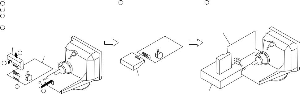
SECTION 1 DISASSEMBLY
1-1. CABINET REMOVAL
 Push in the tip of a screwdriver about 10mm to unlock the claw.
Cabinet |
Cabinet |
Bezel assembly |
Bezel assembly |
2 |
Two claws |
|
5Three screws (+BVTT 4 x 8)
A
7 EMI shield
4 Three screws (+BVTT 4 x 8)
3Push the upper side of the cabinet
in the direction of arrow A, disconnect claws,
then remove the cabinet
lifting it up in the direction of arrow B.
B
1Two screws (+BVTP 4 x 16)
EMI shield
C
6Slide the EMI shield in the direction of arrow C and remove four claws.
21T3(E) 1-1
1-2. A1 BOARD (C BLOCK) REMOVAL
1 A1 board (C BLOCK)
CN318
GND GND
CN315
21T3(E) 1-2
1-3. A1 BOARD REMOVAL
7 Video case
6 Screw (+BVTP 3 X 8)
8 A1 board
3 Four screws
(+BVTP 3 x 8)
5 Four screws (HEX)
4 Video shield
CN315
1Two screws (+BVTP 3 x 8)
2 Video block assembly
21T3(E) 1-3
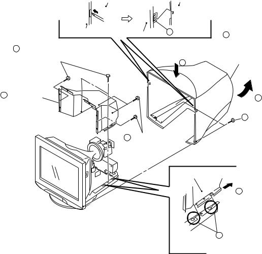
1-4. BEZEL ASSEMBLY, H3 BOARD REMOVAL
1Before removing the bezel assembly, secure the picture tube by attaching two screws to the picture tube shield at the positions shown with an arrow (diagonal two places) to prevent the picture tube from falling.
(Use the screws +BVTT 4 x 8 that fix EMI shield.)
2 Four tapping screws (5)
Picture tube shield
3 Screw
(+BVTP 4 x 16) |
|
|
|
10 L1 blacket |
|
|
|
11 Magnetic CN1500 |
4 |
Screw |
|
MIU-221D sensor |
|||
|
|
(+BVTP 4 x 16)
CN1401
CN1400
5 Bezel assembly |
9 Two claws |
6 |
Three screws |
7 Input button |
(+BVTP 3 x 10) |
8 |
H3 board |
21T3(E) 1-4
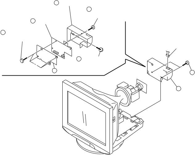
1-5. D BOARD REMOVAL
4 Two screws (+BVTP 3 x 10)
5 Rear plate assembly
6 Five screws
(+BVTP 3 x 10)
1 A1 board |
|
CN1601 |
|
(C block) |
|
CN1600 |
|
Connector (4P) |
CN1103 |
|
|
|
CN1003 |
CN605 |
CN501 |
|
|
CN701 |
|
3 Video block assembly
CN315
2Two screws
(+BVTP 3 x 8)
GND
8 D board
 7 Screw (+BVTP 3X10)
CN602
Connector (4P)
CN601
GND
21T3(E) 1-5
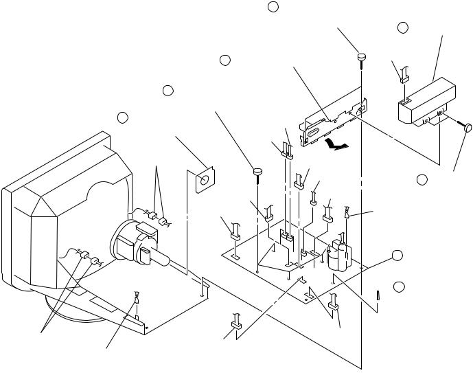
1-6. SERVICE POSITION
1Remove the D board.
2Remove the Video block assembly.
3Install the Adaptor board
(XT MOUNT) (A-1391-123-A).
4Lay the Video block assembly.
Video block assembly
2 |
D board |
|
4
3
1
5 Install the video block assembly. |
6 Put a box which is about 15cm in height |
|
under the D board to fix it. |
|
(Please disconnect the CN 701 first.) |
|
D board |
Video block assembly
Box
21T3(E) 1-6
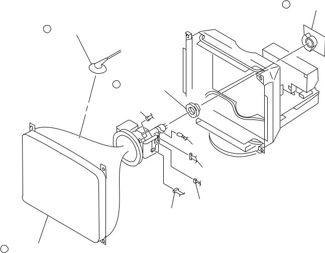
1-7. PICTURE TUBE REMOVAL
2 A1 board (C block)
1 Anode cap (Refer to 1-8)
3 Neck assembly
CN2
GND
CN3
CN2
CN1
4 Picture tube
21T3(E) 1-7
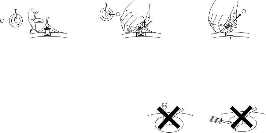
• REMOVAL OF ANODE-CAP
NOTE: Short circuit the anode of the picture tube and the anode cap to the metal chassis, CRT shield or carbon painted on the CRT, after removing the anode.
• REMOVING PROCEDURES
a
1Turn up one side of the rubber cap in the direction indicated by the arrow a.
b
2Using a thumb pull up the rubber cap
firmly in the direction indicated by the arrow b.
c
Anode Button
3When one side of the rubber cap is separated from the anode button, the anode-cap can be removed by turning up
the rubber cap and pulling up it in the direction of the arrow c.
• HOW TO HANDLE AN ANODE-CAP
1Don’t scratch the surface of anode-caps with sharp shaped material!
2Don’t press the rubber hardly not to damage inside of anodecaps!
A material fitting called as shatter-hook terminal is built in the rubber.
3Don’t turn the foot of rubber over hardly!
The shatter-hook terminal will stick out or damage the rubber.
21T3(E) 1-8
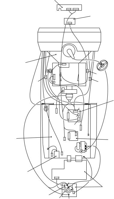
1-8. HARNESS LOCATION
H3 board
CN1401 CN1400
Magnetic sensor
CN1500
Picture tube
CN2
5P
CN1
4P |
CN3 |
4P |
CN1
D board
CN602
|
CN1602 |
|
CN701 |
|
|
CN1600 |
|
|
CN1601 |
|
|
|
|
CN501 |
|
CN1003 |
CN904 |
CN1103 |
|
|
CN604 |
CN1102 |
|
CN601 |
|
|
CN312 |
CN311 |
|
L2 board
N board
AC inlet (3P)
CN315
CN303 |
CN316 |
CN320
A1 board
CN318
CN319
21T3(E) 1-9
SECTION 2
SAFETY RELATED ADJUSTMENT
When replacing or repairing the shown below table, the
following operational checks must be performed as a
safety precaution against X-rays emissions from the unit.
|
Part Replaced ([) |
|
HV ADJ |
|
RV901 |
|
|
Part Replaced (]) |
HV Regulator |
D Board |
C925, IC901, R901, |
Circuit Check |
|
R902, R905, R924, |
|
|
R925, R926, RV901, |
|
|
T901 (FBT) |
|
|
• Mounted D Board |
HV Protector |
D Board |
C920, C923, D911, |
Circuit Check |
|
D912, R903, R917, |
|
|
R918, R919, R920, |
|
|
R923, T901 (FBT) |
|
|
• Mounted D Board |
|
N Board |
IC1001, RB1001 |
|
|
• Mounted N Board |
|
|
Part Replaced (]) |
|
|
|
Beam Current |
D Board |
C930, D917, R921, |
Protector Circuit |
|
R932, R933, R935, |
Check |
|
T901 (FBT) |
|
|
• Mounted D Board |
|
N Board |
IC1001, RB1001 |
|
|
• Mounted N Board |
|
|
|
*Confirm one minute after turning on the power.
a)HV Regulator Circuit Check
1)Turn the RV901 slowly, and adjustment so that high
voltage is in the specified range. [Specification]: 27.00 ± 0.05 kV
2)Check that the voltage of D912 cathode on the D board is 17.0 V or more.
b)HV Protector Circuit Check
1)Using external DC Power Supply, apply the voltage shown below between cathode of D912 and GND, and check that the RASTER disappers.
[Specification]: 19.95 + 0.00/–0.05 V
21T3 (E) 2-1
c)Beam Current Protector Circuit Check
1)Connect constant current source to a section between T901 (FBT) qa pin and GND, and check that the RASTER disappers when the specified current flows to the qa pin.
[Specification]: 2.12 + 0.00/–0.01 mA
21T3 (E) 2-2

SECTION 3
ADJUSTMENTS
Note: Hand degauss must be used on stand-by or power-off condition.
This model has an automatic earth magnetism correction function by using an earth magnetism sensor and a LCC coil. When using a hand degauss while monitor (LCC coil) is being operated, it sometimes gets magnetized, and the system may not work properly as a result.
• Landing Rough Adjustment
1.Display all white pattern (or black dot pattern).
2.Set contrast to 255.
3.Display green plain pattern.
4.Side back DY and roughly adjust green plain pattern to be centered on the useful screen with Purity Magnet.
5.Adjust DY tilt.
Note: Set ROTATION to 128 and LCC_NS to 128 when adjusting DY tilt. 6. LIghtly tighten the DY screw.
• Landing Fine Adjustment
Note: (1) After adjust W/B (9300k), measure the average of ∑ IK with all white video input, while CONTRAST is maximum and BRIGHTNESS is center. And adjustment shall be made so that the miss-landing become least after aging 2H with the IK 30% of measured value shown above.
(2)The magnetic field shall be BH = 0.
(3)When adjusting at other than BH = 0, calculate the shifted value from BH = 0.
1.Put the monitor in helmholz coil.
2.Set as follows;
LCC_SW = 0 (LCC Correction Current = 0) FUNCTION_SW bit1 = (Auto Degauss = On) CONTRAST = 255
3.Display green plain pattern.
4.Degauss the iron part of chassis with a hand degausser and degauss coil.
5.Degauss CRT face with a hand degausser again.
6.Input AC 230V to AC IN and turn the monitor off and on. Then autodegauss works.
7.Reset FUNCTION_SW bit1 to 0 (auto-degauss = off)
8.Degauss CRT face with a hand degausser again.
9.Attach wobbling coil to the specified place on CRT neck.
10.Put on landing sensor to CRT face.
11.Set LCC_SW to 12.
12.With landing checker, adjust DY position, purity, DY center and landing of the 4 corners.
13.Read VX and VY value which are the read out of magnetic sensor, and write to "LCC_VX_REF" and "LCC_VY_REF".
21T3 (E) 3-1

14.Adjust landing by LCC_NS, LCC_LT, LCC_LB, LCC_RT, and LCC_RB. Adjustment of registers shall be limited within the following
range.
LCC_NS: 128 ± 15
LCC_LT, LCC_LB, LCC_RT, and LCC_RB: 128 ± 40
Set LCC_SW to 13, and Perform Service Save.
<Specifications>
Adjust so that the green is within the specification given right.
4 corner adjust target : within ± 1
The red and blue must be within the specification given right with respect to the green.
A difference between red and blue must be within the specification given right.
|
|
|
|
|
( m) |
||
0 ± |
|
0 ± |
|
0 ± |
|
|
|
3 |
7.5 |
3 |
|
|
|||
|
|
||||||
0 ± |
3 |
0 ± |
7.5 |
0 ± |
3 |
|
|
0 ± |
3 |
0 ± |
7.5 |
0 ± |
3 |
|
|
|
|
|
|
|
|
|
|
|
|
|
|
|
( m) |
||
± |
6 |
± |
6 |
± |
|
6 |
|
|
|
|
|||||||
± |
6 |
± |
6 |
± |
6 |
|
|
|
± |
6 |
± |
6 |
± |
6 |
|
|
|
|
|
|
|
|
|
|
|
|
|
|
|
|
|
( m) |
|||
10 |
|
10 |
|
10 |
|
|
||
|
|
|
|
|||||
10 |
|
7 |
|
|
10 |
|
|
|
10 |
|
10 |
|
10 |
|
|
||
|
|
|
|
|
|
|
|
|
15.Tighten DY screw within specified torque, and auto-degauss. Note: Torque 22 ± 2 kgcm (2.2 ± 0.2Nm)
16.Adjust the vertical angle of DY to make top and bottom pins equal (a = b). The horizontal angle shall not be changed (straight). Settle DY upright without leaning, and insert wedges firmly so that DY shall not move.
<How to place wedge>
Green plain crosshatch pattern
|
|
a |
|
|
a and b should be equal. |
|
|
|
|
||||
|
|
|
|
|
|
|
|
|
|
|
|
|
|
|
|
|
|
|
|
|
c |
|
d |
||||
|
c and d should be equal. |
|||||
|
|
|
|
|
|
|
b
Plaster RTV to both sides for the upper wedge. Make sure that they settle inside DY.
Plaster RTV to one side for other wedges.
17.Adjust top and bottom pins correction VR.
18.Adjust the horizontal trapezoid distortion by DY horizontal trapezoid correction VR.
19.Check landing at each corner and in case not in specification, adjust landing of 4 corners with "LCC_NS", "LCC_LT", "LCC_LB", "LCC_RT", and "LCC_RB". The limitations of registers are shown
below.
LCC_NS: 128 ± 15
LCC_LT, LCC_LB, LCC_RT, and LCC_RB: 128 ± 40
20.Remove the sensor and wobbling coil.
21.Switch signals to R, G, and B, and then check that the pure colors have good color purity.
22.Fix purity magnets with white paint.
21T3 (E) 3-2
Connect the communication cable of the computer to the connector located on the D board. Run the service software and then follow the instruction.
1 1-690-391-21 2 |
A-1500-819-A |
3 3-702-691-01 |
|
|
|
Interface Unit |
Connector Attachment |
IBM AT Computer |
|
|
To BUS CONNECTOR |
as a Jig |
|
|
|
|
|
|
|
D-sub |
mini Din |
4 Pin |
4 Pin 4 Pin |
(9 Pin [female]) |
(8Pin) |
|
|
*The parts above ( 1  3 ) are necessary for DAS adjustment.
• Convergence Rough Adjustment
(1)Display white crosshatch pattern.
(2)Pile the convex parts of 6-pole magnet for convergence together.
(3)Roughly adjust H.CONV and V.CONV with 4-pole magnet.
Purity
4-pole magnet
6-pole magnet
2-pole magnet
H.TRAP
TB-PIN
XCV
TLH
XCV |
|
|
XBV |
|
|
|
TLH |
|
|
|
|
|
|||||
|
|
|
|
|
B |
|
|
|
R |
|
|
|
|
|
|
|
|
|
|
|
|
|
|
|
|
|
|
|
|
|
|
|
|
||
|
|
|
|
|
|
|
|
|
|
|
|
|
|
|
|
||
|
|
|
|
|
R |
|
|
|
B |
|
|
|
|
|
|
|
|
|
|
|
|
|
|
|
|
|
|
|
R |
|
B |
B |
|
R |
|
|
|
|
|
|
|
|
|
|
|
|
|
|
|
||||
|
|
|
|
|
|
|
|
|
|
|
|
|
|
||||
|
|
|
|
|
|
|
|
|
|
|
|
|
|
|
|
||
TLV |
|
|
YCH |
|
|
YBH |
|
|
|
|
|
||||||
|
|
|
|
|
|
|
|
|
|
|
|
|
|
|
|
|
|
|
|
|
|
|
R |
|
|
|
|
|
|
|
|
|
|
|
|
|
|
|
|
|
|
|
|
|
|
|
|
|
|
|
|
|
|
|
|
|
|
|
B |
|
|
|
|
|
|
|
|
|
|
|
|
|
|
|
|
|
B |
|
|
|
|
|
|
|
|
|
|
|
|
|
|
|
|
|
R |
|
|
R |
B |
|
|
|
R |
B |
|||
|
|
|
|
|
|
|
|
|
|
||||||||
|
|
|
|
|
|
|
|
|
|
||||||||
|
|
|
|
|
|
|
|
|
|
|
|
|
|
|
|||
• Convergence Specification |
|
|
|
|
|
|
|
|
|
||||||||
|
|
|
|
|
|
B |
|
|
|
|
|
|
|
|
|
||
|
|
|
|
|
|
|
|
|
|
|
|
|
|
|
|||
|
|
|
|
|
A |
|
|
|
|
|
|
|
|
|
|
|
|
|
V |
|
|
|
|
|
|
|
|
|
|
|
|
|
|||
|
|
|
A |
0.20 mm |
|
|
|
|
|
|
|
||||||
|
|
|
|
|
|
|
|
|
|
|
|
|
|
|
|||
|
|
|
|
|
|
|
|
|
|
|
|||||||
|
|
|
|
|
|
|
|
|
|
|
|
|
|
|
|
|
|
|
|
|
|
|
|
|
|
B |
0.24 mm |
|
|
|
|
|
|
|
|
|
|
|
|
|
|
|
|
|
|
|
|
|
|
|
|
|
|
21T3 (E) 3-3
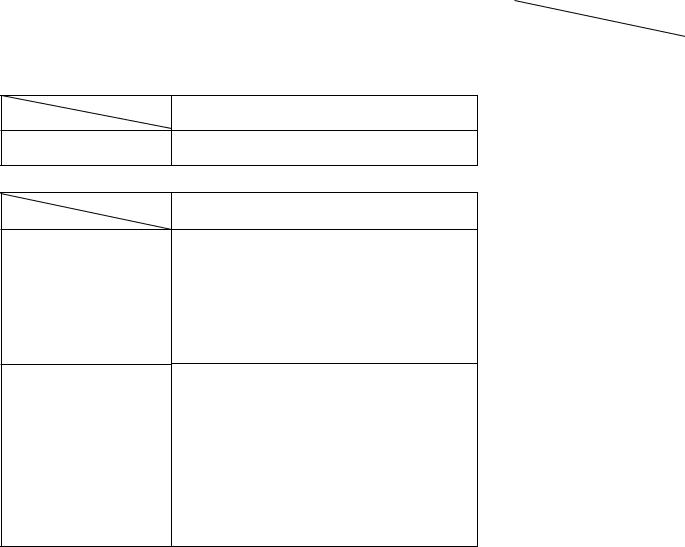
• White Balance Adjustment Specification
1.9300 K
x= 0.283 ± 0.005
y= 0.298 ± 0.005 (All White)
2.6500 K
x= 0.313 ± 0.005
y= 0.329 ± 0.005 (All White)
3.5000 K
x= 0.346 ± 0.005
y= 0.359 ± 0.005 (All White)
•Vertical and Horizontal Position and Size Specification
A |
|
|
|
|
b |
|
|
|
|
b |
|
MODE |
4 : 3 |
|
B |
|
|
||
|
A |
388 |
||
a |
a |
|||
B |
291 |
|||
|
|
|||
a |
1.8 mm |
|
|
|
b |
1.8 mm |
|
|
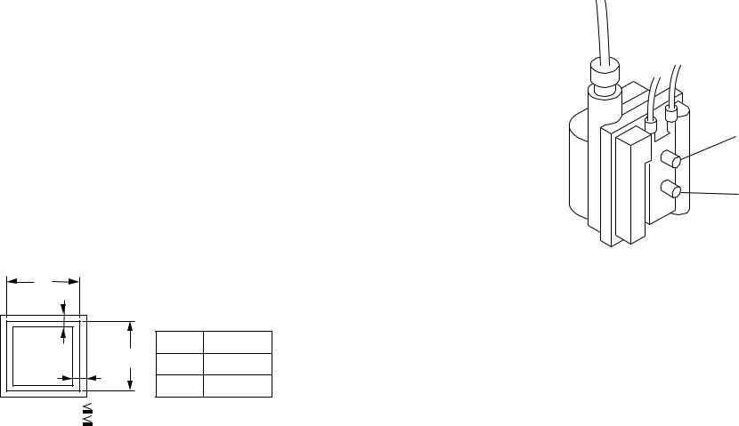
•Focus adjustment
Adjust the focus volume 1 and 2 for the optimum focus.
Focus 1
Focus 2
FBT
21T3 (E) 3-4
|
|
|
SECTION 4 |
|
|
|
|
|
|
|
|
|
|
|
|
|
|
|
|
|
|
|
|
|
|
|
|
|
|
|
|
|
|
|
|
|
|
|
|||
|
|
|
DIAGRAMS |
|
|
|
|
|
|
|
|
|
|
|
|
|
|
|
|
|
|
|
|
|
|
|
|
|
|
|
|
|
|
|
|
|
|
|
|||
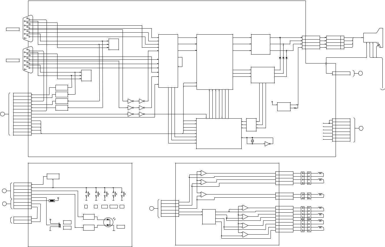
4-1. BLOCK DIAGRAMS |
|
|
|
|
|
|
|
|
|
|
|
|
|
|
|
|
|
|
|
|
|
|
|
|
|
|
|
|
|
|
|
|
|
|
|
|
|
|
|||
|
CN309 |
|
|
|
|
|
|
|
|
|
|
|
|
|
|
|
|
|
|
|
|
|
|
|
|
|
|
|
|
|
|
|
|
|
|
|
|
|
|
|
|
|
HD15 |
|
|
|
|
|
|
|
|
|
|
|
|
|
|
|
|
|
|
|
|
|
|
|
|
|
|
|
|
|
|
|
|
|
|
|
|
|
|
|
|
|
15 |
10 |
5 |
|
|
|
|
|
|
|
|
|
|
|
|
|
|
|
|
|
|
|
|
|
|
|
|
|
|
|
|
|
|
|
|
|
|
|
|
|
|
|
|
|
|
|
|
|
|
|
|
|
|
|
|
|
|
|
|
|
|
|
|
|
|
|
|
|
|
|
|
|
|
|
|
|
|
|
|
|
|
||
|
14 |
9 |
4 |
|
|
|
|
|
|
|
|
|
|
|
|
|
|
|
|
|
|
|
|
|
|
|
|
|
|
|
|
|
|
|
|
|
|
|
|
|
|
|
13 |
8 |
3 |
|
|
|
|
|
|
|
|
|
|
|
|
|
|
|
|
|
|
|
|
|
|
|
|
|
|
|
|
|
|
|
|
|
|
|
|
|
|
|
|
|
|
|
|
|
|
|
|
|
|
|
|
|
|
|
|
|
|
|
|
|
|
|
|
|
|
|
|
|
|
|
|
|
|
|
|
|
|
||
INPUT2(HD15) |
|
2 |
|
|
|
|
|
|
|
IC008 |
|
|
|
|
|
|
|
|
IC001 |
|
|
|
|
|
|
IC002 |
|
|
|
|
|
|
|
|
|
|
|||||
|
12 |
|
|
|
|
|
|
|
|
|
|
|
|
|
|
|
|
|
|
|
|
|
|
|
|
|
|
|
|
|
|
|
|
||||||||
|
7 |
|
|
|
|
|
|
|
INPUT SELECT |
|
|
|
|
|
|
RGB PRE-AMP |
|
|
|
|
|
RGB AMP |
|
|
|
|
|
|
|
|
|
||||||||||
|
|
|
|
|
|
|
|
|
|
|
|
|
|
|
|
|
|
|
|
|
|
|
CN315 |
CN318 |
|
|
|
||||||||||||||
|
|
|
1 |
|
|
|
|
|
|
|
|
|
|
|
|
|
|
|
|
|
|
|
|
|
|
|
|
|
|
|
|
|
|
|
|
|
|
|
|||
|
11 |
6 |
|
|
|
|
|
|
|
2 |
|
|
|
25 |
7 |
|
|
|
|
|
|
|
|
|
|
26 |
|
|
8 |
|
|
5 |
|
|
|
|
|
|
V901 |
||
|
|
|
|
|
|
|
|
|
|
R OUT |
|
|
|
|
|
|
|
|
|
R OUT |
|
|
|
R OUT |
|
5 |
KR |
KR |
5 |
|
|||||||||||
|
|
|
|
|
|
5 |
|
|
|
|
B1 |
|
|
R IN |
|
|
|
|
|
|
|
|
|
|
|
|
R IN |
|
|
|
PICTURE TUBE |
||||||||||
|
|
|
|
|
|
|
|
|
|
4 |
|
|
|
|
|
|
|
|
|
|
|
|
|
|
|
|
|
|
|
|
|
|
|
|
|
|
|
||||
|
|
|
|
|
|
6 |
SDA |
|
|
|
G1 |
|
|
|
28 |
4 |
|
|
|
|
|
|
|
|
|
|
28 |
|
|
9 |
|
|
3 |
|
3 |
KG |
KG |
3 |
|
|
|
|
|
|
|
|
|
|
|
|
|
6 |
|
|
|
|
|
|
|
|
|
|
|
|
|
|
|
|
|
|
|
|
|
|
|
|
|
||||||
|
CN307 |
|
|
|
|
7 |
SCL |
|
|
|
R1 |
|
G OUT |
|
G IN |
|
|
|
|
|
|
|
|
G OUT |
|
|
|
G IN |
|
G OUT |
|
|
1 |
KB |
KB |
1 |
|
|
|
||
|
HD15 |
|
|
|
|
|
|
|
|
7 |
|
|
|
|
|
|
|
|
|
|
|
|
|
|
|
|
|
|
|
|
|
|
|
|
|
|
|
|
|
|
|
|
|
|
|
|
|
VCLK |
|
|
|
V1 |
|
|
|
|
|
|
|
|
|
|
|
|
|
|
|
|
|
|
|
|
|
|
|
7 |
HEATER+ |
HEATER+ |
7 |
|
|
|
|
|
|
|
5 |
|
|
|
|
|
|
|
|
|
31 |
2 |
|
|
|
|
|
|
|
|
|
|
30 |
|
11 |
|
|
1 |
|
|
|
|
|||||||
|
15 |
|
|
|
|
|
|
|
|
8 |
|
|
|
|
|
|
|
|
|
|
|
|
|
|
|
|
|
|
|
|
|
|
|
|
|||||||
|
10 |
|
|
|
|
IC009 |
|
|
|
H1 |
|
B OUT |
|
B IN |
|
|
|
|
|
|
|
|
|
B OUT |
|
|
|
B IN |
|
B OUT |
|
|
|
|
|
|
|
|
|
||
|
|
|
|
|
|
|
|
|
|
|
|
|
|
|
|
|
|
|
|
|
|
|
|
|
|
|
|
|
|
|
|
|
|
|
|
|
|
|
|
|
|
|
14 |
9 |
4 |
|
|
|
ROM |
|
|
|
|
|
|
|
23 |
|
|
|
|
|
|
|
|
|
|
|
|
|
|
|
|
|
|
|
|
|
|
|
FV |
FC |
HV |
|
|
|
|
|
|
|
|
|
|
SOG |
|
|
|
|
|
|
|
|
|
|
|
|
|
|
|
|
|
|
|
|
|
|
|
||||||||
|
13 |
|
3 |
|
|
|
|
|
|
|
10 |
|
|
|
|
|
|
|
|
|
|
|
|
|
|
|
|
|
|
|
|
|
|
|
|
|
|
|
|
||
|
8 |
|
|
|
|
|
|
|
|
|
|
|
|
|
|
|
|
|
|
|
|
|
|
|
|
|
|
|
|
|
|
|
|
|
|
|
|
|
|||
|
|
|
|
|
|
|
|
|
B2 |
|
|
|
|
|
|
|
|
|
|
|
|
|
|
|
|
|
|
|
|
|
|
|
|
|
|
|
|
|
|
||
INPUT1(HD15) |
|
|
|
|
|
|
|
|
|
12 |
|
|
|
|
|
|
|
|
|
|
|
|
|
|
|
|
|
|
|
IC004 |
|
|
|
|
|
|
|
|
|
||
|
12 |
7 |
2 |
|
|
|
|
|
|
|
|
|
|
|
|
|
|
|
|
|
|
|
|
|
|
|
|
|
|
|
|
|
|
|
|
|
|
|
|||
|
|
|
|
|
|
|
|
|
G2 |
|
|
|
22 |
|
|
|
|
|
|
|
|
|
|
|
|
|
|
CUT OFF AMP |
|
|
|
|
G2 |
|
|
|
|
||||
|
|
|
1 |
|
|
|
|
|
|
|
|
SYNC IN |
|
|
|
|
|
|
|
|
|
|
|
|
|
|
|
|
|
|
|
|
|
|
|||||||
|
11 |
6 |
|
|
|
|
|
|
|
R2 |
|
|
|
|
|
|
|
|
|
|
|
|
22 |
|
15 |
|
|
|
3 |
|
|
|
|
|
|
|
|||||
|
|
|
|
|
|
|
|
|
|
14 |
|
|
|
|
|
|
|
|
|
|
|
|
|
|
|
|
|
|
|
|
|
|
|
|
|
|
|
|
|
|
|
|
|
|
|
5 |
|
|
|
|
|
|
15 |
|
|
|
|
|
|
|
|
|
|
|
|
|
|
COF R |
|
|
|
RIN |
|
ROUT |
|
|
|
|
CN318 |
|
|
|
|
|
|
|
|
|
|
|
|
|
|
|
|
|
|
|
|
|
|
|
|
|
|
|
|
|
23 |
|
14 |
|
|
|
5 |
|
|
|
|
|
|
|
|
||
|
|
|
|
SDA |
|
|
|
|
|
|
V2 |
|
|
|
|
|
|
|
|
|
|
|
|
|
|
COF G |
|
GIN |
|
|
|
|
|
1 |
G2 |
B |
|
|
|||
|
|
|
|
6 |
|
|
|
|
|
|
|
|
|
|
|
|
|
|
|
|
|
|
|
|
|
|
|
|
|
GOUT |
|
|
|
|
|
||||||
|
|
|
|
SCL |
|
|
|
|
|
|
16 |
|
|
|
|
|
|
|
|
|
|
|
|
|
|
COF B |
24 |
|
13 |
BIN |
|
|
7 |
|
|
|
|
|
|
|
|
|
|
|
|
7 |
|
|
|
|
|
|
H2 |
|
|
|
|
|
|
|
|
|
|
|
|
|
|
|
|
|
|
BOUT |
|
|
|
|
|
|
|
|
|||
|
|
|
|
VCLK |
|
|
|
|
|
|
|
|
|
G.SYNC |
|
|
|
|
|
|
|
|
|
|
|
|
|
|
|
R IK |
G IK |
B IK |
|
|
|
|
|
|
|
|
|
|
|
|
|
IC007 |
|
|
|
|
|
|
13 |
OUTH |
OUTV |
SCL |
22 |
|
|
|
ROSD |
GOSD |
BOSD |
BLKOSD |
DETV |
BLK |
CLAMP |
|
|
|
|
|
|
|
|
|
|
|
|
||||
|
|
|
|
|
|
|
|
|
|
|
|
|
|
|
|
|
|
|
|
|
|
|
|
|
|
|
|
||||||||||||||
|
|
|
|
|
|
|
|
|
|
|
|
|
|
SCL |
|
|
|
|
|
|
|
|
|
|
|
|
|
|
|
|
|
|
|
|
|
|
|
|
|
||
|
|
|
SW |
ROM |
|
|
|
|
|
|
SW |
|
|
|
SDA |
23 |
|
|
|
|
|
|
|
|
|
|
|
|
|
12 |
11 |
10 |
|
|
|
|
|
|
|
|
|
|
|
|
|
|
|
|
|
|
|
|
|
|
|
|
SDA |
|
|
|
|
|
|
|
|
|
|
|
|
|
|
|
|
|
|
|
|
|
|
|
|
|
|
|
CN311 |
|
Q004 |
|
|
|
|
|
|
|
18 |
19 |
21 |
|
|
|
|
|
|
|
|
|
|
|
|
|
|
|
|
|
|
|
|
|
|
|
|
|
|
|
|
|
|
|
|
|
|
|
|
|
|
|
|
|
|
|
|
|
|
|
|
|
|
|
|
|
|
|
|
|
|
|
|
|
|
|
|
|
|
||||
|
|
|
|
|
|
|
|
IC006 |
|
|
|
|
|
|
|
|
15 |
|
14 |
13 |
12 |
10 |
17 |
18 |
|
|
|
|
|
|
|
|
|
|
|
|
|
|
TO D BOARD |
||
|
|
|
SW |
|
|
|
|
|
|
|
|
|
|
|
|
|
|
|
|
|
|
|
|
|
|
|
|
|
|
|
|
||||||||||
|
DDC SCL1 |
10 |
|
|
|
|
|
|
|
|
|
|
|
|
|
|
|
|
|
|
|
|
|
|
|
|
|
|
|
|
|
|
|
|
|
|
|
||||
|
Q005 |
|
|
|
|
|
INVERTER |
|
|
|
|
|
|
|
|
|
|
|
|
|
|
|
|
|
|
|
|
|
|
|
|
|
|
|
|
|
|
FBT |
|||
|
DDC SDA1 |
11 |
SW |
|
|
|
|
9 |
8 |
5 |
6 |
|
|
|
|
|
|
|
|
|
|
|
|
|
|
|
|
|
|
|
|
|
7V |
IC011 |
|
|
|
|
|
|
|
|
DDC GND1 |
9 |
|
|
|
|
|
|
|
|
|
|
|
|
|
|
|
|
|
|
|
|
|
|
|
|
|
HEATER REG |
|
|
|
|
|
|
|||||||
|
Q002 |
|
|
|
|
|
|
|
|
|
|
|
|
|
|
|
|
|
|
|
|
|
|
|
|
|
|
|
|
|
|
|
|
|
|
|
|
||||
|
|
|
|
|
|
|
|
|
|
|
|
|
|
|
|
|
|
|
|
|
|
|
|
|
|
|
|
|
|
|
|
|
|
|
|
|
|
|
|||
|
|
|
|
|
|
|
|
|
|
|
|
|
|
|
|
|
|
|
|
|
|
|
|
|
|
|
|
|
|
|
|
2 |
|
4 |
|
|
|
|
|
|
|
|
DDC SCL2 |
7 |
|
|
|
|
|
|
|
|
|
|
|
|
|
|
|
|
|
|
|
|
|
|
|
|
|
|
|
|
|
|
Vcc |
|
|
|
|
|
|
||
|
SW |
|
|
|
|
3 |
4 |
11 |
10 |
|
|
|
|
|
|
|
|
|
|
|
|
|
|
|
|
|
|
|
|
|
|
OUT |
|
|
|
|
|
|
|||
|
DDC SDA2 |
8 |
|
|
|
|
|
|
|
|
|
|
|
|
|
|
|
|
|
|
|
|
|
|
|
|
|
|
|
5 |
|
|
|
|
|
|
|||||
|
Q001 |
|
|
|
|
|
|
|
|
|
|
|
|
|
|
|
|
|
|
|
|
|
|
|
|
|
|
|
|
|
|
|
VADJ |
|
|
|
|
|
|
||
|
DDC GND2 |
6 |
|
|
|
|
|
|
|
|
|
|
|
|
|
|
|
|
|
|
|
|
|
|
|
|
|
|
|
|
|
|
|
|
|
|
|
|
|
|
|
|
|
|
|
|
|
1 |
2 |
13 |
12 |
|
|
|
|
|
|
|
|
|
|
|
|
|
|
|
|
|
|
|
|
|
|
|
|
|
|
|
|
|
|
||
A |
H BLK |
1 |
|
|
|
|
|
|
|
|
|
|
|
|
|
|
|
|
|
|
|
|
|
|
|
|
|
|
|
|
|
|
|
|
|
|
|
||||
|
|
|
|
|
|
|
|
|
|
|
|
|
|
2 |
|
18 |
|
20 |
19 |
21 |
7 |
11 |
10 |
|
|
|
|
|
|
|
|
|
|
|
CN312 |
|
|
|
|||
TO D BOARD |
INPUT SW |
4 |
|
|
|
|
|
|
|
|
|
|
|
|
|
|
|
|
|
|
|
|
|
|
|
|
|
|
|
|
|
|
|||||||||
SCL |
|
|
|
|
|
|
|
|
|
|
|
SCL |
4 |
|
|
|
|
|
|
|
|
|
|
|
|
|
|
|
|
|
|
|
|
|
|
|
|
|
|||
|
|
|
|
|
|
|
|
|
|
|
|
|
|
HFLY |
OSDR |
OSDG |
OSDB |
OSDBLK |
AV |
BLK |
CLP |
|
32 |
|
|
|
|
|
|
|
|
1 |
+B |
|
|
|
|||||
CN1102 |
IIC SCL |
15 |
HS OUT |
|
|
|
|
|
|
|
|
|
|
|
HS OUT |
12 |
|
GCI |
|
Q201, |
|
|
|
|
|
|
|
|
|
||||||||||||
|
|
|
SDA |
|
|
|
|
|
|
|
|
|
|
|
SDA |
3 |
|
|
|
|
|
|
|
|
|
|
RCI |
31 |
BUFFER |
|
|
|
|
|
+B |
|
+B |
|
|
|
|
|
IIC SDA |
16 |
|
|
|
|
|
|
|
|
|
|
|
|
|
SDA |
|
|
|
|
|
|
|
|
|
|
|
|
Q101, |
|
|
|
|
|
2 |
|
|
|
|||
|
HS OUT |
2 |
VS OUT |
|
|
|
|
|
|
|
|
|
|
|
VS OUT |
HS OUT |
|
|
|
|
|
|
|
|
|
BCI |
30 |
|
Q301 |
|
|
|
|
|
+80V |
4 |
+80V |
C |
|
|
|
|
VS OUT |
3 |
|
|
|
|
|
|
|
|
|
|
|
13 |
|
|
|
|
|
|
|
|
|
|
|
|
|
|
|
|
|
+12V |
6 |
+12V |
|
|
|||||
|
|
|
|
|
|
|
|
|
|
|
|
|
|
VS OUT |
|
|
|
|
|
|
|
|
|
|
|
|
|
|
|
|
|
|
|
|
|
||||||
|
ECO SW |
13 |
ECO SW |
|
|
|
|
|
|
|
|
|
|
|
ECO SW 27 |
|
|
|
|
|
|
|
|
|
|
|
|
|
|
|
|
|
|
|
7V |
7 |
7V |
TO D BOARD |
|
|
|
|
|
|
|
|
|
|
|
|
|
|
|
|
|
ECO SW |
|
|
|
|
|
IC003 |
|
|
|
|
|
|
|
|
|
|
|
|
|
||||||||
|
|
|
|
|
|
|
|
|
|
|
|
|
|
|
|
23 |
|
|
|
|
|
|
|
|
|
14 |
|
|
|
|
|
|
|
3.3V |
8 |
3.3V |
CN604 |
|
|
||
|
|
|
|
|
|
|
|
|
|
|
|
|
|
|
|
CS IN |
|
|
|
|
|
OSD |
|
|
XTAL IN |
|
|
|
|
|
|
|
|
|
|
||||||
|
|
|
|
|
|
|
|
|
|
|
|
|
|
|
|
24 |
|
|
|
|
|
|
|
|
|
|
|
|
|
X001 |
|
|
|
|
|
5V |
9 |
5V |
|
|
|
|
|
|
|
|
|
|
|
|
|
|
|
|
|
|
|
VS IN |
|
|
|
|
|
|
|
|
|
|
|
|
|
|
|
|
|
|
|
|
|||||
|
|
|
|
|
|
|
|
|
|
|
|
|
|
|
|
25 |
|
|
|
|
|
|
|
|
|
|
|
|
|
24.5MHz |
2 |
4 |
|
|
|
|
|
|
|
|
|
|
|
|
|
|
|
|
|
|
|
|
|
|
|
|
|
HS IN |
|
|
|
|
|
|
|
|
|
|
|
|
|
|
|
|
|
|
|
|
|
|
|
|
|
|
|
|
A1 (VIDEO AMP, RGB OUT) |
|
|
|
|
|
|
|
|
|
|
|
|
|
|
|
|
|
|
|
|
|
|
|
|
|
|
|
|
IC005 |
|
|
|
|
|
|
|
|
|
|
|
|
|
|
|
|
|
|
|
|
|
|
|
|
|
|
|
|
|
|
|
|
|
|
|
|
|
|
|
INVERTER |
|
|
|
|
|
|
|
|
|
||
|
|
|
|
|
|
|
|
|
|
|
|
|
|
|
|
|
|
|
|
|
|
|
|
|
|
|
|
|
|
|
|
|
|
|
|
|
|
|
|
|
|
|
|
|
|
|
|
|
|
|
|
|
|
|
|
|
|
4 |
+ |
|
|
IC1600 |
|
|
|
|
|
|
|
|
|
|
|
CN1601 |
|
|
|
|
|
|
|||
|
|
|
|
|
|
|
|
|
|
|
|
|
|
|
|
3 |
|
2 |
(1/2) |
|
|
|
|
|
|
|
|
|
|
|
3 |
CY4+ |
|
|
|
|
|
|
|
||
|
|
|
|
|
|
|
|
|
|
|
|
|
|
|
|
– |
|
|
|
|
|
|
|
|
|
|
|
|
|
|
|
|
|
|
|
|
|
|
|||
|
|
|
Q1402 |
|
|
|
|
|
|
|
|
|
|
|
|
|
|
|
|
IC1600 |
|
|
|
|
|
|
|
|
|
|
4 |
CY4– |
|
|
|
|
|
|
|
||
|
|
|
|
|
|
|
|
|
|
|
|
|
|
|
6 |
|
|
|
|
|
|
|
|
|
|
|
|
|
|
|
|
|
|
|
|
|
|
||||
|
CN1400 |
|
|
|
|
|
|
|
|
|
|
|
|
|
|
+ |
|
|
|
|
|
|
|
|
|
|
|
|
1 |
CY3+ |
|
|
|
|
|
|
|
||||
|
|
|
|
|
|
|
|
|
|
|
|
|
|
|
7 |
|
8 |
(2/2) |
|
|
|
|
|
|
|
|
|
|
|
|
|
|
|
|
|
|
|||||
|
WAKE UP |
2 |
|
|
|
|
|
|
|
|
|
|
|
|
|
– |
|
|
|
|
|
|
|
|
|
|
|
|
|
|
|
2 |
CY3– |
|
|
|
|
|
|
|
|
|
|
|
|
|
|
|
|
|
|
|
|
|
|
|
|
|
|
|
|
|
|
|
|
|
|
|
|
|
|
|
|
|
|
|
|
|
|
|
|
||
|
KEY SCAN |
3 |
|
|
|
|
|
|
|
|
|
|
|
|
|
|
IC1603 |
|
|
|
|
|
|
|
|
|
|
|
|
|
|
|
|
|
|
|
|
|
|
||
D |
LED1 |
4 |
|
|
|
|
|
|
|
|
|
|
|
|
|
|
|
|
|
|
|
|
|
|
|
|
|
|
|
|
CN1600 |
|
|
|
|
|
|
||||
|
|
|
|
|
|
|
|
|
|
|
|
|
1 |
+ |
|
4 |
|
|
|
|
|
|
|
|
|
|
|
|
|
|
|
|
|
|
|
|
|||||
|
LED2 |
5 |
|
|
|
|
|
|
|
|
|
|
|
|
|
2 |
|
|
|
|
|
|
|
|
|
|
|
|
|
|
1 |
LCC-NS (+) |
|
|
|
|
|
|
|||
TO D BOARD |
5V |
|
|
|
|
|
|
|
|
|
|
|
|
– |
|
|
|
|
|
|
|
|
|
|
|
|
|
|
|
|
LCC-NS |
|
|
|
|
||||||
INPUT SW |
8 |
|
|
|
|
|
|
|
CN1603 |
|
|
|
|
|
|
|
|
|
|
|
|
|
|
|
|
|
|
|
|
|
|
||||||||||
CN1103 |
|
|
|
|
|
|
|
|
|
|
|
|
|
|
|
|
|
|
|
|
|
|
|
|
|
|
|
2 |
LCC-NS (–) |
|
|
|
|
|
|
||||||
|
T_AMB |
12 |
|
|
|
|
|
|
|
|
|
GXSC |
4 |
|
|
|
|
|
|
|
|
|
|
|
|
|
|
|
|
|
|
|
|
|
|
|
|
|
|
|
|
E |
VY |
13 |
TH1400 |
S1401 |
S1400 |
S1402 |
S1404 |
S1405 |
|
|
|
|
|
|
|
|
|
|
|
|
|
|
|
|
|
|
|
|
|
|
|
|
|
|
|
|
|
|
|||
|
|
|
GYSC |
5 |
|
|
|
|
|
|
|
|
|
|
|
|
4 |
|
|
IC1601 |
|
|
|
CN1602 |
|
|
|
|
|
|
|||||||||||
– |
+ |
BRT+ |
CONT– |
OK |
|
|
|
|
|
|
IC1602 |
|
|
|
|
|
+ |
2 |
|
|
|
|
|
|
|
|
|
||||||||||||||
|
VX |
14 |
|
|
|
|
|
|
|
|
|
|
|
|
|
(1/2) |
|
|
|
|
|
|
|
|
|
|
|
||||||||||||||
TO N BOARD |
|
|
|
F |
LCC NS |
6 |
|
|
|
|
DAC |
|
|
|
|
|
3 |
|
|
1 |
LCC-LT (+) |
|
|
|
|
|
|
||||||||||||||
|
|
|
|
|
|
|
|
|
|
|
21 |
|
|
|
2 |
|
|
|
– |
|
|
|
|
|
LCC-LT |
|
|
|
|
||||||||||||
CN1003 |
|
|
|
|
|
|
|
|
|
|
|
IIC SDA |
7 |
|
SDA |
|
AO2 |
|
|
|
|
|
|
|
|
|
2 |
LCC-LT (–) |
|
|
|
|
|
|
|||||||
|
|
|
|
|
|
|
|
|
|
|
TO D BOARD |
|
20 |
|
1 |
|
|
|
6 |
|
|
IC1601 |
|
|
|
|
|
|
|
|
|||||||||||
|
CN1401 |
|
|
|
|
|
|
|
|
|
IIC SCL |
8 |
|
SCL |
|
AO1 |
|
|
|
+ |
|
|
|
3 |
LCC-LB (+) |
|
|
|
|
|
|
||||||||||
|
|
5V |
LED DRIVE |
|
G |
|
|
|
|
CN1106 |
|
|
|
4 |
|
|
|
7 |
8 |
(2/2) |
|
|
|
LCC-LB |
|
|
|
|
|||||||||||||
TO MAGNETIC |
VX |
3 |
Q1400 |
|
|
|
|
|
|
|
|
|
|
|
|
|
|
|
AO4 |
|
|
|
– |
|
|
|
|
4 |
LCC-LB (–) |
|
|
|
|
|
|
||||||
S1403 |
|
|
|
|
|
|
|
|
|
|
|
|
|
|
|
|
|
3 |
|
|
|
|
|
|
|
|
|
5 |
LCC-RT (+) |
|
|
|
|
|
|
||||||
SENSOR UNIT |
VY |
2 |
|
|
|
|
|
|
|
|
|
|
|
|
|
|
|
|
|
AO3 |
|
|
|
|
|
|
IC1604 |
|
|
|
|
|
|
|
|
||||||
INPUT1 |
|
|
|
|
D1400 |
|
|
|
|
|
|
|
|
|
|
|
|
|
|
|
|
4 |
|
|
|
|
|
LCC-RT |
|
|
|
|
|||||||||
|
|
|
|
|
|
|
|
|
|
|
|
|
|
|
|
|
|
|
|
|
|
|
|
|
+ |
2 |
|
|
6 |
LCC-RT (–) |
|
|
|
|
|
||||||
|
|
|
|
|
|
|
|
|
|
|
|
|
|
|
|
|
|
|
|
|
|
|
|
|
|
|
(1/2) |
|
|
|
|
|
|
|
|
||||||
|
|
|
|
LED DRIVE |
|
|
|
|
|
|
|
|
|
|
|
|
|
|
|
|
|
|
|
|
|
|
3 |
|
|
|
|
|
|
|
|
||||||
|
|
|
INPUT2 |
|
A |
|
POWER |
|
|
|
|
|
|
|
|
|
|
|
|
|
|
|
|
|
|
– |
|
|
|
|
7 |
LCC-RB (+) |
|
|
|
|
|
|
|||
|
|
|
Q1401 |
|
|
|
|
|
|
|
|
|
|
|
|
|
|
|
|
|
|
|
|
|
|
|
|
|
|
|
|
LCC-RB |
|
|
|
|
|||||
|
|
|
|
|
|
|
|
|
|
|
|
|
|
|
|
|
|
|
|
|
|
|
|
|
|
|
|
|
IC1604 |
|
|
8 |
LCC-RB (–) |
|
|
|
|
|
|||
|
|
|
|
|
|
|
|
|
|
|
|
|
|
|
|
|
|
|
|
|
|
|
|
|
|
|
6 |
+ |
8 |
|
|
|
|
|
|
|
|
||||
|
|
|
|
|
|
|
|
|
|
|
|
|
|
|
|
|
|
|
|
|
|
|
|
|
|
|
7 |
(2/2) |
|
|
|
|
|
|
|
|
|
|
|
||
|
|
|
|
|
|
|
|
|
|
|
|
|
|
|
|
|
|
|
|
|
|
|
|
|
|
|
– |
|
|
|
|
|
|
|
|
|
|
|
|
|
|
|
|
|
H3 (USER CONTROL) |
|
|
|
|
|
|
|
|
|
|
|
L2 (CY, LCC) |
|
|
|
|
|
|
|
|
|
|
|
|
|
|
|
|
|
|
|
|
|
|
|
|
|
|
|
|
|
|
|
|
|
|
|
|
|
|
|
|
|
|
|
|
|
|
|
|
|
|
|
|
|
|
|
|
B-SS9342<AEP>-BD1-EPS05 |
|
|
|
|
|
|
|
||||
21T3 (E) 4-1

|
|
DA (DPU) |
|
|
|
|
|
|
|
|
|
|
|
IC1001 |
|
|
|
|
|
|
|
|
|
|
|
|
|
CN1001 |
|
|
CPU |
|
|
|
|
|
|
|
|
|
|
|
|
|
IC1101 |
|
|
|
|
|
|
|
|
|
|
|
|
|
|
|
|
|
|
|
|
22 |
|
|
|
|
|
|
CN1101 |
|
|
|
|
|
|
|
DPU |
|
LB DET |
32 |
P42/AN10 |
|
|
|
|
|
|
|
|
|
|
|
|
|
|
IK SIGMA |
34 |
21 |
|
|
|
|
|
|
H.DF |
1 |
|
|
|
|
|
1 |
HDF1 |
|
P41/AN09 |
|
|
|
|
||
|
|
|
|
|
|
|
|
DDC SDA1 |
7 |
51 |
|
|
|
|
|||
|
REFDC |
33 |
|
|
|
|
|
2 |
DCC2 |
|
P86/SDA1 |
|
|
|
|
||
|
|
|
|
|
|
|
|
DDC SCL1 |
9 |
52 |
|
|
|
|
|||
|
XDC |
37 |
|
|
|
|
|
3 |
XDC |
|
P87/SCL1 |
|
|
|
|
||
|
|
|
|
|
|
|
|
|
|
71 |
|
|
|
CN1003 |
|||
|
|
|
|
|
|
|
|
21 |
HDOUT |
|
DDC GND1 |
11 |
P21/A1/A17 |
|
|
|
|
|
HD OUT |
34 |
|
|
|
|
|
|
16 |
|
|
|
|||||
|
|
|
|
|
|
|
|
DDC SDA2 |
13 |
49 |
|
4 |
T_AMB |
||||
|
HFBP |
36 |
|
|
|
|
|
23 |
FBP-IN |
|
P84/SDA2 |
P54/AN04 |
|
||||
|
|
|
|
|
|
|
|
DDC SCL2 |
15 |
50 |
17 |
|
3 |
VY |
|||
|
H BLK |
15 |
|
|
|
|
|
35 |
H BLK |
|
P85/SCL2 |
P55/AN05 |
|
||||
|
|
|
|
|
|
|
|
DDC GND2 |
17 |
70 |
18 |
|
2 |
VX |
|||
|
VS OUT |
11 |
|
|
|
|
|
36 |
V-IN |
|
P20/A0/A16 |
P56/AN06 |
|
||||
|
|
|
|
|
|
|
|
INPUT SW |
29 |
80 |
|
|
|
|
|||
|
HS OUT |
13 |
|
|
|
|
|
38 |
H-IN |
|
P27/A7/A23 |
|
|
|
|
||
|
|
|
|
|
|
|
|
IIC SDA |
1 |
35 |
|
|
|
|
|||
|
PLL LOCK |
7 |
|
|
|
|
|
39 |
LOCK-DET |
|
P80/SDA0/SI0 |
|
|
|
|
||
|
|
|
|
|
|
|
|
IIC SCL |
3 |
36 |
|
|
|
|
|||
|
IIC SDA |
20 |
|
|
|
|
|
40 |
SDA |
|
P81/SCL0/SO0 |
|
|
|
|
||
|
|
|
|
|
|
|
|
|
|
37 |
|
IC1003 |
|
|
|||
|
|
|
|
|
|
|
|
41 |
|
|
TXD |
2 |
P82/TXD0 |
|
|
|
|
|
IIC SCL |
19 |
|
|
|
|
|
SCL |
|
|
ROM |
|
|
||||
|
|
|
|
|
|
|
|
RXD |
4 |
38 |
|
|
|
||||
|
LCC_NS |
22 |
|
|
|
|
|
43 |
LCC_NS |
|
P83/RXD0 |
64 |
7 |
|
|
||
|
|
|
|
|
|
|
|
KEY SCAN |
35 |
23 |
|
|
|||||
G |
HSAW_SW |
24 |
|
|
|
|
|
44 |
HSAW_SW |
|
P42/AN11 |
P12/A10/AD10 |
WC |
|
|
||
|
|
|
|
|
|
|
LED1 |
33 |
79 |
63 |
6 |
|
|
||||
|
H.LINBAL |
16 |
|
|
|
|
|
45 |
PWM2 |
|
P26/A6/A22 |
P11/A9/AD9 |
SCL |
|
|
||
TO D BOARD |
|
|
|
|
|
|
|
LED2 |
31 |
78 |
62 |
5 |
|
|
|||
GYSC |
21 |
|
|
|
|
|
48 |
GYSC |
|
P25/A5/A21 |
P10/A8/AD8 |
SDA |
|
|
|||
CN502 |
|
|
|
|
|
|
|
PLL LOCK |
39 |
34 |
|
|
|
|
|||
|
GXSC |
23 |
|
|
|
|
|
49 |
GXSC |
I |
P76/SCK0/INT3 |
|
|
|
|
||
|
|
|
|
|
|
|
POC |
40 |
31 |
|
|
|
|
||||
|
V.DF |
2 |
|
|
|
|
|
50 |
VDF |
|
P73/TB01N0/IN5 |
|
|
|
|
||
|
|
|
|
|
|
|
TO D BOARD |
|
|
19 |
|
|
|
|
|||
|
D.TILT |
38 |
|
|
|
|
|
51 |
VKEY |
HV DET |
6 |
P57/AN07 |
|
|
|
|
|
|
|
|
|
|
|
|
CN1104 |
ABL DET |
8 |
20 |
|
5V |
|
|
|||
|
YSC |
39 |
|
|
|
|
|
52 |
YSC |
|
P40/AN08 |
|
|
|
|||
|
|
|
|
|
|
|
|
G2 |
10 |
28 |
|
|
|
|
|||
|
XSC |
40 |
|
|
|
|
|
53 |
XSC |
|
P70/TA1OUT |
|
|
|
|
||
|
|
|
|
|
|
|
|
S6 |
12 |
7 |
|
|
|
|
|||
|
HSHAPE |
32 |
|
|
|
|
|
54 |
HSHAPE |
|
P36/TA7OUT |
46 |
I |
IC1002 |
|
||
|
|
|
|
|
|
|
|
S5 |
14 |
6 |
|
||||||
|
YDC |
35 |
|
|
|
|
|
63 |
YDC |
|
P35/TA61N |
RESET |
O |
RESET |
|
||
|
|
|
|
|
|
|
|
|
|
5 |
|
G |
|
||||
|
|
|
|
|
|
|
|
S4 |
16 |
|
|
|
|||||
|
POC |
5 |
|
|
|
|
|
27 |
POC-OUT |
|
P34 |
|
|
|
|
||
|
|
|
|
|
|
|
|
S3 |
18 |
4 |
|
|
|
|
|||
|
DCC2 |
12 |
|
|
|
|
|
26 |
POC-IN |
|
P33/MAIT |
|
|
|
|
||
|
|
|
|
|
|
|
|
S2 |
24 |
3 |
|
|
|
|
|||
|
VSAWN |
10 |
|
|
IC1102 |
|
|
64 |
DCC |
|
P32/HWR |
|
|
|
|
||
|
|
|
|
|
|
|
|
|
2 |
|
|
|
|
||||
|
|
|
|
|
AMP |
|
|
58 |
ASW1 |
|
S1 |
26 |
P31/WR |
|
|
|
|
|
|
|
|
|
|
|
|
|
|
S0 |
28 |
1 |
|
|
|
|
|
|
|
|
|
|
|
|
|
59 |
ASW2 |
|
P30/RD |
41 |
|
|
|
||
|
|
|
|
|
|
|
|
|
|
PWR SW |
23 |
58 |
|
|
|
||
|
|
|
|
3 |
7 |
+ |
5 |
61 |
VSAWL |
|
P04/AD4 |
X2 |
|
|
|
||
|
|
|
|
|
|
|
|
|
60 |
|
X1001 |
|
|
||||
|
|
2 |
+ |
|
|
– |
6 |
62 |
VSAWH |
|
DGC SW |
25 |
P06/AD6 |
|
|
|
|
|
|
|
|
|
43 |
16.9344MHz |
|
|
|||||||||
|
|
|
– |
4 |
|
|
|
|
|
|
10 |
|
|
||||
|
|
|
|
|
|
|
|
|
|
V.FBP |
30 |
P61/CTS0 |
X1 |
|
|
|
|
|
|
|
|
|
|
|
|
|
|
|
|
|
|
||||
|
|
|
|
|
|
|
|
|
|
|
WAKE UP |
36 |
13 |
|
|
|
|
|
|
|
|
|
|
|
|
|
|
|
P51/AN01 |
|
|
|
|
||
|
|
|
|
|
|
|
|
|
|
|
ECO SW |
5 |
9 |
|
|
|
|
|
|
|
|
|
|
|
|
|
|
|
P60/INT0 |
|
|
|
|
||
|
|
|
|
|
|
|
|
|
|
|
|
|
INVERTER |
|
|
|
|
|
|
|
|
|
|
|
|
|
|
|
|
|
Q1001 |
|
|
|
|
|
|
|
|
|
|
|
|
|
|
|
|
|
N ( -COM) |
|
|
|
|
|
|
|
|
|
|
|
|
|
|
|
|
|
|
|
B-SS9342<AEP>-BD2-EPS05 |
|
|
E
TO H3 BOARD CN1400
21T3 (E) 4-2

AC IN |
CN602 |
F601 |
T601 |
S601 |
|
AC L |
1 |
:LFT |
|
|
|
|
||
|
NC |
2 |
|
|
|
AC N |
3 |
|
|
DGC |
CN601 |
|
RY603 |
TH601 |
|
|
|
||
|
DGC |
1 |
|
RY602 |
|
|
|
|
|
|
DGC |
4 |
|
|
|
|
THP602 |
|
|
|
|
|
RELAY DRIVE |
|
|
|
|
Q611 |
|
|
CN1104 |
|
|
|
|
|
LB DET |
32 |
+15V |
|
|
|
IK SIGMA |
34 |
+15V |
CN1102 |
|
|
DDC SDA1 |
7 |
11 |
DDC SDA1 |
|
|
DDC SCL1 |
9 |
10 |
DDC SCL1 |
|
|
DDC GND1 |
11 |
9 |
DDC GND1 |
|
|
DDC SDA2 |
13 |
8 |
DDC SDA2 |
|
|
DDC SCL2 |
15 |
7 |
DDC SCL2 |
|
|
DDC GND2 |
17 |
6 |
DDC GND2 |
|
|
ECO SW |
5 |
13 |
ECO SW |
A |
|
INPUT SW |
29 |
4 |
INPUT SW |
TO A1 BOARD |
|
IIC SDA |
IIC SDA |
IIC SDA |
IIC SDA |
|
|
1 |
16 |
CN311 |
||
|
|
IIC SCL |
IIC SCL |
|
|
|
IIC SCL |
IIC SCL |
|
||
|
3 |
15 |
|
||
|
TXD |
TXD |
VS OUT |
VS OUT |
|
|
2 |
3 |
|
||
|
RXD |
RXD |
HS OUT |
HS OUT |
|
|
4 |
2 |
|
||
|
WAKE UP |
WAKE UP |
H BLK |
H BLK |
|
|
36 |
1 |
|
||
|
KEY SCAN |
KEY SCAN |
|
|
|
|
35 |
|
|
|
|
|
LED1 |
LED1 |
|
CN1101 |
|
I |
33 |
TXD |
|
||
LED2 |
LED2 |
TXD |
|
||
|
31 |
4 |
ECS |
||
TO N BOARD |
|
PLL LOCK |
RXD |
|
|
PLL LOCK |
39 |
3 |
RXD |
|
|
CN1001 |
POC |
POC |
|
|
|
|
40 |
|
|
|
|
|
HV DET |
HV DET |
|
CN1103 |
|
|
6 |
WAKE UP |
|
||
|
ABL DET |
ABL DET |
WAKE UP |
|
|
|
8 |
2 |
|
||
|
G2 |
G2 |
KEY SCAN |
KEY SCAN |
|
|
10 |
3 |
|
||
|
S6 |
S6 |
LED1 |
LED1 |
D |
|
12 |
4 |
|||
|
S5 |
S5 |
LED2 |
LED2 |
|
|
14 |
5 |
TO H3 BOARD |
||
|
S4 |
S4 |
8 |
INPUT SW |
|
|
16 |
CN1400 |
|||
|
S3 |
S3 |
|
|
|
|
18 |
|
|
|
|
|
S2 |
S2 |
|
CN1106 |
|
|
24 |
GXSC |
|
||
|
S1 |
S1 |
GXSC |
|
|
|
26 |
4 |
|
||
|
S0 |
S0 |
GYSC |
GYSC |
|
|
28 |
5 |
|
||
|
PWR SW |
PWR SW |
LCC NS |
LCC NS |
F |
|
23 |
6 |
|||
|
DGC SW |
DGC SW |
IIC SDA |
IIC SDA |
|
|
25 |
7 |
TO L2 BOARD |
||
|
V.FBP |
V.FBP |
IIC SCL |
IIC SCL |
|
|
30 |
8 |
CN1603 |
||
|
|
|
|
|
|
|
CN502 |
|
IIC SCL |
|
|
IIC SCL |
19 |
IIC SDA |
|
|
IIC SDA |
20 |
|
|
|
VSOUT |
||
|
|
VSOUT |
11 |
|
|
|
HSOUT |
||
|
|
HSOUT |
13 |
|
|
|
H BLK |
||
|
|
H BLK |
15 |
|
|
|
GXSC |
||
|
|
GXSC |
21 |
|
|
|
GYSC |
||
|
|
GYSC |
23 |
|
|
|
LCC NS |
||
|
|
LCC NS |
22 |
|
|
|
PLL LOCK |
||
|
|
PLL LOCK |
7 |
|
|
|
POC |
||
|
|
POC |
5 |
|
|
|
H.DF |
||
|
|
H.DF |
1 |
|
|
|
V.DF |
||
|
|
V.DF |
2 |
|
|
|
VSAWN |
||
G |
|
VSAWN |
10 |
|
|
DCC2 |
|||
TO DA BOARD |
|
DCC2 |
12 |
|
|
H.LINBAL |
|||
|
|
|
||
CN1101 |
|
H.LINBAL |
16 |
|
|
HSAW_SW |
|||
|
|
HSAW_SW |
24 |
|
|
|
HSHAPE |
||
|
|
HSHAPE |
32 |
|
|
|
REFDC |
||
|
|
REFDC |
33 |
|
|
|
HD OUT |
||
|
|
HD OUT |
34 |
|
|
|
YDC |
||
|
|
YDC |
35 |
|
|
|
HFBP |
||
|
|
HFBP |
36 |
|
|
|
XDC |
||
|
|
XDC |
37 |
|
|
|
D.TILT |
||
|
|
D.TILT |
38 |
|
|
|
YSC |
||
|
|
YSC |
39 |
|
|
|
XSC |
||
|
|
XSC |
40 |
|
|
|
|
|
|
|
|
|
|
|
|
|
|
PH610 |
|
+15V |
|
D610 |
|
|
|
|
|
|
|
|
|
4 |
1 |
|
IC640 |
AC RECT |
|
|
|
|
|
|
|
|
|
|
|
|
|
|
|
|
|
|
|
|
|
|
|
|
+B DETECT ERROR AMP |
||
|
|
|
|
|
|
|
|
|
|
|
|
||
|
|
|
|
|
|
|
|
|
|
3 |
2 |
2 |
1 |
|
IC610 PFI |
|
|
|
IC620 REG OUT |
|
|
|
|
|
|
||
|
|
|
|
|
|
2 |
|
16 |
MAIN CONVERTER |
|
|
|
|
SENAC |
|
DRAIN |
|
SENL |
CATHODE |
FB |
VG (H) |
10 |
OUT |
|
|
|
|
|
|
|
|
|
|
1 |
VS |
15 |
Q641 |
|
|
|
|
|
|
|
|
|
|
VSENSE |
14 |
|
|
|
|
|
|
|
|
|
|
|
|
|
VB |
|
T620 |
|
|
|
|
|
|
|
|
|
|
|
|
|
|
|
|
||
|
|
|
|
|
|
|
VC2 |
|
MAIN CONVERTER |
9 |
|
|
|
|
|
|
|
|
|
|
12 |
|
|
|
|
||
3 |
|
1 |
5 |
10 |
|
|
|
|
D650 |
|
|||
|
|
VG (L) |
OUT |
|
|
|
|||||||
|
|
|
|
|
|
|
9 |
7 |
|
|
|||
3 |
2 |
1 |
|
|
|
|
OCP |
Q640 |
|
|
+B |
||
|
|
|
|
|
|
|
|
|
|||||
|
|
L610 |
|
|
T630 :SRT |
|
11 |
|
|
|
|
AFC |
|
|
|
|
|
|
|
|
|
|
|
|
4 |
5 |
|
|
|
IC630 REG |
8 |
9 |
|
|
5 |
|
|
|
|
|
|
|
|
|
|
|
|
||
1 |
OUT |
5 |
REG SW |
|
3 |
6 |
13 |
|
|
COMP |
|
Q630 |
|
|
|
|
|
+80V |
|
2 |
|
|
|
|
|
|
|
||
FB |
|
3 |
|
|
2 |
|
14 |
|
|
4 |
|
|
|
|
|
|
|
||
RT/CT |
ISENS |
|
|
|
|
|
|
|
+15V |
8 |
|
|
|
|
1 |
8 |
|
D652 |
|
VREF |
|
|
|
|
|
|
|||
|
|
|
|
|
|
15 |
IC654 |
|
|
|
|
|
|
|
|
|
+12V |
||
|
|
|
|
PH620 |
|
|
|
12V REG |
|
|
|
|
|
|
|
|
|
||
|
|
|
VCC SW |
4 |
1 |
|
16 |
|
|
|
|
|
|
|
|
|
|||
|
|
|
Q610 |
|
|
|
|
|
-15V |
|
|
|
|
|
|
|
|
|
|
PH630 |
|
|
3 |
2 |
PROTECT |
|
|
|
|
|
|
|
|
Q652 |
|
|
|
||
4 |
|
1 |
|
|
|
|
|
|
7V |
|
|
|
|
|
|
|
|
|
|
3 |
|
2 |
|
|
|
|
IC652 |
|
|
|
|
|
|
|
|
|
|
||
|
|
3 |
IC680 |
|
|
5 |
5V |
4 |
5V |
|
|
|
|
|
|
CTL |
1 |
||
|
|
|
1 |
|
|
2 |
|
|
|
|
|
|
|
|
Vcc |
3.3V |
|
3.3V |
|
|
|
|
|
|
|
|
|||
DGC SW |
|
|
|
|
|
|
|
|
|
PWR SW |
|
|
|
|
|
|
|
|
|
H.DF |
|
|
|
|
|
|
|
H DF OUT |
|
|
|
|
|
|
|
|
|
Q701-705 |
|
|
|
|
|
|
|
|
|
T701 |
|
|
|
|
|
|
|
|
|
:DFT |
|
V.DF |
|
|
|
|
|
|
|
V DF OUT |
|
|
|
|
|
|
|
|
|
Q706, 707 |
|
HFBP |
|
|
BUFF |
|
|
|
Q507 |
|
|
IC401 V OUT |
|
DCC2 |
|
1 |
5 |
VSAWN |
|
+ |
OUT |
|
7 |
3 |
|
|
|
– |
6 |
|
|
|
|
V.FBP |
|
|
|
HV DET |
|
|
|
ABL DET |
|
|
|
G2 |
|
|
|
HD OUT |
H DRIVE BUFF |
H DRIVE |
H OUT |
|
|||
|
Q501-503 |
Q504 |
Q505 |
HSHAPE
T501
:HDT
HSAW_SW |
|
H_SAW SW |
|
|
|
|
|
|
Q521 |
|
|
|
|
|
T504 |
SIZE DETECT BUFF |
|
|
|
|
|
Q519 |
|
|
|
|
|
|
:HST |
|
|
|
|
|
|
|
|
|
|
|
|
|
|
L502 |
|
IC501 PWN CONT |
|
|
|
|
:HLC |
|
|
||
S0 |
|
|
|
|
|
|
S CAP |
|
|
17 |
3 |
|
|
S1 |
|
|
|
|||
CANGE |
|
|
SAWR |
PWMOUT |
|
|
|
|
|
|
10 |
|
|
S2 |
Q511-517 |
|
|
|
MIXOUT |
|
S3 |
|
|
|
|
|
|
Q511-516 |
|
|
7 |
9 |
H-SIZE FILTER SW |
|
S4 |
|
T503 |
|
|||
|
|
ERRIN |
ERROUT |
Q523 |
||
|
|
:LCT |
15V |
6 |
|
|
S5 |
|
|
|
|||
|
|
REFIN |
|
|
||
|
|
|
|
14 |
|
|
S6 |
|
|
|
HDIN |
|
|
|
|
|
|
11 |
|
|
|
|
|
|
MIX– |
|
|
|
|
|
|
12 |
|
|
H.LINBAL |
|
H LIN BAL SW |
|
MIX+ |
|
|
|
|
Q510 |
|
18 |
|
|
|
|
|
VREG9 |
|
|
|
D DEFLECTION , HDF, VDF,
HV, POWER SUPPLY
D.TILT |
|
|
|
|
|
|
|
XSC |
|
|
|
|
|
|
|
|
IC701 CY AMP |
|
|
IC703 |
|
|
|
|
3 |
1 |
3.3V |
|
|
|
|
|
ROTATION DRIVE |
|
|
||||
|
|
|
|
||||
3.3V |
INA– |
IOUTA |
|
|
|
CN701 |
ROTATION |
4 |
2 |
1 |
|
|
|||
|
|
|
|
||||
|
INA+ |
OUTA |
|
+ |
4 |
ROTATION+ |
|
|
6 |
8 |
2 |
– |
10 |
|
|
|
INB+ |
OUTB |
|
||||
|
7 |
9 |
|
|
9 |
ROTATION– |
|
|
INB– |
IOUTB |
|
|
|
XSC– |
|
|
|
|
|
|
8 |
|
|
YSC |
|
|
|
|
7 |
XSC+ |
|
|
|
|
|
6 |
YSC– |
|
|
|
|
|
|
|
|
||
|
|
|
|
|
5 |
YSC+ |
|
|
|
|
|
|
4 |
XDC– |
|
|
|
|
|
|
3 |
XDC+ |
|
|
IC702 CY AMP |
|
|
2 |
YDC– |
|
|
|
|
|
|
|
|
||
|
5 |
6 |
|
|
1 |
YDC+ |
|
XDC |
–IN A (X) |
OUT A (X) |
|
|
|
|
|
4 |
|
|
|
|
|
|
|
YDC |
+IN A (X) |
|
|
|
|
|
|
3 |
|
|
|
|
|
|
|
REFDC |
+IN B (Y) |
|
|
|
|
|
|
2 |
1 |
|
|
|
|
|
|
|
–IN B (Y) |
OUT B (Y) |
|
|
|
|
|
|
10 |
|
|
|
|
|
|
|
STBY |
|
|
|
|
|
|
|
|
IC901 HV CONT |
|
|
|
|
|
14 |
|
|
Width |
5 |
|
|
|
|
|
|
|
|
|
+B |
|
|
|
|
|
|
|
|
|
|
H SAW GEN |
|
|
|
+80V |
||
|
|
|
|
+12V |
|||
|
|
|
|
|
|
|
|
|
|
|
+ |
3 |
|
|
7V |
11 |
|
|
|
|
3.3V |
||
+ |
|
– |
|
|
|
||
12 |
|
|
|
|
|||
– |
|
|
10 |
|
|
5V |
|
|
|
|
|
|
|||
+B |
|
|
|
T902 |
|
|
TO |
|
HV REG SW |
|
:HRC |
T901 |
PICTURE TUBE |
||
|
|
|
:FBT |
|
|
||
|
Q901 |
|
4 |
|
HV |
|
|
|
|
|
|
|
|
||
HV DRIVE |
|
HV OUT |
1 |
|
17 |
|
|
Q903-904 |
|
Q902 |
|
|
|
|
|
|
|
|
|
2 |
|
13 |
|
|
|
|
|
|
|
FV |
TO |
|
|
|
|
|
|
PICTURE |
|
|
|
|
|
|
|
|
TUBE |
|
|
|
|
|
|
14 |
|
|
IC503 AMP |
|
|
|
|
||
|
|
|
|
|
|
15 |
|
|
7 |
+ |
5 |
|
|
|
|
G2 OUT |
6 |
|
|
16 |
|
||
Q905 |
|
– |
|
|
|
||
|
|
|
|
|
|||
|
|
|
|
8 |
|
FC |
TO |
G2 MUTE |
G2 MUTE |
|
|
PICTURE |
|||
|
|
|
|||||
Q906 |
|
|
Q907 |
6 |
|
11 |
TUBE |
|
|
|
|
|
|
||
|
|
|
|
|
|
|
|
|
|
|
|
|
|
12 |
|
|
|
|
|
|
|
L510 |
|
|
|
|
|
|
|
:HOC |
|
|
|
|
|
+B |
|
|
|
H-SIZE FILTER SW |
PIN OUT |
|
Q506 |
||
Q524 |
||
|
||
PIN DRIVE |
L509 |
|
Q508-509 |
:HCC |
|
|
S501 |
(RASTER CENTER TAP SWITCH)
CN604  1 +B
1 +B
 2 +B
2 +B
 4 +80V
 6 +12V
 7 7V
7 7V
 8 3.3V
 9 5V
9 5V
|
CN510 |
1 |
G2 |
|
CN501 |
1 |
V+ |
2 |
V– |
4 |
H– |
6 |
H+ |
C
TO A1 BOARD
CN312
B
V DY
H DY
B-SS9342<AEP>-BD3-EPS05
21T3 (E) 4-3
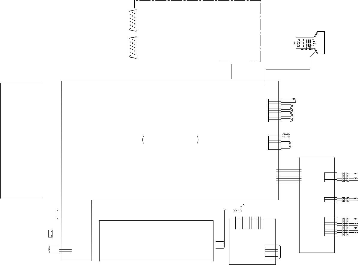
4-2. FRAME SCHEMATIC DIAGRAM
|
CN1101 |
|
|
|
CN502 |
|
|
40P |
|
|
|
40P |
|
|
|
|
|
|
|
|
|
|
40 |
XSC |
XSC |
40 |
|
|
|
39 |
YSC |
YSC |
39 |
|
|
|
38 |
D.TILT |
D.TILT |
38 |
|
|
|
37 |
XDC |
XDC |
37 |
|
|
|
36 |
HFBP |
HFBP |
36 |
|
|
|
35 |
YDC |
YDC |
35 |
|
|
|
34 |
HD OUT |
HD OUT |
34 |
|
|
|
33 |
REFDC |
REFDC |
33 |
|
|
|
32 |
HSHAPE |
HSHAPE |
32 |
|
|
|
31 |
+12V |
+12V |
31 |
|
|
|
30 |
NC |
NC |
30 |
|
|
|
29 |
+12V |
+12V |
29 |
|
|
|
28 |
A.GND |
A.GND |
28 |
|
|
|
27 |
3.3V |
3.3V |
27 |
|
|
|
26 |
D.GND |
D.GND |
26 |
|
|
|
25 |
D.GND |
D.GND |
25 |
|
|
|
24 |
HSAW_SW |
HSAW_SW |
24 |
|
|
|
23 |
GXSC |
GXSC |
23 |
|
|
|
22 |
LCC NS |
LCC NS |
22 |
|
DA (DPU) |
|
21 |
GYSC |
GYSC |
21 |
|
|
20 |
IIC SDA |
IIC SDA |
20 |
|
|
|
18 |
A.GND |
A.GND |
18 |
|
|
|
|
19 |
IIC SCL |
IIC SCL |
19 |
|
|
|
|
|
|
|
|
|
|
17 |
A.GND |
A.GND |
17 |
|
|
|
16 |
H.LINBAL |
H.LINBAL |
16 |
|
|
|
15 |
H BLK |
H BLK |
15 |
|
|
|
14 |
NC |
NC |
14 |
|
|
|
13 |
HS OUT |
HS OUT |
13 |
|
|
|
12 |
DCC2 |
DCC2 |
12 |
|
|
|
11 |
VS OUT |
VS OUT |
11 |
|
|
|
10 |
VSAWN |
VSAWN |
10 |
|
|
|
9 |
NC |
NC |
9 |
|
|
|
8 |
A.GND |
A.GND |
8 |
|
|
|
7 |
PLL LOCK |
PLL LOCK |
7 |
|
|
|
6 |
A.GND |
A.GND |
6 |
|
|
|
5 |
POC |
POC |
5 |
|
|
|
4 |
A.GND |
A.GND |
4 |
|
|
|
3 |
A.GND |
A.GND |
3 |
|
|
|
|
|
|
|
|
|
|
2 |
V.DF |
V.DF |
2 |
|
|
|
1 |
H.DF |
H.DF |
1 |
|
|
|
|
|
|
|
CN1101 |
|
|
|
|
|
|
4P |
|
|
|
|
|
|
WHT |
|
|
|
|
|
1 |
D GND |
|
|
TO ECS |
2 |
+5V |
||
|
|
3 |
RXD |
|||
|
|
|
|
|
4 |
TXD |
|
|
|
|
|
|
CN602 |
|
|
|
|
|
|
3P |
|
|
|
|
|
|
WHT |
|
AC IN |
:VH |
||||
|
|
|
|
|
|
|
|
|
|
|
|
1 |
AC L |
|
|
|
|
|
||
|
|
|
|
|
2 |
NC |
|
|
|
|
|
3 |
AC N |
|
|
|
|
|
||
|
|
|
||||
|
|
|
|
|
||
|
|
|
|
|
|
CN601 |
|
|
|
|
|
|
4P |
|
|
|
|
|
|
WHT |
|
|
|
|
|
|
:VH |
|
|
|
|
|||
|
|
|
|
|
1 |
DGC |
DGC |
|
|
|
|
2 |
NC |
|
|
|
|
3 |
NC |
|
|
|
|||||
|
|
4 |
DGC |
|||
|
||||||
|
|
|
|
10 |
|
|
|
|
|
|
|
|
|
|
|
|
|
|
|
|
|
|
|
|
|
|
|
|
|
|
|
|
|
|
|
|
|
|
|
|
|
|
|
|
|
|
|
|
|
|
15 |
5 |
|
|
|
|
|
|
|
|
|
|
|
|
|
|
|
|
|
|
|
|
|
|
|
|
|
|
|
|
|
|
|
|
|
|
|
|
|
|
|
|
|
|
|
|
|
|
14 9 4 |
|
|
|
|
|
|
|
|
|
|
|
|
|
|
|
|
|
|
|
|
|
|
|
|
|
|
|
|
|
|
|
|
|
|
|
|
|
|
|
|
|
|
|
|
|
CN309 |
13 8 3 |
|
|
|
|
|
|
|
|
|
|
|
|
|
|
|
A1 (VIDEO AMP, RGB OUT ) |
|||||||||||||||||||||||||||||
HD15D-SUB |
|
|
|
|
|
|
|
|
|
|
|
|
|
|
|
||||||||||||||||||||||||||||||||
|
|
|
|
|
|
|
|
|
|
|
|
|
|
|
|
|
|
|
|
||||||||||||||||||||||||||||
|
INPUT2 |
|
12 7 2 |
|
|
|
|
|
|
|
|
|
|
|
|
|
|
|
|||||||||||||||||||||||||||||
|
(HD15) |
|
|
|
|
|
|
|
|
|
|
|
|
|
|
|
|
||||||||||||||||||||||||||||||
|
|
|
11 6 1 |
|
|
|
|
|
|
|
|
|
|
|
|
|
|
|
|||||||||||||||||||||||||||||
|
|
|
|
|
|
|
|
|
|
|
|
|
|
|
|
|
|
|
|
|
|
|
|
|
|
|
|
|
|
|
|
|
|
|
|
|
|
|
|
|
|
|
|
|
|
||
|
|
|
|
10 |
|
|
|
|
|
|
|
|
|
|
|
|
|
|
|
|
|
|
|
|
|
|
|
|
|
|
|
|
|
|
|
|
|
|
|
|
|
|
|
|
|
|
|
|
|
|
|
|
|
|
|
|
|
|
|
|
|
|
|
|
|
|
|
|
|
|
|
|
|
|
|
|
|
|
|
|
|
|
|
|
|
|
|
|
|
|
|
|
|
|
|
|
|
|
|
|
|
|
|
|
|
|
|
|
|
|
|
|
|
|
|
|
|
|
|
|
|
|
|
|
|
|
|
|
|
|
|
|
|
|
|
|
|
|
|
|
|
|
|
|
|
|
15 |
5 |
|
|
|
|
|
|
|
|
|
|
|
|
|
|
|
|
|
|
|
|
|
|
|
|
|
|
|
|
|
|
|
|
|
|
|
|
|
|
|
|
|
|
|
|
|
|
14 9 4 |
|
|
|
|
|
|
|
|
|
|
|
|
|
|
|
|
|
|
|
|
|
|
|
|
|
|
|
|
|
|
|
|
|
|
|
|
|
|
|
|
|
|
|
|
|
CN307 |
13 8 3 |
|
|
|
|
|
|
|
|
|
|
|
|
|
|
|
|
|
|
|
|
|
|
|
|
|
|
|
|
|
|
|
|
|
|
|
|
|
|
|
|
|
|
|
||
HD15D-SUB |
|
|
|
|
|
|
|
|
|
|
|
|
|
|
|
|
|
|
|
|
|
|
|
|
|
|
|
|
|
|
|
|
|
|
|
|
|
|
|
|
|
|
|
||||
|
INPUT1 |
|
12 7 2 |
|
|
|
|
|
|
|
|
|
|
|
|
|
|
|
|
|
|
|
|
|
|
|
|
|
|
|
|
|
|
|
|
|
|
|
|
|
|
|
|
|
|
|
|
|
(HD15) |
|
|
|
|
CN312 |
|
|
|
|
|
|
|
|
|
|
|
CN311 |
|
|
|
|
|
|
|
|
|
|
|
|
|
|
|
|
|
|
|
|
|
|
|
|
|
|
|
||
|
|
|
11 6 1 |
|
|
|
5V |
3.3V |
7V |
+12V |
GND |
+80V |
NC |
+B |
+B |
GND |
SDAIIC |
SCAIIC |
GND |
SWECO |
GND |
SDA1DDC |
SCL1DDC |
GND1DDC |
SDA2DDC |
SCL2DDC |
GND2DDC |
GND |
SWINPUT |
OUTVS |
OUTHS |
BLKH |
|||||||||||||||
|
|
|
|
|
|
|
|
9P |
17P |
||||||||||||||||||||||||||||||||||||||
|
|
|
|
|
|
|
|
WHT |
|
|
|
|
|
|
|
|
|
|
|
WHT |
|
|
|
|
|
|
|
|
|
|
|
|
|
|
|
|
|
|
|
|
|
|
|
|
|
|
|
|
|
|
|
|
|
|
|
|
|
|
|
|
|
|
|
|
|
|
|
|
|
|
|
|
|
|
|
|
|
|
|
|
|
|
|
|
|
|
|
|
|
|
|
|
|
|
|
|
|
|
|
|
|
|
|
|
|
|
|
|
|
|
|
|
|
|
|
|
|
|
|
|
|
|
|
|
|
|
|
|
|
|
|
|
|
|
|
|
|
|
|
|
|
|
|
|
|
|
|
|
|
|
|
|
9 |
8 |
7 |
6 |
5 |
4 |
3 |
2 |
1 |
|
17 |
16 |
15 |
14 |
13 |
12 |
11 |
10 |
9 |
8 |
7 |
6 |
5 |
4 |
3 |
2 |
1 |
||||||||||||
|
|
|
|
|
|
|
|
|
|
|
|
|
|
|
|
|
|
|
|
|
|
|
|
|
|
|
|
|
|
|
|
|
|
|
|
|
|
|
|
|
|
|
|
|
|
|
|
|
|
|
|
|
|
|
|
|
9 |
8 |
7 |
6 |
5 |
4 |
3 |
2 |
1 |
|
17 |
16 |
15 |
14 |
13 |
12 |
11 |
10 |
9 |
8 |
7 |
6 |
5 |
4 |
3 |
2 |
1 |
||||||||||||
|
|
|
|
|
|
|
|
CN604 |
5V |
3.3V |
7V |
+12V |
GND |
+80V |
NC |
+B |
+B |
CN1102 |
GND |
IIC SDA |
IIC SCA |
GND |
ECO SW |
GND |
DDC SDA1 |
DDC SCL1 |
DDC GND1 |
DDC SDA2 |
DDC SCL2 |
DDC GND2 |
GND |
INPUT SW |
VS OUT |
HS OUT |
H BLK |
||||||||||||
|
|
|
|
|
|
|
|
9P |
|
|
|
|
|
|
|
|
|
|
|
17P |
|
|
|
|
|
|
|
|
|
|
|
|
|
|
|
|
|
|
|
|
|
|
|
|
|
|
|
|
|
|
|
|
|
|
|
BLK |
|
|
|
|
|
|
|
|
|
|
|
BLK |
|
|
|
|
|
|
|
|
|
|
|
|
|
|
|
|
|
|
|
|
|
|
|
|
|
|
|
|
|
|
|
|
|
|
|
|
|
|
|
|
|
|
|
|
|
|
|
|
|
|
|
|
|
|
|
|
|
|
|
|
|
|
|
|
|
|
|
|
|
|
|
|
|
|
|
D
DEFLECTION,HDF,VDF,
HV, POWER SUPPLY
CN1104
44P
|
44 |
43 |
42 |
41 |
40 |
39 |
38 |
37 |
36 |
35 |
34 |
33 |
32 |
31 |
30 |
29 |
28 |
27 |
26 |
25 |
24 |
23 |
22 |
21 |
20 |
19 |
18 |
17 |
16 |
15 |
14 |
13 |
12 |
11 |
10 |
9 |
8 |
7 |
6 |
5 |
4 |
3 |
2 |
1 |
|
|
|
NC |
GND |
NC |
NC |
POC |
PLL LOCK |
GND |
S7 |
WAKE UP |
KEY SCAN |
IK SIGMA |
LED1 |
LB DET |
LED2 |
V.FBP |
INPUT SW |
S0 |
+5V |
S1 |
DGC SW |
S2 |
PWR SW |
GND |
HTR SW |
GND |
GND |
S3 |
DDC GND2 |
S4 |
DDC SCL2 |
S5 |
DDC SDA2 |
S6 |
DDC GND1 |
G2 |
DDC SCL1 |
ABL DET |
DDC SDA1 |
HV DET |
ECO SW |
RXD |
IIC SCL |
TXD |
IIC SDA |
|
|
|
|
|
|
|
|
|
|
|
|
|
|
|
|
|
|
|
|
|
|
|
|
|
|
|
|
|
|
|
|
|
|
|
|
|
|
|
|
|
|
|
|
|
|
|
|
|
|
NC |
GND |
NC |
NC |
POC |
PLL LOCK |
GND |
S7 |
WAKE UP |
KEY SCAN |
IK SIGMA |
LED1 |
LB DET |
LED2 |
V.FBP |
INPUT SW |
S0 |
+5V |
S1 |
DGC SW |
S2 |
PWR SW |
GND |
HTR SW |
GND |
GND |
S3 |
DDC GND2 |
S4 |
DDC SCL2 |
S5 |
DDC SDA2 |
S6 |
DDC GND1 |
G2 |
DDC SCL1 |
ABL DET |
DDC SDA1 |
HV DET |
ECO SW |
RXD |
IIC SCL |
TXD |
IIC SDA |
|
|
|
|
|
|
|
|
|
|
|
|
|
|
|
|
|
|
|
|
|
|
|
|
|
|
|
|
|
|
|
|
|
|
|
|
|
|
|
|
|
|
|
|
|
|
|
|
|
|
44 |
43 |
42 |
41 |
40 |
39 |
38 |
37 |
36 |
35 |
34 |
33 |
32 |
31 |
30 |
29 |
28 |
27 |
26 |
25 |
24 |
23 |
22 |
21 |
20 |
19 |
18 |
17 |
16 |
15 |
14 |
13 |
12 |
11 |
10 |
9 |
8 |
7 |
6 |
5 |
4 |
3 |
2 |
1 |
|
|
CN1001 |
|
|
|
|
|
|
|
|
|
|
|
|
|
|
|
|
|
|
|
|
|
|
|
|
|
|
|
|
|
|
|
|
|
|
|
|
|
|
|
|
|
|
|
|
|
|
44P |
|
|
|
|
|
|
|
|
|
|
|
|
|
|
|
|
|
|
|
|
|
|
|
|
|
|
|
|
|
|
|
|
|
|
|
|
|
|
|
|
|
|
|
|
|
|
|
|
|
|
|
|
|
|
|
|
|
|
|
|
|
|
|
|
|
|
|
|
|
|
|
|
|
|
|
|
|
|
|
|
|
|
|
|
|
|
|
|
|
|
CN1003 |
|
|
|
|
|
|
|
|
|
|
|
|
|
|
|
|
|
|
|
|
|
|
|
|
|
|
|
|
|
|
|
|
|
|
|
|
|
|
|
|
|
|
|
|
|
|
6P |
|
|
|
|
|
|
|
|
|
|
|
|
|
|
|
|
|
|
|
|
|
|
|
|
|
|
|
|
|
|
|
|
|
|
|
|
|
|
|
|
|
|
|
|
|
:S-MICRO (L) |
|
||
|
|
|
|
|
|
|
|
|
|
|
|
|
|
|
|
|
|
|
N ( |
|
|
|
|
|
|
|
|
|
|
|
|
|
|
|
|
|
|
|
|
|
|
|
|
|||
|
|
|
|
|
|
|
|
|
|
|
|
|
|
|
|
|
|
|
-COM) |
|
|
|
|
|
|
|
|
|
|
|
|
|
|
|
|
|
GND |
1 |
||||||||
|
|
|
|
|
|
|
|
|
|
|
|
|
|
|
|
|
|
|
|
|
|
|
|
|
|
|
|
|
|
|
|
|
|
|
|
VY |
3 |
|||||||||
|
|
|
|
|
|
|
|
|
|
|
|
|
|
|
|
|
|
|
|
|
|
|
|
|
|
|
|
|
|
|
|
|
|
|
|
|
|
|
|
|
|
|
|
|
VX |
2 |
|
|
|
|
|
|
|
|
|
|
|
|
|
|
|
|
|
|
|
|
|
|
|
|
|
|
|
|
|
|
|
|
|
|
|
|
|
|
|
|
|
|
|
|
|
|
|
|
|
|
|
|
|
|
|
|
|
|
|
|
|
|
|
|
|
|
|
|
|
|
|
|
|
|
|
|
|
|
|
|
|
|
|
|
|
|
|
|
|
|
|
|
T_AMB |
4 |
|
|
|
|
|
|
|
|
|
|
|
|
|
|
|
|
|
|
|
|
|
|
|
|
|
|
|
|
|
|
|
|
|
|
|
|
|
|
|
|
|
|
|
|
LUMI (NC) |
5 |
|
|
|
|
|
|
|
|
|
|
|
|
|
|
|
|
|
|
|
|
|
|
|
|
|
|
|
|
|
|
|
|
|
|
|
|
|
|
|
|
|
|
|
|
|
|
5V (NC) |
6 |
CN318 |
2P |
G2 |
G2(NC) |
|
|
|
|
|
|
|
|
1 |
2 |
|
|
|
|
|
|
|
|
HV |
|
|
|
|
1 |
|
|
|
|
CN504 1P |
1.2kV |
|
|
|
|
|
|
|
|
||
|
|
|
|
|
|
|
|
|
|
|
|
|
|
CN1103 |
SWINPUT |
+5V |
GND |
2LED |
1LED |
SCANKEY |
UPWAKE |
+12V |
||||||||||||
|
|
|
|
|
|
|
|
|
8P |
|
|
|||||||||||||||||
|
|
|
|
|
|
|
|
|
WHT |
|
|
|
|
|
|
|
|
|
|
|
|
|
|
|
|
|
|
|
|
|
|
|
|
|
|
|
|
|
|
|
|
|
|
|
|
|
|
|
|
||||||||
|
|
|
|
|
|
|
|
|
|
|
|
|
8 |
7 |
6 |
5 |
4 |
3 |
2 |
1 |
||||||||
|
|
|
|
|
|
|
|
|
|
|
|
|
|
|
|
|
|
|
|
|
|
|
|
|
|
|
|
|
|
|
|
|
|
|
|
|
|
|
|
|
|
|
|
|
|
|
|
|
|
|
|
|
|
|
|
|
|
|
|
|
|
|
|
|
|
|
|
|
|
|
|
|
|
|
|
|
|
|
|
|
|
|
|
|
|
|
|
|
|
|
|
|
|
|
|
|
|
|
|
|
|
|
|
|
|
|
|
|
|
|
|
|
|
|
|
|
|
|
|
|
|
|
|
|
|
|
|
|
|
|
|
|
|
|
|
|
|
|
|
|
|
|
|
|
|
14 |
13 |
12 |
11 |
10 |
9 |
8 |
7 |
6 |
5 |
4 |
3 |
2 |
1 |
||||||||||||||
|
VX |
VY |
T AMB |
GND |
GND |
GND |
INPUT SW |
+5V |
GND |
LED 2 |
LED 1 |
KEY SCAN |
WAKE UP |
+12V |
||||||||||||||
|
|
|
|
|
|
|
|
|
|
|
|
|
|
|
|
|
|
|
|
|
|
|
|
|
|
|
|
|
H3
(USER CONTROL)
HG |
PICTURE |
H |
|
|
TUBE |
RGB |
G1 G2 |
CN701 |
|
|
|
10P |
|
|
|
WHT |
|
|
|
:S-MICRO |
|
ROTATION |
|
|
|
||
ROTATION+ |
10 |
|
|
ROTATION– |
9 |
|
|
XSC– |
8 |
|
|
XSC+ |
7 |
|
|
YSC– |
6 |
|
|
YSC+ |
5 |
|
|
XDC– |
4 |
|
|
XDC+ |
3 |
|
|
YDC– |
2 |
|
|
YDC+ |
1 |
|
|
CN501 |
|
|
|
6P |
|
|
|
WHT |
|
|
|
:VH |
|
|
|
V+ |
1 |
V DY |
|
V– |
2 |
|
|
NC |
3 |
|
|
H– |
4 |
H DY |
|
NC |
5 |
||
|
|||
H+ |
6 |
|
CN1603
CN1101
40P
1 |
-15V |
-15V |
1 |
2 |
+15V |
+15V |
2 |
3 |
GND |
GND |
3 |
4 |
GXSC |
GXSC |
4 |
5 |
GYSC |
GYSC |
5 |
6 |
LCC_NS |
LCC_NS |
6 |
7 |
IIC SDA |
IIC SDA |
7 |
8 |
IIC SCL |
IIC SCL |
8 |
CN1400
14P
CN1401
5P
GND |
1 |
|
|
VX |
2 |
|
|
VY |
3 |
TO |
|
MAGNETIC |
|||
T_AMB |
4 |
||
SENSOR |
|||
|
|
||
LUMI (NC) |
5 |
|
|
5V (NC) |
6 |
|
8P |
|
|
WHT |
CN1601 |
|
|
|
|
|
4P |
|
|
WHT |
|
|
:S-MICRO |
|
|
CY4+ |
3 |
|
CY4– |
4 |
|
CY3+ |
1 |
|
CY3– |
2 |
|
CN1600 |
|
|
2P |
|
|
WHT |
|
|
:S-MICRO |
|
|
LCC-NS (+) |
1 |
|
LCC-NS (–) |
LCC-NS |
|
2 |
|
|
CN1602 |
|
|
LCC-LT (+) |
1 |
|
LCC-LT (–) |
LCC-LT |
|
2 |
|
|
LCC-LB (+) |
3 |
|
LCC-LB (–) |
LCC-LB |
|
4 |
|
|
LCC-RT (+) |
5 |
|
LCC-RT (–) |
LCC-RT |
|
6 |
|
|
LCC-RB (+) |
7 |
|
LCC-RB (–) |
LCC-RB |
|
8 |
L2 (CY, LCC)
B-SS9342<AEP>-KESSENZU-EPS05
21T3 (E) 4-4
Loading...