


 Loading...
Fiber Optic “Light to Logic” Receiver with Clock Recovery
Preliminary Technical Data
Features
•Light to Logic 20-Pin DIP Receiver Offers ECL Compatibility
•Sensitivity:
–31 dBm
•Phase-Locked Loop (PLL) Timing Recovery Circuit
•Meets All SONET Jitter Requirements
(CCITT G.958)
•Single +5 V Supply, Typically <1.00 W
•SONET/SDH Compliant
Applications
•Telecommunication Networks
•SONET OC12 and SDH STM4 Compatible
•Local and Metropolitan Area Networks
•ATM Single Mode Public Network
•Military Communications and Control Systems
•Digital Cable TV Networks
RGR2622
Description
The RGR2622 receiver provides optical signal conversion and processing. It converts 1200 nm to 1600 nm wavelength lightwave information into an electrical signal at data rates of 622 Mb/s.
Each receiver contains an InGaAs PIN photodiode, a high sensitivity, wide dynamic range transimpedance amplifier, capacitively coupled to a PLL based clock recovery circuit. The clock and data outputs are retimed complementary PECL.
A complementary CMOS compatible low light alarm is also provided.
Preliminary Product Disclaimer
This preliminary data sheet is provided to assist you in the evaluation of engineering samples of the product which is under development. Until Hewlett-Packard releases this product for general sales, HP reserves the right to alter prices, specifications, features, capabilities, function, manufacturing release dates, and even general availability of the product at any time.
406 |
(5/97) |
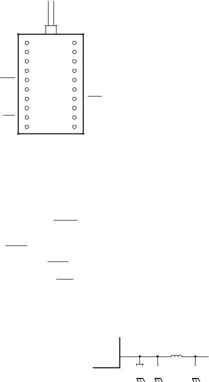
Connection Diagram
Top View
|
|
FIBER PIGTAIL |
|
GND |
1 |
20 |
NC |
GND |
2 |
19 |
NC |
GND |
3 |
18 |
NC |
CLOCK |
4 |
17 |
NC |
CLOCK |
5 |
16 |
GND |
GND |
6 |
15 |
GND |
DATA |
7 |
14 |
ALARM |
GND |
8 |
13 |
GND |
DATA |
9 |
12 |
ALARM |
PD BIAS |
10 |
11 |
+5 V |
Pin Descriptions
Pins 1, 2, 3, 6, 8, 13, 15, 16,
GND:
These pins should be connected to the circuit ground.
Pins 4, 5, CLOCK, CLOCK:
These pins provide complementary PECL CLOCK
and CLOCK outputs.
Pins 7, 9, DATA, DATA:
These pins provide complementary PECL DATA and DATA outputs.
The RGR2622 DATA output is noninverting, an optical pulse causes the DATA output to go to
|
|
|
|
|
|
the PECL logic high state (+4 V |
Pins 12, 14, ALARM, ALARM: |
||||
nominal). |
These pins provide complemen- |
||||
Pin 10, PD Bias: |
tary ALARM and |
ALARM |
outputs. |
||
|
|
|
|
|
|
This pin must be connected to any voltage from 0 V (GND) to –5 V. This provides the photodiode bias. The current drawn is directly proportional to the average received photocurrent.
I = Responsivity x Mean Power.
The Responsivity will be between 0.8 A/W and 1.0 A/W.
Pin 11, +5 V:
This pin should be connected to +5 V supply. The network shown below should be placed as close as possible to pin 11.
This is the low light alarm. ALARM goes to a logic low (CMOS compatible) state when the optical power drops below the threshold level (insufficient optical power).
The optical power must increase to a higher level than the level where the alarm went low before ALARM will return to a logic high. This difference is the alarm hysteresis.
Pins 17, 18, 19, 20 NC:
These pins are not connected.
1 µH
 +5 V
+5 V
PIN 11
10 µF |
|
|
|
|
|
100 nF |
|
|
100 nF |
|
|
|
|
|
|
|
|
|
|
407
Loading...