


TF219..B
TF219..B
Fast Switching Thyristor
Replaces March 1998 version, DS4271-2.3 |
DS4271-3.0 January 2000 |
APPLICATIONS
■High Power Inverters And Choppers
■UPS
■Railway Traction
■Induction Heating
■AC Motor Drives
■Cycloconverters
FEATURES
■Double Side Cooling
■High Surge Capability
■High Voltage
VOLTAGE RATINGS
Type Number |
Repetitive |
Conditions |
|
Peak |
|
|
Voltages |
|
|
VDRM VRRM |
|
TF219 20B |
2000 |
VRSM = VRRM + 100V |
TF219 18B |
1800 |
|
TF219 16B |
1600 |
IDRM = IRRM = 15mA |
TF219 14B |
1400 |
|
|
|
at VRRM or VDRM & Tvj |
|
|
|
Lower voltage grades available. |
|
|
KEY PARAMETERS
|
|
|
|
|
|
|
|
|
|
VDRM |
2000V |
|||
|
|
|
|
|
|
|
|
|
|
IT(RMS) |
190A |
|||
|
|
|
|
|
|
|
|
|
|
ITSM |
1200A |
|||
|
|
|
|
|
|
|
|
|
|
dV/dt |
200V/μs |
|||
|
|
|
|
|
|
|
|
|
|
dI/dt |
500A/μs |
|||
|
|
|
|
|
|
|
|
|
|
tq |
40μs |
|||
|
|
|
|
|
|
|
|
|
|
|
|
|
|
|
|
|
|
|
|
|
|
|
|
|
|
|
|
|
|
|
|
|
|
|
|
|
|
|
|
|
|
|
|
|
|
|
|
|
|
|
|
|
|
|
|
|
|
|
|
|
|
|
|
|
|
|
|
|
|
|
|
|
|
|
|
|
|
|
|
|
|
|
|
|
|
|
|
|
|
|
|
|
|
|
|
|
|
|
|
|
|
|
|
|
|
|
|
|
|
|
|
|
|
|
|
|
|
|
|
|
|
|
|
|
|
|
|
|
|
|
|
|
|
|
|
|
|
|
|
|
|
|
|
|
|
|
|
|
|
|
|
|
|
|
|
|
|
|
|
|
|
|
|
|
|
|
|
|
|
|
|
|
|
|
|
|
|
|
|
|
|
|
|
|
|
|
|
|
|
|
|
|
|
|
Outline type code: MU86.
See Package Details for further information.
CURRENT RATINGS
Symbol |
Parameter |
Conditions |
Max. |
Units |
||
|
|
|
|
|
||
IT(AV) |
Mean on-state current |
Half sinewave, 50Hz, Tcase = 80oC |
120 |
A |
||
I |
RMS value |
Half sinewave, 50Hz, T |
case |
= 80oC |
190 |
A |
T(RMS) |
|
|
|
|
|
|
1/13
TF219..B
SURGE RATINGS
Symbol |
Parameter |
|
Conditions |
|
|
Max. |
Units |
|
|
|
|
|
|
|
|
||
ITSM |
Surge (non-repetitive) on-state current |
10ms half sine; VR |
= 0% |
VRRM, Tj = 125˚C |
1.2 |
kA |
||
I2t |
I2t for fusing |
10ms half sine; V |
= 0% |
V , T |
j |
= 125˚C |
7.2 |
A2s |
|
|
R |
|
RRM |
|
|
|
|
THERMAL AND MECHANICAL DATA
Symbol |
Parameter |
Conditions |
|
Min. |
Max. |
Units |
|
|
|
|
|
|
|
|
|
|
|
Double side cooled |
dc |
- |
0.1 |
oC/W |
|
|
|
|
|
|
|
|
|
R |
Thermal resistance - junction to case |
|
Anode dc |
- |
0.19 |
oC/W |
|
th(j-c) |
|
Single side cooled |
|
|
|
|
|
|
|
|
|
|
|
||
|
|
Cathode dc |
- |
0.24 |
oC/W |
||
|
|
|
|||||
|
|
|
|
|
|
|
|
|
|
Clamping force 3.5kN |
Double side |
- |
0.02 |
oC/W |
|
Rth(c-h) |
Thermal resistance - case to heatsink |
|
|
|
|
||
with mounting compound |
Single side |
- |
0.04 |
oC/W |
|||
|
|
||||||
|
|
|
|||||
|
|
|
|
|
|
|
|
|
|
On-state (conducting) |
|
- |
125 |
oC |
|
Tvj |
Virtual junction temperature |
|
|
|
|
|
|
Reverse (blocking) |
|
- |
125 |
oC |
|||
|
|
|
|||||
|
|
|
|
|
|
|
|
Tstg |
Storage temperature range |
|
|
-40 |
150 |
oC |
|
- |
Clamping force |
|
|
3.3 |
3.6 |
kN |
|
|
|
|
|
|
|
|
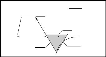
MEASUREMENT OF RECOVERED CHARGE - QRA1
Measurement of QRA1 : QRA1 = IRR x tRR
2
ITM
|
|
|
|
QRA1 |
|
|
|
|
|
|
|
|
|
|
|
|
|
|
tp |
= 1ms |
|
|
0.5x IRR |
|
|
dIR/dt |
|
||
|
|
IRR |
|
||
|
|
|
|
||
2/13
TF219..B
DYNAMIC CHARACTERISTICS
Symbol |
Parameter |
|
|
|
|
|
|
Conditions |
|
|
|
Min. |
Max. |
Units |
|||||
|
|
|
|
|
|
|
|
|
|
||||||||||
VTM |
Maximum on-state voltage |
At 150A peak, Tcase = 25oC |
|
|
|
- |
2.75 |
V |
|||||||||||
I |
/I |
Peak reverse and off-state current |
At V |
|
/V |
, T |
case |
= 125oC |
|
|
|
- |
15 |
mA |
|||||
RRM |
DRM |
|
|
|
RRM DRM |
|
|
|
|
|
|
|
|
|
|
|
|||
|
|
|
|
|
|
|
|
|
|
||||||||||
dV/dt |
Maximum linear rate of rise of off-state voltage |
Linear to 60% V |
|
T = 125oC, Gate open circuit |
- |
200 |
V/μs |
||||||||||||
|
|
|
|
|
|
|
|
DRM |
j |
|
|
|
|
|
|
|
|
|
|
|
|
|
|
|
|
|
|
|
|
||||||||||
dI/dt |
|
Gate source 20V, 20Ω |
|
Repetitive 50Hz |
- |
500 |
A/μs |
||||||||||||
Rate of rise of on-state current |
|
|
|
|
|
|
|
|
|
|
|
|
|
|
|
|
|
||
tr ≤ 0.5μs, Tj = 125˚C |
|
|
|
Non-repetitive |
- |
800 |
A/μs |
||||||||||||
|
|
|
|
|
|
||||||||||||||
|
|
|
|
|
|
|
|
|
|
|
|
|
|
|
|
|
|||
V |
|
Threshold voltage |
At T |
vj |
= 125oC |
|
|
|
|
|
|
|
|
- |
2.0 |
V |
|||
T(TO) |
|
|
|
|
|
|
|
|
|
|
|
|
|
|
|
|
|
||
|
|
|
|
|
|
|
|
|
|
|
|
|
|
||||||
rT |
On-state slope resistance |
At Tvj = 125oC |
|
|
|
|
|
|
|
|
- |
5.0 |
mΩ |
||||||
|
|
|
|
|
|
|
|
|
|
|
|
||||||||
tgd |
Delay time |
Tj = 25˚C, IT = 100A, |
|
|
|
|
|
|
- |
3* |
μs |
||||||||
|
|
|
VD = 50V, IG = 1A, |
|
|
|
|
|
|
|
|
|
|
||||||
|
|
|
|
|
|
|
|
|
|
|
|
|
|||||||
t(ON)TOT |
Total turn-on time |
dI/dt = 50A/μs, dIG/dt = 1A/μs |
|
|
|
- |
1.5* |
μs |
|||||||||||
I |
H |
Holding current |
T |
= 25oC, I |
TM |
= 1A, V |
D |
= 12V |
|
|
|
- |
60 |
mA |
|||||
|
|
j |
|
|
|
|
|
|
|
|
|
|
|
|
|
|
|||
|
|
|
|
|
|
|
|
|
|
||||||||||
|
|
|
Tj = 125˚C, IT = 100A, VR = 50V, |
|
t |
code: B |
- |
40 |
μs |
||||||||||
t |
q |
Turn-off time |
dV/dt = 200V/μs (Linear to 60% VDRM), |
q |
|
|
|
|
|||||||||||
|
|
dIR/dt = 30A/μs, Gate open circuit |
|
|
|
|
|
||||||||||||
|
|
|
|
|
|
|
|
||||||||||||
|
|
|
|
|
|
|
|
|
|
|
|
|
|
|
|
|
|
|
|
*Typical value. |
|
|
|
|
|
|
|
|
|
|
|
|
|
|
|
|
|
||
GATE TRIGGER CHARACTERISTICS AND RATINGS |
|
|
|
|
|
|
|
|
|
|
|
|
|
||||||
Symbol |
Parameter |
|
|
|
|
Conditions |
Typ. |
Max. |
Units |
||||||||
|
|
|
|
|
|
|
|
|
|
|
|
|
|
||||
V |
GT |
Gate trigger voltage |
V |
DRM |
= 12V, T |
= 25oC, R |
L |
= 6Ω |
- |
3.0 |
V |
||||||
|
|
|
|
|
case |
|
|
|
|
|
|
|
|||||
|
|
|
|
|
|
|
|
|
|
|
|
|
|
||||
I |
GT |
Gate trigger current |
V |
DRM |
= 12V, T |
= 25oC, R |
L |
= 6Ω |
- |
200 |
mA |
||||||
|
|
|
|
case |
|
|
|
|
|
|
|
|
|||||
|
|
|
|
|
|
|
|
|
|
|
|
||||||
V |
GD |
Gate non-trigger voltage |
At V |
|
T |
= 125oC, R |
L |
= 1kΩ |
- |
0.2 |
V |
||||||
|
|
|
|
|
DRM |
case |
|
|
|
|
|
|
|
|
|||
|
|
|
|
|
|
|
|
|
|
|
|
|
|
|
|
||
VRGM |
Peak reverse gate voltage |
|
|
|
|
|
|
|
|
|
|
|
- |
5.0 |
V |
||
IFGM |
Peak forward gate current |
Anode positive with respect to cathode |
- |
4 |
A |
||||||||||||
PGM |
Peak gate power |
|
|
|
|
|
|
|
|
|
|
|
- |
16 |
W |
||
PG(AV) |
Mean gate power |
|
|
|
|
|
|
|
|
|
|
|
- |
3 |
W |
||
3/13

TF219..B
CURVES
4/13
 Loading...