


P4TSV
FCC Information and Copyright
This equipment has been tested and found to c omply with the limits of a Class B digital device, pursuant to Part 15 of the FCC Rules . T hese limits
are designed to provide reasonable protection agains t harmful
interference in a residential installation. This equipment generates , uses and can radiate radio frequency energy and, if not ins talled and used in
accordance with the instructions, may c ause harmful interference to radio
communications .There is no guarantee that interference will not occur in a partic ular installation.
The vendor makes no representations or warranties with respec t to the contents here of and specially disclaims any implied warranties of merchantability or fitness for any purpose. Further the vendor reserves
the right to revise this publication and to make changes to the c ontents
here of without obligation to notify any party beforehand.
Duplication of this publication, in part or in whole, is not allowed without firs t obtaining the vendor’s approval in writing.
The c ontent of this user’s manual is subject to be changed without notice and we will not be responsible for any mistakes found in this us er’s
manual. All the brand and product names are trademarks of their respective c ompanies .
i

Content |
|
LAYOUT OF P4TSV................................................................................. |
1 |
COMPONENT INDEX............................................................................. |
2 |
ENGLISH................................................................................................... |
3 |
P4TSV Features......................................................................................... |
3 |
Package contents....................................................................................... |
5 |
How to set up Jumper................................................................................. |
5 |
CPU Installation......................................................................................... |
5 |
DDR DIMM Modules: DDRA1-2, DDRB1-2 ...................................................... |
6 |
Installing DDR Module................................................................................ |
7 |
Jumpers, Headers, Connectors & Slots......................................................... |
7 |
ESPAÑOL ................................................................................................ |
14 |
Características del P4TSV......................................................................... |
14 |
Contenido del Paquete............................................................................. |
16 |
Cómo instalar un Puente........................................................................... |
16 |
Instalación del CPU.................................................................................. |
16 |
Módulos DDR DIMM: DDRA1-2, DDRB1-2.................................................... |
17 |
Instalación del Módulo DDR ...................................................................... |
18 |
Puentes, Cabezales, Conectores y Ranuras ................................................ |
19 |
DEUTSCH................................................................................................ |
26 |
Spezifikationen von P4TSV........................................................................ |
26 |
Verpackungsinhalt................................................................................... |
28 |
Einstellung der Jumper............................................................................. |
28 |
Installation der CPU.................................................................................. |
28 |
DDR DIMM Modules: DDRA1-2, DDRB1-2 .................................................... |
29 |
Installation von DDR-Modul....................................................................... |
30 |
Jumpers, Headers, Anschlüsse & Slots....................................................... |
30 |
WARPSPEEDER..................................................................................... |
37 |
Introduction............................................................................................. |
37 |
System Requirement................................................................................ |
37 |
Installation .............................................................................................. |
38 |
Usage..................................................................................................... |
39 |
TROUBLE SHOOTING......................................................................... |
47 |
SOLUCIÓN DE PROBLEMAS ............................................................. |
48 |
PROBLEMLÖSUNG.............................................................................. |
49 |
ii
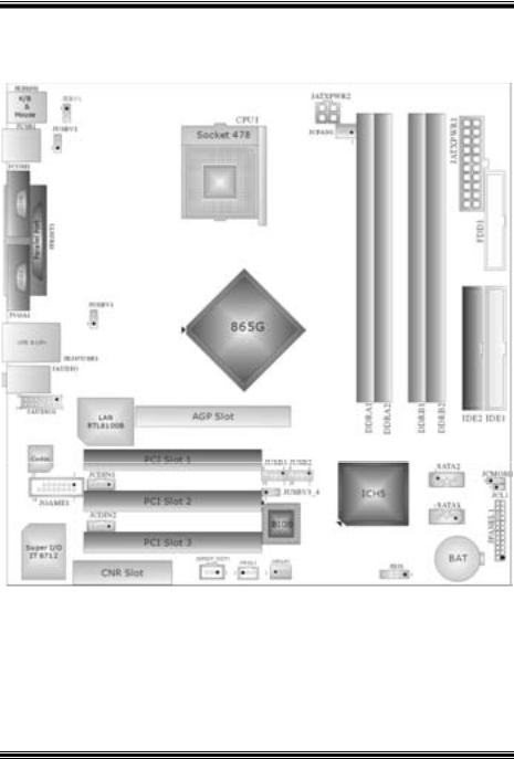
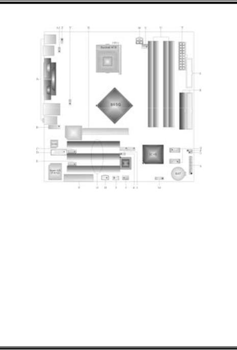
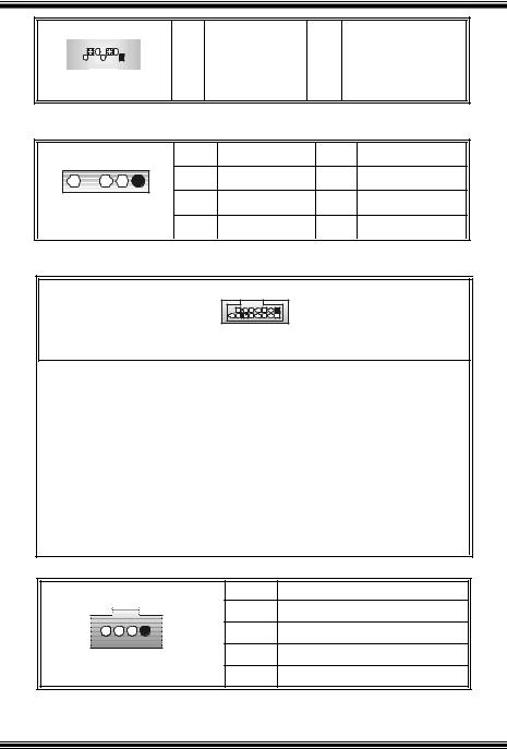
Layout of P4TSV
NOTE: ●represents the f irst pin.
1
Component Index
A. Back Panel Connectors |
O. JCL1: Case Open Connector |
B. JAUDIO1: Front Audio Header |
P. JCMOS:Clear CMOS Jumper |
C. JCDIN1: CD-Rom Audio-In Header |
Q. SATA1-2: Serial ATA Connectors |
D. JGAME1: Game Header |
R. IDE1-2: Hard Disk Connectors |
E. JCDIN2: CD-ROM Audio-In Header |
S. FDD1: Floppy Disk Connector |
F. CNR1: Communication NetworkT. JATXPWR1: ATX Power Connector
Riser Slot
G.PCI1-3: Peripheral ComponentU. DDRA1-2/ DDRB1-2: DDR DIMM
Interconnect Slots |
Modules |
|
|
|
||
H. JSPDIF_OUT1: Digital Audio V. JCFAN: CPU Fan Connector |
|
|||||
Connector |
W. |
JATXPWR2: |
ATX |
Power |
||
I. JWOL1: Wake On LAN Header |
||||||
Connector |
|
|
|
|||
|
|
|
|
|||
J. JSFAN1: System Fan Header |
X. AGP1: Accelerated Graphics Port |
|||||
Slot |
|
|
|
|||
|
|
|
|
|||
K. JUSBV3_4: 5V/5VSB Selection |
for Y. JUSBV2: 5V/5VSB |
Selection |
for |
|||
JUSBV2/3 |
JRJ45USB1 |
|
|
|
||
L. JUSB2/3: Front USB Headers |
Z. |
JKBV1: 5V/5VSB |
Selection |
for |
||
Keyboard |
|
|
|
|||
|
|
|
|
|||
M. JDJ1: Audio DJ Connector |
A1. |
JUSBV1: 5V/5VSB Selection for |
||||
JUSB1 |
|
|
|
|||
|
|
|
|
|||
N. JPANEL1 : Front Panel Connector
2

English
P4TSV Features
A. Hardware
CPU
 Prov ides Socket-478.
 Supports the Intel Pentium 4 processor up to 3.06GHz.
 Front Side Bus at 400/533/800MHz.
 Supports Hy per-Threading.
 Supports Northwood and Prescott CPU. (Willamette not supported)
Chipset
 North Bridge: Intel 865G.
 South Bridge: Intel ICH5.
Main Memory
 Supports one or two 64-bit wide DDR data channels with 1 or 2 DIMMs
per-channel.
 Available bandwidth up to 3.2GB/s(DDR400) f or single-channel mode and 6.4GB/s (DDR 400) in dual channel mode.
 Supports 128-MB, 256-Mb, 512-Mb and 1-GB DDR technologies.
 Supports only x8, x16 DDR dev ices.( Does not support registered DIMMs or double sided X 16 DIMMs)
 Supports four bank devices.
  Maximum memory size is 4GB.
Super I/O
 Chip: ITE IT8712F.
 Low Pin Count Interface.
 Prov ides the most commonly used legacy Super I/O functionality.
  Env ironment Control initiatives,
-H/W Monitor
-Fan Speed Controller
-ITE's "Smart Guardian" f unction
Slots
 Three 32-bit PCI bus master slots.
 One CNR slot.
 One AGP 4X/8X slot.
On Board IDE
 Supports four IDE disk drives.
 Supports PIO Mode 5, Bride Mode and Ultra DMA 33/66/100 Bus Master Mode.
  Supports 2 Serial ATA (SATA) ports.
3

-Compliant with SATA 1.0 specification
-Data transfer rates up to 1.5 GB/s
LAN
 Chip: RTL8100B.
 Supports 10 Mb/s and 100 Mb/s auto-negotiation.
 Half /Full duplex capability.
 Supports ACPI power management.
On Board AC’97 Sound Codec
 Chip: CMI9739A.
 Compliant with AC’97 specification.
 AC97 2.2 interface.
 Supports 6 channels.
On Board Peripherals
a.Rearside
 1 serial port.
 1 parallel port. (SPP/EPP/ECP mode)
 1 VGA port.
 Audio ports in vertical.
 1 RJ-45 LAN jack.
 Supports PS/2 mouse and PS/2 key board.
  4 USB2.0 ports.
b.FrontSide
 1 floppy port supports 2 FDDs with 360K, 720K, 1.2M, 1.44M and 2.88Mbytes.
  4 USB2.0 ports.
Dimensions
 Micro ATX Form Factor: 24.4 X24.4cm (W X L)
B. BIOS & Software
BIOS
 Award legal BIOS.
 Supports APM1.2.
 Supports ACPI.
 Supports USB Function.
Software
 Supports Warpspeeder™, 9th Touch™, FLASHER™, StudioFun! ™ (optional).
 Off ers the highest performance for Windows 98 SE, Windows 2000, Windows Me, Windows XP, SCO UNIX etc.
4

Package contents
 HDD Cable X 2
 FDD Cable X1
 User’s Manual X1
 Fully Setup Driv er CD X1
 StudioFun! Application CD X 1 (optional)
 USB 2.0 Cable X1 (optional)
 S/PDIF Cable X 1 (optional)
 Rear I/O Panel f or Micro ATX Case X1 (optional)
 Serial ATA Cable X1
 Serial ATA Power Switch Cable X1
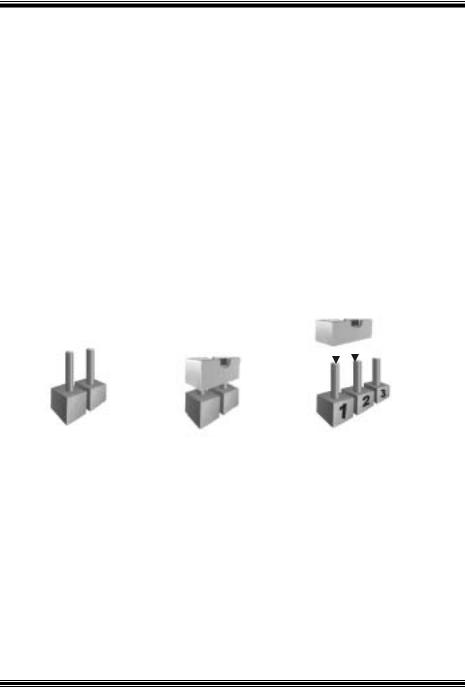
How to set up Jumper
The illustration shows to how set up jumper. When the Jumper cap is placed on pins, the jumper is “close”. IF no jumper cap is placed on the pins, the jumper is ”open”. The
illustration shows a 3-pin jumper whose pin1and 2 are “close” when jumper cap is placed on these 2 pins.
|
|
|
|
|
Jumper open |
Jumper close |
Pin1-2 close |
||
CPU Installation
Step1: Pull the lever sideway s away from the socket and then raise the lev er up to a 90-degree angle.
Step2: Look f or the white dot/cut edge. The white dot/cut edge should point wards the lev er piv ot. The CPU will f it only in the correct orientation.
Step3: Hold the CPU down f irmly, and then close the lever to complete the installation.
Step4: Put the CPU Fan on the CPU and buckle it. Connect the CPU fan power cable to the JCFAN1. This completes the installation.
5
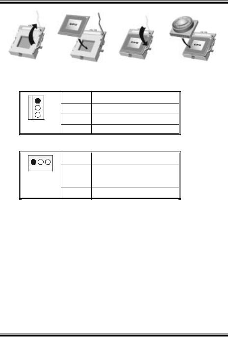
Step1 Step2 Step3 Step4
CPU Fan Headers: JCFAN1
1 |
Pin |
Assignment |
|
|
1 |
Ground |
|
JCFAN1 |
2 |
+12V |
|
3 |
FAN RPM Sense |
||
|
System Fan Headers: JSFAN1
|
Pin |
Assignment |
|
1 |
1 |
Ground |
|
2 |
+12V |
||
JSFAN1 |
|||
|
3 |
FAN RPM Sense |
DDR DIMM Modules: DDRA1-2, DDRB1-2
 Supports up to four DDR DIMMs(two DIMMs per channel), single-sided and/ or double-sides.
 For Dual Channel Operation, DIMMs must be populated in identical pairs. It
has to be the combination of DDRA1+DDRB1 (Blue DIMMs) or DDRA2+DDRB2 (white DIMMs). For more dual channel operation information please log on: www.biostar.com.tw)
DRAM Access Time: 2.5V Unbuffered/ no registered (without ECC) DDR SDRAM PC2100/ PC2700/ PC3200 Ty pe required.
DRAM Ty pe: 128MB/ 256MB/ 512MB/ 1GB DIMM Module (184 pin)
Total Memory Size with Unbuffered/ Registered DIMMs
6

|
|
|
|
|
|
DIMM Socket |
DDR Module |
Total Memory |
|
|
Location |
|
Size (MB) |
|
|
DDRA1 |
64MB/128MB/256MB/512MB/1GB |
|
|
|
|
*1 |
|
|
|
DDRA2 |
64MB/128MB/256MB/512MB/1GB |
|
|
|
|
*1 |
Max is |
|
|
DDRB1 |
64MB/128MB/256MB/512MB/1GB |
4GB |
|
|
|
*1 |
|
|
|
DDRB2 |
64MB/128MB/256MB/512MB/1GB |
|
|
|
|
*1 |
|
|
|
|
|
|
|
|
|
***Only for reference*** |
|
|
Installing DDR Module
1.Unlock a DIMM slot by pressing the retaining clips outward. Align a DIMM on the slot such that the notch on the DIMM matches the break on the slot.
2.Insert the DIMM v ertically and firmly into the slot until the retaining chip snap back in place and the DIMM is properly seated.
Jumpers, Headers, Connectors & Slots
Floppy Disk Connector: FDD1
The motherboard provides a standard f loppy disk connector that supports 360K,
720K, 1.2M, 1.44M and 2.88M floppy disk types. This connector supports the prov ided f loppy drive ribbon cables.
Hard Disk Connectors: IDE1/ IDE2
The motherboard has a 32-bit Enhanced PCI IDE Controller that provides PIO Mode 0~5, Bus Master, and Ultra DMA 33/ 66/ 100 f unctionality. It has two HDD connectors IDE1 (primary) and IDE2 (secondary).
The IDE connectors can connect a master and a slave driv e, so you can connect up to f our hard disk driv es. The f irst hard drive should alway s be connected to
IDE1.
Peripheral Component Interconnect Slots: PCI1-3
This motherboard is equipped with 3 standard PCI slots. PCI stands f or Peripheral Component Interconnect, and it is a bus standard for expansion cards. This PCI slot is designated as 32 bits.
Accelerated Graphics Port Slot: AGP1
Your monitor will attach directly to that v ideo card. This motherboard supports
7

video cards for PCI slots, but it is also equipped with an Accelerated Graphics Port (AGP). An AGP card will take advantage of AGP technology f or improved video
efficiency and performance, especially with 3D graphics.
Communication Network Riser Slot:CNR1
The CNR specification is an open Industry Standard Architecture, and it defines a hardware scalable riser card interf ace, which supports modem only.
Serial ATA Connector: JSATA1/JSATA2
The motherboard has a PCI to SATA Controller with 2 channels SATA interf ace, it satisfies the SATA 1.0 spec and can transf er data with 1.5GHz speed.
Front Panel Connector: JPANEL1
|
|
SLP |
|
PWR_LED ON/OFF |
IR |
|
|
JPANEL1 |
2 |
|
|
|
24 |
|
|
1 |
|
|
|
2 3 |
|
||
|
|
|
|
|
|
||
|
|
SPK |
HLED |
RST |
IR |
|
|
Pin |
Assignment |
Function |
Pin |
Assignment |
Function |
||
1 |
+5V |
|
Speaker |
2 |
Sleep Control |
Sleep |
|
3 |
NA |
|
Connector |
4 |
Ground |
Button |
|
5 |
NA |
|
|
|
6 |
NA |
NA |
7 |
Speaker |
|
|
8 |
Power LED (+) |
POWER |
|
9 |
HDD LED (+) |
Hard Drive |
10 |
Power LED (+) |
LED |
||
11 |
HDD LED (-) |
|
LED |
12 |
Power LED (-) |
|
|
13 |
Ground |
Reset |
14 |
Power Button |
Power-on |
||
15 |
Reset Control |
Button |
16 |
Ground |
Button |
||
17 |
NA |
|
|
|
18 |
KEY |
|
19 |
NA |
|
|
IrDA |
20 |
KEY |
IrDA |
21 |
+5V |
|
Connector |
22 |
Ground |
Connector |
|
23 |
IRTX |
|
|
|
24 |
IRRX |
|
Power Connectors: JATXPWER1/ JATXPWR2
|
|
|
|
|
|
|
|
|
|
|
|
PIN |
Assignment |
PIN |
Assignment |
|
|
|
|
|
1 |
+3.3V |
11 |
+3.3V |
|
|
|
|
|
|
|
|
|
|
|
|
|
|
|
|
|
|
|
|
|
|
|
|
|
|
|
|
|
|
|
|
|
|
|
|
|
|
8
10 |
2 0 |
1 |
11 |
JATXPWR1 |
|
2 |
+3.3V |
12 |
-12V |
3 |
Ground |
13 |
Ground |
4 |
+5V |
14 |
PS_ON |
5 |
Ground |
15 |
Ground |
6 |
+5V |
16 |
Ground |
7 |
Ground |
17 |
Ground |
8 |
PW_OK |
18 |
-5V |
9 |
+5V_SB |
19 |
+5V |
10 |
+12V |
20 |
+5V |
2 |
1 |
PIN |
Assignment |
PIN |
Assignment |
|
3 |
1 |
+12V |
3 |
Ground |
|
|
|
|||
JATXPWR2 |
2 |
+12V |
4 |
Ground |
|
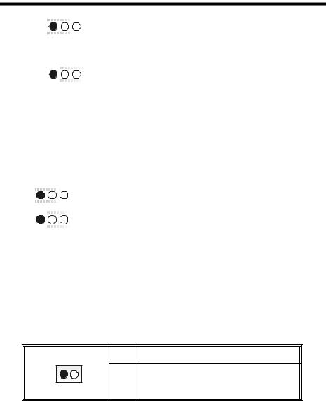
5V / 5VSBSelection for KB: JKBV1
|
|
|
|
|
|
|
|
|
|
JKBV1 |
|
Assignment |
Description |
|
|
|
1 |
|
|
3 |
+5V |
5V for key board and mouse |
|
|
|
|
|
||||
|
|
|
|
|
|
|
|
|
Pin 1-2 close |
|
|
||||
|
|
|
|
||||
|
1 |
|
|
3 |
+5V_SB |
5V standby for keyboard and mouse to |
|
|
|
|
|
||||
|
|
|
|
|
power on your system |
|
|
|
Pin 2-3 close |
|
|||||
|
|
|
|||||
|
|
|
|
|
|
|
|
5V/ 5VSBSelection for USB: JUSBV1/ JUSBV2/JUSBV3_4
|
|
|
|
|
|
JUSBV1/JUSBV2/ |
Assignment |
Description |
|
|
JUSBV3_4 |
|
|
|
|
|
|
|
|
9
|
|
|
|
|
|
|
|
|
|
|
|
|
1 |
|
|
3 |
+5V |
5V JUSBV1 for JUSB1 port |
|
||||
|
|
|
|
||||||||
|
|
|
|
|
|
|
|
5V JUSBV2 f or JRJ45USB1 port |
|
||
|
|
|
Pin 1-2 close |
|
|
|
|||||
|
|
|
|
|
5V JUSBV3_4 f or JUSB2/3 ports |
|
|||||
|
|
|
|
|
|
|
|
|
|||
|
1 |
|
|
3 |
+5V_SB |
JUSBV1 5V standby to power on |
|
||||
|
|
|
|
||||||||
|
|
|
|
|
|
|
|
JUSB1 port |
|
||
|
|
|
|
|
|
|
|
|
|||
|
|
|
Pin 2-3 close |
|
|
|
|||||
|
|
|
|
|
JUSBV2 5V standby to power on |
|
|||||
|
|
|
|
|
|
|
|
|
|||
|
|
|
|
|
|
|
|
JRJ45USBV1 port |
|
||
|
|
|
|
|
|
|
|
JUSBV3_4 5V standby to power on |
|
||
|
|
|
|
|
|
|
|
JUSB2/3 ports |
|
||
|
|
|
|
|
|
|
|
|
|||
|
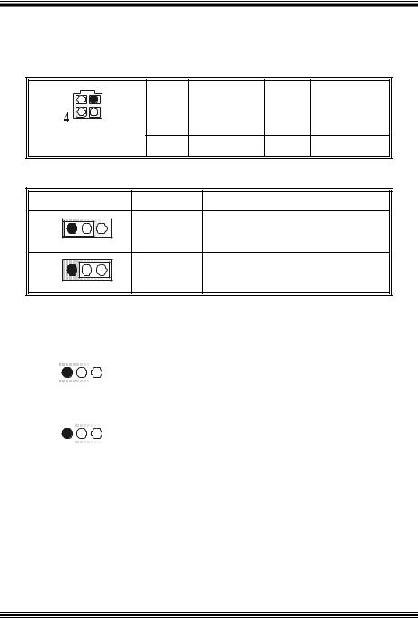
Clear CMOS Jumper: JCMOS1 |
|
|||||||||
|
|
|
|
|
|
|
|
|
|
|
|
|
|
|
|
JCMOS1 |
|
|
Assignment |
|
|
|
|
|
1 |
|
|
3 |
Pin 1-2 Close |
|
Normal Operation (default) |
|
|
|
|
|
|
|
|
|
|
|
|||||
|
|
|
|
|
|
|
|
|
|
||
|
1 |
|
|
3 |
Pin 2-3 Close |
|
Clear CMOS Data |
|
|
|
|
|
|
|
|
|
|
|
|||||
|
|
|
|
|
|
|
|
|
|
|
|
|
|
|
|
|
|
|
|
|
|
|
|
Clear CMOS Procedures:
1.Remov e AC power line.
2.Set the jumper to “Pin 1-2 Close”.
3.Wait for fiv e seconds.
4.Set the jumper to “Pin 2-3 Close”.
5.Power on the AC.
6.Reset y our desired password or clear the CMOS data.
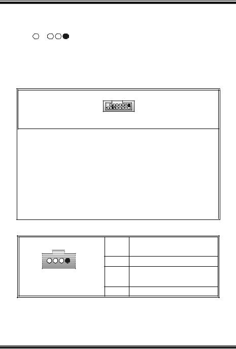
Case Open Connector: JCL1
|
|
Pin |
Assignment |
1 |
2 |
1 |
Case Open Signal |
|
JCL1 |
2 |
Ground |
|
|
Serial ATA Connector: JSATA1/ JSATA2
|
|
|
|
|
|
|
|
|
|
|
|
Pin |
Assignment |
Pin |
Assignment |
|
|
|
|
|
1 |
Ground |
2 |
TX+ |
|
|
|
|
|
|
|
|
|
|
|
|
|
|
|
|
|
|
|
|
|
|
|
|
|
|
|
|
|
|
|
|
|
|
|
|
|
|
10
6 5 3 2 |
|
|
|
|
4 |
TX- |
4 |
Ground |
||||
|
|
|
|
|
|
|
|
|
5 |
RX- |
6 |
RX+ |
7 4 1 |
|
|
|
|
7 |
Ground |
|
|
||||
JSATA1/ JSATA2
AUDIO DJ Connector: JDJ1
|
|
Pin |
Assignment |
Pin |
Assignment |
5 |
1 |
1 |
SMBDATA |
2 |
SMBCLK |
JDJ1 |
|
3 |
INT_B |
4 |
KEY |
|
|
5 |
ATX_PWROK |
|
|
Game Header: JGAME1
151
162
JGAME1
Pin |
Assignment |
Pin |
Assignment |
|
1 |
+5V |
2 |
+5V |
|
3 |
GP6 |
4 |
GP4 |
|
5 |
GP2 |
6 |
GP0 |
|
7 |
MIDI-OUTR |
8 |
Ground |
|
9 |
GP3 |
10 |
Ground |
|
11 |
GP7 |
12 |
GP1 |
|
13 |
MIDI-INR |
14 |
GP5 |
|
15 |
NA |
16 |
+5V |
|
CD-ROM Audio-In Header: JCDIN1/JCDIN2
|
Pin |
Assignment |
|
1 |
1 |
Left Channel Input |
|
2 |
Ground |
||
JCDIN1/2 |
3 |
Ground |
|
4 |
Right Channel Input |
||
|
11

Front Panel Audio Header: JAUDIO1
2 |
14 |
1 |
13 |
|
JAUDIO1 |
Pin |
Assignment |
Pin |
Assignment |
|
1 |
Mic In |
2 |
Ground |
|
3 |
Mic Power |
4 |
Audio Power |
|
5 |
RT Line Out |
6 |
RT Line Out |
|
7 |
Reserv ed |
8 |
Key |
|
9 |
LFT Line Out |
10 |
LFT Line Out |
|
11 |
RT Line In |
12 |
RT Line In |
|
13 |
LET Line In |
14 |
LET Line In |
|
Digital Audio Connector: JSPDIF_OUT1
|
Pin |
Assignment |
1 |
1 |
+5V |
JSPDIF_OUT1 |
2 |
SPDIF_OUT |
3 |
Ground |
Wake On LAN Header: JWO L1
|
Pin |
Assignment |
|
1 |
1 |
+5V_SB |
|
2 |
Ground |
||
JWOL1 |
|||
3 |
Wake up |
||
|
Front USB Header: JUSB2/3
|
|
Pin |
Assignment |
Pin |
Assignment |
|
2 |
10 1 |
+5V(f used) |
2 |
+5V(fused) |
||
1 |
9 |
3 |
USBP |
4 |
USBP |
|
5 |
USBP |
6 |
USBP |
|||
|
|
|||||
JUSB2/3 |
|
7 |
Ground |
8 |
Ground |
|
|
|
9 |
KEY |
10 |
NC |
|
12

Back Panel Connectors
Mouse |
|
|
Parallel |
LAN |
|
|
|
|
Line In/ Surround |
||
|
|
|
|
|
|
|
|
1 |
3 |
|
Speaker Out |
|
|
1 |
3 |
|
Mic In/ Bass&Center |
Keyboard |
USB |
COM1 |
|
USB |
|
JKBMS1 |
JUSB1 |
JCOM1 |
JVGA1 |
JRJ45USB1 |
JAUDIO |
13

Español
Características del P4TSV
A. Hardware
CPU
 Proporciona Socket-478.
 Soporta procesador Intel Pentium 4 de hasta 3.06GHz.
 Front Side Bus a 400/533/800MHz.
 Soporta Hyper-Threading.
 Soporta Northwood y Prescott CPU. (No soporta CPU Willamette)
Chipset
 North Bridge: Intel 865G
 South Bridge: Intel ICH5.
Memoria Principal
 Soporta una o dos DDR canal de datos de 64-bit wide con 1 o 2 DIMMs por canal.
 Banda ancha disponible hasta 3.2GB/s (DDR400) para modo de canal simple y modo de canal doble 6.4GB/s (DDR 400).
 Soporta tecnologia DDR de 128-MB, 256-Mb, 512-Mb y 1 GB.
 Soporta solamente dispositivos DDR x8, x16.( No soporta DIMMs registered o
DIMMs de doble cara X 16)
 Soporta dispositivos de 4 bancos.
  Tamaño de memoria máxima 4GB.
Super I/O
 Chip: ITE IT8712F.
 Interf ace Low Pin Count.
 Proporciona f uncionalidad legacy Super I/O.
 Env ironment Control initiatives,
-H/W Monitor
-Controlador Fan Speed
-Función ITE "Smart Guardian"
Ranuras
 Tres ranuras de 32-bit PCI bus master.
 Una ranura CNR.
 Una ranura AGP 4X/ 8X.
IDE Onboard
 Soporta cuatro discos IDE.
 Soporta modo PIO 5, modo Bride y Ultra DMA 33/66/100 Bus Modo Master.
 Soporta 2 puertos Serial ATA (SATA).
- Conf orma con la especificación SATA 1.0
14

- Transf erencia de datos de hasta 1.5 GB/s
LAN
 Chip: RTL8100B.
 Soporta 10 Mb/s y 100 Mb/ auto-negociación
 Capacidad Half/ Full duplex.
 Soporta administración ACPI
AC’97 Sound Codec Onboard
 Chip: CMI9739A.
 Conf orma con la especificación AC’97.
 Interf ace AC97 2.2.
 Soports 6 canales.
Periféricos Onboard
a.ParteTrasera
 1 puerto serie.
 1 puerto paralelo. (modo SPP/EPP/ECP)
 1 puerto VGA.
 Puerto de Audio v ertical.
 1 LAN RJ-45.
 Soporta ratón PS/2y teclado PS/2.
  4 puertos USB2.0.
b.ParteFrontal
 1 puerto para disquetera soporta 2 FDDs con 360K, 720K, 1.2M, 1.44M y 2.88 Mby tes.
 4 puertos USB2.0.
Dimensiones
 Forma de Factor Micro ATX: 24.4 X 24.4cm (W X L)
B. BIOS & Software
BIOS
 Award legal BIOS.
 Soporta APM1.2.
 Soporta ACPI.
 Soporta f unción USB.
Software
 Soporta Warpspeeder™, 9th Touch™, FLASHER™, StudioFun!™ (opcional).
 Of rece el más alto funcionamiento para Windows 98 SE, Windows 2000, Windows Me, Windows XP, SCO UNIX etc.
15
Contenido del Paquete
 Cable HDD X 2
 Cable FDD X1
 Manual del Usuario X1
 Conf iguración Completa del Driv er CD X1
 Aplicación StudioFun! CD X 1 (opcional)
 Cable USB 2.0 X1 (opcional)
 Cable S/PDIF X 1 (opcional)
 Panel Trasero I/O para carcasa Micro ATX X1 (opcional)
 Cable Serial ATA X1
 Cable de Interruptor de Corriente para Serial ATA X1
Cómo instalar un Puente
La ilustración muestra cómo instalar un puente. Cuando el Jumper Cap está ubicado en los contactos, el puente está en “close”. Si no hay Jumper Cap ubicado en los contactos,
el puente está en ”open”. La siguiente ilustración muestra un contacto 3 en el que los contactos 1y 2 están “close” cuando el Jumper Cap está ubicado en los dos contactos.
|
|
|
|
|
Puente open |
Puente close |
Contacto 1-2 close |
||
Instalación del CPU
Paso 1: Empuje la palanca hacia afuera del socket y levante la palanca hasta un ángulo de 90 grados.
Paso 2: Fíjese por el punto blanco o márgen cortado. El punto blanco o márgen cortado
debería apuntar hacia el piv ote de la palanca. La CPU solamente se f ijará en una sola correcta orientación.
Paso 3: Tome el CPU f irmemente hacia abajo, y cierre la palanca para completar la instalación.
Paso 4: Ponga el ventilador de la CPU en el CPU y asegúrelo. Conecte el cable de
16

corriente del v entilador de la CPU al JCFAN1. Ésto completa la instalación.
paso1 |
paso 2 |
paso 3 |
paso4 |
Cabezal del Sistema de Ventilación del CPU: JCFAN1
1 |
Contacto |
Asignación |
|
|
1 |
Tierra |
|
JCFAN1 |
2 |
+12V |
|
3 |
FAN RPM Sense |
||
|
Cabezal del Sistema de Ventilación: JSFAN1
1 |
JSFAN1 |
Contacto |
Asignación |
1 |
Tierra |
2 |
+12V |
3 |
FAN RPM Sense |
|
|
Módulos DDR DIMM: DDRA1-2, DDRB1-2
 Soporta hasta cuatro DDR DIMMs (dos DIMMs por canal), doble o/y una cara.
 Para manejarse con el Dual Channel, los DIMMs deben ser insertados en pares idénticos. Debe ser la combinaciٛ n del DDRA1+DDRB1 (DIMMs azules)
o DDRA2+DDRB2 (DIMMs blancos). Para más inf ormación sobre la operación del Dual Channel por f avor entre a la página web: www.biostar.com.tw)
DRAM Tiempo de Acceso: 2.5V Unbuffered/ no registered (sin ECC) DDR SDRAM PC2100/ PC2700/ PC3200 Tipo requerido.
DRAM Tipo: 128MB/ 256MB/ 512MB/ 1GB Módulo DIMM (184 contactos)
Total del Tamaño de la Memoria con Unbuffered/ Registered DIMMs
17

|
|
|
|
|
|
Localización del |
Módulo DDR |
Total del |
|
|
Socket DIMM |
|
Tamaño de la |
|
|
|
|
Memoria |
|
|
|
|
(MB) |
|
|
DDRA1 |
64MB/128MB/256MB/512MB/1GB |
|
|
|
|
*1 |
|
|
|
DDRA2 |
64MB/128MB/256MB/512MB/1GB |
|
|
|
|
*1 |
Máxima |
|
|
DDRB1 |
64MB/128MB/256MB/512MB/1GB |
4GB |
|
|
|
*1 |
|
|
|
DDRB2 |
64MB/128MB/256MB/512MB/1GB |
|
|
|
|
*1 |
|
|
|
|
|
|
|
|
|
***Solamente para referencia*** |
|
|
Instalación del Módulo DDR
1.Abra una ranura de DIMM presionando el clip de retención hacia af uera. Aliñe el DIMM en la ranura tales que la muesca en el DIMM encaje en la cumbrera de la ranura.
2.Inserte el DIMM v erticalmente y firmemente en
la ranura hasta que el clip de retención v uelva a su posición original y el DIMM esté correctamente colocado.
18
Puentes, Cabezales, Conectores y Ranuras
Conector de Disquetera: FDD1
La placa madre proporciona un conector estándar para disquete que soporta disquetera de 360K, 720K, 1.2M, 1.44M y 2.88M. Éste conector utiliza cables
proporcionados por el disquete.
Conector del Disco Duro: IDE1/ IDE2
La placa madre tiene un controlador de 32-bit PCI IDE que proporciona Modo PIO 0~5, Bus Master, y funcionalidad Ultra DMA 33/ 66/ 100. Tiene dos conectores
HDD: IDE1 (primario) y IDE2 (secundario).
Los conectores IDE puede conectar a un disco master y uno esclavo, así puede conectar hasta cuatro discos duros. El primer disco duro debe estar siempre conectado al IDE1.
Ranuras de Interconexión del Componente Periférico: PCI1-3
Ésta placa madre está equipada con 3 ranuras estándar PCI. PCI es la sigla para Interconexión del Componente Perif érico, y es un bus estándar para tarjetas de expansión. Ésta ranura PCI está diseñado con 32 bits.
Ranura del Puerto Acelerado para Gráficos: AGP1
Su monitor se f ijará directamente a la tarjeta de video. Ésta placa madre soporta tarjetas de v ideo para ranuras PCI, pero también está equipado con un puerto
AGP. La tarjeta AGP tomará v entaja de la tecnología del AGP para el mejoramiento de la eficiencia y funcionamiento del video, especialmente con
gráf icos 3D.
Ranura de Banda de Suspensión de Comunicación y Red: CNR1
La especificación CNR es una abierta Industria de Arquitectura Estándar, que def ine una tarjeta de interf ace escalable del hardware en el que soporta solamente modem.
ConectorSerial ATA: JSATA1/JSATA2
La placa madre tiene un controlador PCI al SATA con 2 canales SATA |
de |
interf ace, que satisf ace SATA 1.0 spec y transf iere datos a una v elocidad |
de |
1.5GHz. |
|
19

Conector del Panel Frontal: JPANEL1
SLP |
PWR_LED ON/OFF |
IR |
JPANEL1 |
2 |
24 |
|
1 |
2 3 |
||
|
|
|
|
|
SPK |
HLED |
RST |
IR |
|
|
|
|
|
|
|
|
|
|
||||||
|
|
|
|
|
|
||||||
Con- |
Asignación |
Función |
Con- |
Asignación |
Función |
||||||
tactos |
|
|
|
tactos |
|
|
|
|
|
||
1 |
+5V |
|
|
2 |
Control de |
|
Botón |
||||
|
|
|
|
Conector |
|
Suspension |
|
de Suspension |
|||
3 |
NA |
del Altav oz |
4 |
Tierra |
|
|
|
|
|||
5 |
NA |
|
|
6 |
NA |
|
NA |
||||
7 |
Altav oz |
|
|
8 |
Corriente LED (+) |
Corriente |
|||||
9 |
HDD LED (+) |
|
LED |
10 |
Corriente LED (+) |
LED |
|||||
11 |
HDD LED (-) |
del Disco Duro |
12 |
Corriente LED (-) |
|
|
|
||||
13 |
Tierra |
Botón |
14 |
Botón de |
|
Botón de |
|||||
|
|
|
|
de Reinicio |
|
Encendido |
|
Encendido |
|||
15 |
Control de |
|
|
16 |
Tierra |
|
|
|
|
||
|
|
|
Reinicio |
|
|
|
|
|
|
|
|
17 |
NA |
|
|
18 |
KEY |
|
|
|
|
||
19 |
NA |
|
|
20 |
KEY |
|
|
|
|
||
21 |
+5V |
Conector IrDA |
22 |
Tierra |
|
Conector IrDA |
|||||
23 |
IRTX |
|
|
24 |
IRRX |
|
|
|
|
||
|
|
Conectores de Corriente: JATXPWER1/ JATXPWR2 |
|
||||||||
|
|
|
|
|
|
|
|
|
|
|
|
|
|
|
|
Con- |
Asignación |
Con- |
Asignación |
||||
10 |
2 0 |
tactos |
+3.3V |
tactos |
+3.3V |
|
|
|
1 |
11 |
|||
|
|
2 |
+3.3V |
12 |
-12V |
|
|
|
3 |
Tierra |
13 |
Tierra |
|
|
|
4 |
+5V |
14 |
PS_ON |
|
|
|
5 |
Tierra |
15 |
Tierra |
|
1 |
11 |
6 |
+5V |
16 |
Tierra |
|
7 |
Tierra |
17 |
Tierra |
|||
|
|
20
|
|
|
|
|
|
|
|
JATXPWR1 |
8 |
PW_OK |
18 |
-5V |
|
|
|
9 |
+5V_SB |
19 |
+5V |
|
|
|
10 |
+12V |
20 |
+5V |
|
|
|
|
|
|
|
|
2 |
1 |
Con- |
Asignación |
Con- |
Asignación |
|
3 |
tactos |
+12V |
tactos |
Tierra |
|
1 |
3 |
|||
JATXPWR2 |
2 |
+12V |
4 |
Tierra |
|
|
|
||||
5V / 5VSBSelección para KB: JKBV1
JKBV1 |
|
Asignación |
Descrición |
|
1 |
3 |
+5V |
5V para teclado y ratón |
|
Contacto 1-2 close |
|
|||
|
|
|||
1 |
3 |
+5V_SB |
5V standby de teclado y ratón para |
|
Contacto 2-3 close |
encender su sistema |
|||
|
||||
5V/ 5VSBSelección para USB: JUSBV1/ JUSBV2/JUSBV3_4
|
|
|
|
|
|
|
|
|
JUSBV1/JUSBV2/ |
Asignación |
Description |
|
|||
|
JUSBV3_4 |
|
|
|
|
||
|
1 |
|
|
3 |
+5V |
5V JUSBV1 para puerto JUSB1 |
|
|
|
|
|
||||
|
|
|
|
|
|
5V JUSBV2 para puerto JRJ45USB1 |
|
|
Contacto 1-2 close |
|
|
||||
|
|
5V JUSBV3_4 para puerto JUSB2/3 |
|
||||
|
|
|
|
|
|
|
|
|
1 |
|
|
3 |
+5V_SB |
JUSBV1 5V standby para encender el |
|
|
|
|
|
||||
|
|
|
|
|
|
puerto JUSB1 |
|
|
|
|
|
|
|
|
|
|
Contacto 2-3 close |
|
|
||||
|
|
JUSBV2 5V standby para encender el |
|
||||
|
|
|
|
|
|
|
|
|
|
|
|
|
|
puerto JRJ45USB1 |
|
|
|
|
|
|
|
JUSBV3_4 5V standby para encender |
|
|
|
|
|
|
|
los puertos JUSB2/3 |
|
|
|
|
|
|
|
|
|
21

Borrar Puente CMOS: JCMOS1
|
JCMOS1 |
Asignación |
|
1 |
3 |
Pin 1-2 Close |
Operación Normal (default) |
|
|
|
|
1 |
3 |
Pin 2-3 Close |
Borra datos CMOS |
|
|
|
|
Procedimientos para Borrar CMOS:
1.Quite el cable de corriente del AC.
2.Fijar el puente en el “contacto 2-3 close”.
3.Espere 5 segundos.
4.Fijar el Puente en el “contacto 1-2 close”.
5.Encienda AC.
6.Reconf igure la contraseña deseada o borre datos CMOS.
Conector de la Carcasa Abierta: JCL1
|
|
|
Con- |
Asignación |
1 |
|
2 |
tactos |
|
|
1 |
Señal de la Carcasa Abierta |
||
|
|
|
|
|
|
JCL1 |
|
2 |
Tierra |
|
|
|
|
ConectorSerial ATA: JSATA1/ JSATA2
|
|
|
|
|
|
|
|
|
|
|
|
|
|
|
|
|
|
|
|
|
Con- |
|
Con- |
|
|
|
6 5 3 2 |
|
|
|
tac- |
Asignación |
tac- |
Asignación |
|
|||
|
|
|
|
tos |
|
|||||||
|
|
|
|
|
|
|
|
tos |
|
|
|
|
|
|
|
|
|
|
|
|
|
|
|
||
|
|
|
|
|
|
|
|
|
|
|
|
|
|
|
|
|
|
|
|
|
1 |
Tierra |
2 |
TX+ |
|
|
|
7 4 1 |
|
|
|
|
||||||
|
JSATA1/ JSATA2 |
4 |
TX- |
4 |
Tierra |
|
||||||
|
|
|
|
|
|
|
|
5 |
RX- |
6 |
RX+ |
|
|
|
|
|
|
|
|
|
7 |
Tierra |
|
|
|
|
|
|
|
|
|
|
|
|
|
|
|
|
22
Conector Audio DJ: JDJ1
|
|
|
|
|
|
|
|
|
|
|
|
|
Con- |
Asignación |
Con- |
Asignación |
|
|
5 |
|
1 |
tactos |
tactos |
|
||
|
|
|
|
|
||||
|
|
|
|
|||||
|
|
|
|
1 |
SMBDATA |
2 |
SMBCLK |
|
|
|
JDJ1 |
|
|
||||
|
|
|
3 |
INT_B |
4 |
KEY |
|
|
|
|
|
|
|
||||
|
|
|
|
5 |
ATX_PWROK |
|
|
|
|
|
|
|
|
|
|
|
|
Cabezal de Juego: JGAME1
151
162
JGAME1
Contactos |
Asignación |
Contactos |
Asignación |
|
1 |
+5V |
2 |
+5V |
|
3 |
GP6 |
4 |
GP4 |
|
5 |
GP2 |
6 |
GP0 |
|
7 |
MIDI-OUTR |
8 |
Tierra |
|
9 |
GP3 |
10 |
Tierra |
|
11 |
GP7 |
12 |
GP1 |
|
13 |
MIDI-INR |
14 |
GP5 |
|
15 |
NA |
16 |
+5V |
|
Cabezal de Entrada de Audio CD-ROM: JCDIN1/ JCDIN2
|
Contac- |
Asignación |
|
1 |
tos |
|
|
1 |
Entrada del Canal Izquierdo |
||
JCDIN1/ 2 |
2 |
Tierra |
|
3 |
Tierra |
||
|
|||
|
4 |
Entrada del Canal Derecho |
23
 Loading...