


P4TDP
FCC Statement and Copyright
This equipment has been tested and f ound to comply with the limits of a Class B digital device, pursuant to Part 15 of the FCC Rules. These limits
are designed to provide reasonable protection against harmful interf erence in a residential installation. This equipment generates, uses and can
radiate radio frequency energy and, if not installed and used in
accordance with the instructions, may cause harmf ul interference to radio communications. There is no guarantee that interference will not occur in a
particular installation.
The v endor makes no representations or warranties with respect to the contents here of and specially disclaims any mplied warranties of merchantability or fitness for any purpose. Further the v endor reserv es the right to rev ise this publication and to make changes to the contents here of without obligation to notify any party beforehand.
Duplication of this publication, in part or in whole is not allowed without first obtaining the v endor’s approval in writing.
The content of this user’s is subject to be changed without notice and we will not be responsible f or any mistakes found in this user’s manual. All the brand and product names are trademarks of their respective companies.
i

Contents |
|
ENGLISH............................................................................................. |
1 |
P4TDP Features............................................................................................................................... |
1 |
Package contents ........................................................................................................................... |
2 |
Layout of P4TDP ............................................................................................................................. |
2 |
CPU Installation ............................................................................................................................... |
3 |
DDR DIMM Modules: DDR1-2....................................................................................................... |
4 |
Jumpers, Head ers, Connectors & Slots ................................................................................... |
5 |
ESPAÑOL.......................................................................................... |
10 |
Características del P4TDP.......................................................................................................... |
10 |
Contenido del Paqu ete................................................................................................................ |
11 |
Disposición del P4TDP................................................................................................................ |
11 |
Instalación de la CPU................................................................................................................... |
12 |
Módulos DDR DIMM: DDR1-2.................................................................................................... |
13 |
Puentes, Cabez ales, Conectores y Ranuras ......................................................................... |
14 |
WARPSPEEDER................................................................................ |
19 |
Introduction.................................................................................................................................... |
19 |
System Requirement ................................................................................................................... |
20 |
Installation ...................................................................................................................................... |
20 |
Usage ............................................................................................................................................... |
22 |
TROUBLE SHOOTING ....................................................................... |
30 |
SOLUCIÓN DE PROBLEMAS............................................................. |
31 |
ii

English
P4TDP Features
Use Intel 845D/ ICH2 Chipset, ITE IT8712.
Contains on board I/O facilities, which include two serial port, a parallel port, a PS/2 mouse port, a PS/2 key board port, audio ports, USB ports, a game port .
Supports the Intel Pentium 4® (Socket 478) processor up to 2.4GHz.
Supports Ultra 100/66/33, BMIDE and PIO modes.
Supports up to 2 DDR 200/266/Fuzzy 333 MHz dev ices, running at 400 MHz/ Fuzzy 533 Front Side Bus frequency.
Supports fiv e 32-bit PCI Bus slots, and one CNR Slot (Ty pe A only ) .
(If the function CODEC is onboard, then the CNR slot only support slave card. But if the H/W Audio is onboard, then the CNR slot support only primary card . )
Supports USB1.1.
Supports USB2.0(optional).
Complies with PC ATX f orm f actor specif ications.
Supports popular operating systems such as Windows 98, Windows NT, Windows 2000, Windows ME, Windows XP, LINUX and SCO UNIX.
DIMM Power Selection by BIOS setup to adjust DDR DIMM voltage. (If y ou
meet the DDR DIMM compatible program, try to adjust the DDR Voltage to fix the compatible program.)
Intel® AC’97 2.2 compatible.
High S/N ratio meets PC 99 requirements.
6CH , applicable for leading motherboard chipsets.
Line-in phone-jack share with rear out .
Mic-in phone-jack share with Bass and Center.
1
Package contents
HDD Cable X 1, FDD Cable X 1, Fully Setup Driv er CD X 1
USB Cable X 2 (Optional)
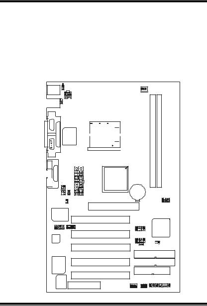
Layout of P4TDP
JKBMS1 |
JK BV 1 |
K/B |
& |
|
Mouse |
JATXP WR2 |
JUS B1 |
|
|
JUS BV1 |
|
JCOM1 |
|
1 |
Port |
|
COM |
|
|
|
JP RNT1 |
|
|
Parallel |
I/ O |
|
|
|
|
JCOM2 |
|

 t478 Socke


UT |
JGAME1 |
|
SP-O |
ort |
|
IN-MICLINE-IN |
GAMEP |
INTEL 845D |
|
|
|
|
2 |
|
|
JUS B4 |
JATXP WR1 |
|
JUS BV 4 |
|
|
|
|
|
J1 |
A GP1 |
US B 2.0 |
|
Chi p |
P CI1 |
(o pt ion al) |
|
JAU DI O1 |
JCD IN 1 |
2 |
|
1 |
P CI2 |
|
|
Co de c |
|
(o ption al) |
P CI3 |
|
|
|
P CI4 |
H/ W
AUD IO
Chi p
(o pti on al) |
P CI5 |
JCFAN 1
1 |
DDR 2
DDR 1
BAT1
JD IM MVOLT1
2 |
1 |
|
JU SB 3 |
2 |
INTEL ICH2 |
2 |
JU SB 2 |
JCMOS 1 |
|
||
|
1 |
|
|
JUSBV2_3 |
IDE1 |
|
|
PR IMA RY ID E CON N.
SEC ONDAR YIDE CONN.
FL OPPY DISK C ONN. IDE2
BIO S
CNR 1
FD D1
JS FA N1 JWO L1 |
JPAN EL1 |
||
1 |
1 |
2 |
2 4 |
|
|
1 |
2 3 |
2
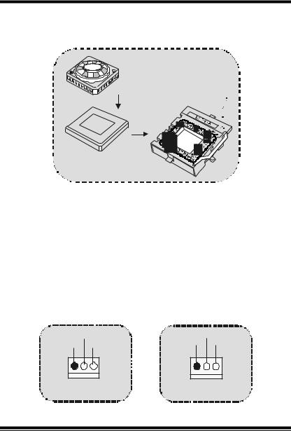
CPU Installation
CPU
1.Pull the lever sideways away f rom the socket then raise the lever up to 90-degree angle.
2. Locate Pin A in the socket and lock f or the white dot or cut edge in the CPU. Match Pin A with the white dot/cut edge then insert the
CPU.
3. Press the lever down. Then Put the f an on the CPU and buckle it and put the f an’s power port into the JCFAN1, then to complete the installation.
CPU/ System Fan Headers: JCFAN1/ JSFAN1
12V |
12V |
Ground Sense |
Ground Sense |
1 |
1 |
JCFAN1 |
JSFAN1 |
3
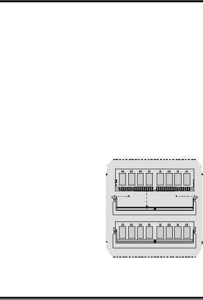
DDR DIMM Modules: DDR1-2
DRAM Access Time: 2.5V Unbuffered DDR 200/266 MHz Ty pe
required x16 not support .
DRAM Ty pe: 64MB/ 128MB/ 256MB/ 512MB/ 1GB DIMM Module (184 pin)
|
|
|
|
|
|
DIMM Socket |
DDR Module |
Total Memory |
|
|
Location |
|
Size (MB) |
|
|
DDR 1 |
64MB/128MB/256MB/512MB/1GB |
Max is |
|
|
|
*1 |
|
|
|
DDR 2 |
64MB/128MB/256MB/512MB/1GB |
2GB |
|
|
|
*1 |
|
|
|
|
|
|
|
* The list shown above f or DRAM configuration is only f or ref erence.
How to install a DIMM Module
1. The DIMM socket has a “ Plastic Safety Tab”, and the DIMM memory module has an
“Asymmetrical notch”, so the DIMM memory module can only
fit into the slot in one direction.
2. Push the tabs out. Insert the DIMM memory modules into the socket at a 90-degree angle, then
push down v ertically so that it will fit into the place.
3. The Mounting Holes and plastic tabs should f it over the edge and
hold the DIMM memory modules in place.
4

Jumpers, Headers, Connectors & Slots
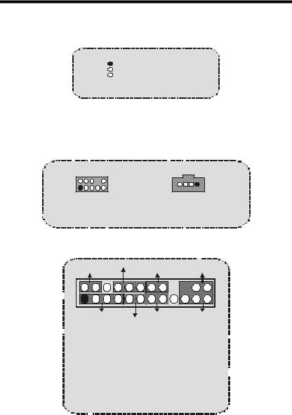
Hard Disk Connectors: IDE1/ IDE2
The motherboard has a 32-bit Enhanced PCI IDE Controller that provides PIO Mode 0~4, Bus Master, and Ultra DMA / 33/ 66/ 100 f unctionality. It has two HDD connectors IDE1 (primary ) and IDE2
(secondary ).
The IDE connectors can connect a master and a slav e drive, so you can connect up to four hard disk driv es. The f irst hard driv e should alway s be connected to IDE1.
Floppy Disk Connector: FDD1
The motherboard prov ides a standard f loppy disk connector that
supports 360K, 720K, 1.2M, 1.44M and 2.88M f loppy disk ty pes. This connector supports the prov ided f loppy drive ribbon cables.
Communication Network RiserSlot: CNR1
The CNR specif ication is an open Industry Standard Architecture, and it def ines a hardware scalable riser card interf ace, which supports audio,
network and modem only (slave card only) .
(If the function CODEC is onboard, then the CNR slot only support slave card. But if the H/W Audio is onboard, then the CNR slot support only primary card . )
Accelerated Graphics Port Slot: AGP1
Unlike the mouse ports, key board ports and printer ports this motherboard does not hav e built in v ideo facilities and therefore requires a video card f or one of the expansion slots. Your monitor will attach directly to that v ideo card. This motherboard supports video cards f or PCI and ISA slots but is also equipped with an Accelerated Graphics Port (AGP). An AGP card will take advantage of AGP technology f or improv ed video efficiency and perf ormance, especially with 3D graphics.
Peripheral Component Interconnect Slots: PCI1-5
This motherboard is equipped with 5 standard PCI slots. PCI stands f or Peripheral Component Interconnect, and it is a bus standard f or expansion cards, which has, supplanted the older ISA bus standard in most ports. This PCI slot is designated as 32 bits.
5
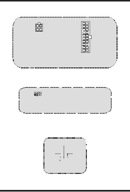
Power Connectors: JATXPWR1/ JATXPWR2
JATXPWR2
(ATX 12V Power Conn.)
JATXPWR1
(ATX Main Power Conn.)
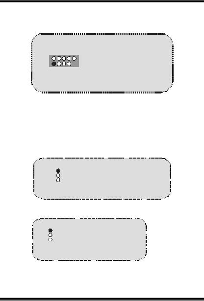
DIMM Power Selection Connector: JDIMMVOLT1
(Optional)
2 1
1
JDIMMVOLT
(Default ==> 2.5V)
Jump Open==> 2.5V Pin 1-2 on ==> 2.6V
Pin 3-4 on ==> 2.7V Pin 5-6 on ==> 2.8V Pin 7-8 on ==> 2.9V
zIt strongly recommended to set DDR DIMM voltage in def ault setting 2.5V, and it f or over v oltage function.
Wake On LAN Header: JWO L1
Ground
5V_SB Wake up
1 

WOL1
6
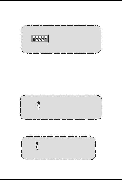
Front USB Header: JUSB2/ JUSB3(Optional)
/ JUSB4(Optional)
|
Pin1,2 |
==> +5V |
2 |
Pin3,4 |
==> Data(-) |
Pin5,6 |
==> Data(+) |
|
1 |
Pin7,8 |
==> Ground |
JUSB2/3/4 |
Pin9 |
==> KEY |
|
Pin10 |
==> NA |
zBasically JUSB1/2 supports USB1.1, but after adding an USB2.0 chip, JUSB1/4(white) supports USB2.0.
zHaving an USB2.0 chip, JUSB1/4(white) supports USB2.0 and JUSB2/3 only supports USB1.1.
5V/ 5VSB Selection for USB: JUSBV1/2_3
|
|
|
|
|
|
|
|
|
/ JUSBV4(Optional) |
|||||
|
|
|
|
|
|
|
|
|
|
|
|
|
|
|
1 |
|
|
|
|
Pin 1-2 on ==> 5V |
|||||||||
|
|
|
||||||||||||
|
|
|
|
_3/4 Pin 2-3 on ==> 5V_SB |
||||||||||
JUSBV1/2 |
|
|||||||||||||
|
|
|
|
|
|
|
|
|
||||||
5V/ 5VSB Selection for KB: JKBV1 |
||||||||||||||
1 |
|
|
|
|
Pin 1-2 on ==> 5V |
|||||||||
|
|
|
|
|||||||||||
|
|
|
|
|
|
|
Pin 2-3 on ==> 5V_SB |
|||||||
|
|
JKBV1 |
||||||||||||
|
|
|
|
|
|
|
|
|
|
|||||
7
5V/ 5VSB Selection for USB WAKE-UP: J1(Optional)
1 |
|
Pin 1-2 ==> on |
|
|
Pin 2-3 ==> off |
|
J1 |
zWhen VT6202 support 5V/5VSB Selection for USB WAKE-UP in on mode, JUSB1 and JUSB4 will change to 5V_SB
Audio Subsystem: JAUDIO1/ JCDIN1
2 |
1 |
1 |
|
JAUDIO1 |
JCDIN1 |
(Front Audio Header) (CD-ROM Audio-In Header)
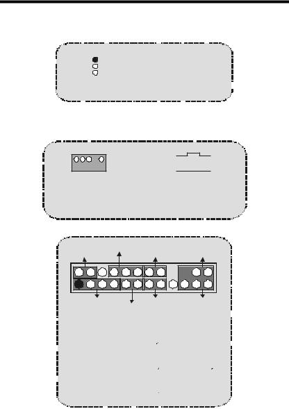
Front Panel Connector: JPANEL1
SLP |
PWR_LED |
ON/O FF |
IR |
||
( +) |
(+) |
(-) |
|||
2 |
|
|
|
|
24 |
1 |
|
|
|
|
23 |
SPK |
|
(+) |
(-) |
RST |
IR |
|
HLED |
||||
|
SPK |
==> Speaker Conn. |
||||
|
||||||
|
||||||
|
HLED |
==> Hard Driver LED |
||||
|
RST |
==> Reset Button |
||||
|
IR |
==> Infrared Conn. |
||||
|
SLP |
==> Sleep Button |
|
|
||
|
|
|||||
|
PWR_LED ==> Power LED |
|||||
|
ON/ OFF |
==> Power-on Button |
||||
|
|
|
|
|
|
|
|
|
|
|
|
|
|
|
|
|
|
|
|
|
|
|
|
|
|
|
|
8

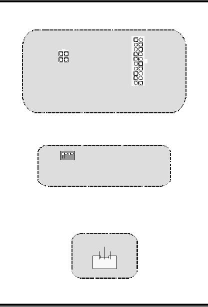
Clear CMOS Jumper: JCMOS1
|
|
|
|
|
|
|
1 |
Pin 1-2 on ==> Normal Operation |
|||
|
|||||
|
|
|
|
(default) |
|
|
|
|
|
||
 JCMOS1 Pin 2-3 on ==> Clear CMOS Data
Back Panel Connectors
JKBMS1 |
|
|
|
JPRNT1 |
JGAME1 |
|||||||||||||||||||
PS/2 |
|
|
|
|||||||||||||||||||||
M ouse |
|
|
|
|
|
|
|
|
|
|
|
|
|
|
|
|
Game P ort |
|||||||
|
|
|
|
|
|
|
|
|
|
|
|
|
|
|
|
|
||||||||
|
|
|
|
|
|
|
|
|
|
|
|
|
|
|
|
|
|
|
|
|
|
|
|
|
|
|
|
|
|
|
|
|
|
|
|
|
|
|
|
|
|
|
|
|
|
|
|
|
|
|
|
|
|
|
|
|
|
|
|
|
|
|
|
|
|
|
|
|
|
|
|
|
|
|
P S/2 |
USB |
COM11 |
|
Mic |
Keyboard |
|
JCOM1 |
JCOM2 |
In |
|
|
|
4 Channel Spe akers |
6 Channel Speakers |
|||
Speaker Out |
Line In/ |
Mic In |
Speaker Out Line In/ |
Mic In/ Center & Bass |
|
Rear Speaker |
|
Rear Speaker |
|
9

Español
Características del P4TDP
Usa Chipset Intel 845D/ ICH2, ITE IT8712.
Contiene f acilidades I/O integrados en la |
placa madre en el que incluy e |
dos puertos en serie, un puerto paralelo, |
un puerto para ratón PS/2, un |
puerto para teclado PS/2, puertos de audio, puertos USB y un puerto de juego .
Soporta procesadores Intel Pentium 4® (Socket 478) de hasta 2.4GHz.
Soporta Ultra 100/66/33, BMIDE y modos PIO.
Soporta hasta 2 dispositivos DDR 200/266/Fuzzy 333 MHz, corriendo a 400 MHz/ Fuzzy 533 MHz f recuencia Front Side Bus.
Soporta cinco ranuras PCI 32-bit y una ranura CNR (solamente de Tipo
A).
(Si la función CODEC está integrado en la placa madre, entonces la ranura CNR solamente puede soportar tarjeta esclava. Pero si el
Audio H/W está integrado en la placa madre, entonces la ranura CNR solamente puede soportar tarjeta primaria.)
Soporta USB1.1.
Soporta USB2.0 (opcional).
Compatible con las especificaciones del factor de forma de tamaño de PC ATX.
Soporta sistemas operativ os populares tales como Windows 98, Windows NT, Windows 2000, Windows ME, Windows XP, LINUX y SCO UNIX.
Corriente de Selección DIMM para configuración BIOS utilizado para ajustar voltaje DDR DIMM. (Si se encuentra con un programa compatible al DDR DIMM, trate de ajustar el v oltaje DDR para fijar con el programa compatible.)
Compatible con Intel® AC’97 2.2.
Alto S/N ratio para requerimientos PC 99.
10

6CH , aplicable para chipsets de principales placas madres.
Entrada de Línea phone-jack compartido con el rear out. Micróf ono phone-jack compartido con Bassy Center.
Contenido del Paquete
Cable HDD X 1, Cable FDD X 1, Conf iguración Completa del Driv er CD X 1
Cable USB X 2 (Opcional)
Disposición del P4TDP
JKBM S1 |
|
Teclado |
JKBV1 |
& |
JATXPWR 2 |
R aton |
|
JUSB 1 |
|
|
JUSB V1 |
COM1 |
JC OM1 |
|
|
aralelo |
J PRNT1 |
||
|
P |
|
I/O |
|
Puerto |
|
|
|
|
|
|
|
JC OM2 |
|
|
d el oz |
J GAME 1 |
|
En tra da Salida de Lin ea Altav |
rto de Jue go |
|
Entrada delM IC |
2 |
|
Pue |
|
|
J USB 4 |
J ATXPW R1 |
|
|
JUSBV4 |
|
|
|
|
|
J1 |
AGP1 |
|
USB 2.0 |
|
|
Chip |
|
(opcional ) |
|
|
J AUDIO1 |
J C DIN1 |
|
2 |
|
|
1 |
|
|
Co dec (opci ona l)
AUDI O
H/W
Chi p (opcio nal)
8 47 et ck So
INTEL 845D
JC FAN1
1 |
DDR 2
DD R 1
BAT1
J DIMM VOLT1
2 |
1 |
PC I1 |
|
J U SB 3 |
|
|
|
||
|
|
||
PC I2 |
2 |
|
INTEL ICH2 |
|
|
|
|
|
|
|
|
|
J USB 2 |
J CMOS 1 |
PC I3 |
2 |
|
1 |
|
|
|
|
|
|
J USBV2-3 |
IDE1 |
|
|
|
PC I4 |
CON ECTOR I DE PRI MARI O |
|
|
|
|
|
CO N ECT OR ID ES ECU N DA R IO |
|
PCI5 |
|
ID E2 |
Con ect or para Di squ ete |
||
|
|
|
|
FDD1 |
|
BIOS |
J SFAN1 J WOL 1 |
J PANE L1 |
|
||
C NR1 |
1 |
1 |
2 |
|
24 |
|
|
1 |
|
23 |
|
11

Instalación de la CPU
CPU
1. Tire de la palanca del lado del zócalo, luego lev ante la palanca hasta un ángulo de 90 grados.
2.Sitúe el contacto A del zócalo y busque el punto blanco o corte el borde en la CPU. Empareje el contacto A con el punto blanco/ corte del borde, luego inserte la CPU.
3.Presione la palanca para abajo. Ponga el v entilador en la CPU y abróchelo. Luego ponga el puerto de corriente del ventilador en el JCFAN1. Y y a habrá completado su instalación.
CPU/ Cabezales del Sistema de Ventilación: JCFAN1/ JSFAN1
12V |
12V |
Tierra Sense |
Tierra Sense |
1 |
1 |
JCFAN1 |
JSFAN1 |
12

Módulos DDR DIMM: DDR1-2
DRAM Tiempo de Acceso: 2.5V Unbuffered DDR 200/266 MHz no
soporta Tipo requerido x16.
DRAM Tipo: 64MB/ 128MB/ 256MB/ 512MB/ 1GB Módulos DIMM (184 contactos)
|
|
|
|
|
|
Localización |
Módulo DDR |
Total del |
|
|
del Zócalo |
|
Tamaño de |
|
|
DIMM |
|
Memoria (MB) |
|
|
DDR 1 |
64MB/128MB/256MB/512MB/1GB |
Máximo de |
|
|
|
*1 |
|
|
|
DDR 2 |
64MB/128MB/256MB/512MB/1GB |
2GB |
|
|
|
*1 |
|
|
|
|
|
|
|
* La lista de arriba para la configuración DRAM es solamente para uso de ref erencia.
Cómo instalar un Módulo DIMM
1. El zócalo DIMM tiene una lengüeta plástica de seguridad y el módulo de memoria DIMM tiene una muesca asimétrica, así
el módulo de memoria DIMM puede caber solamente en la
ranura de una sóla dirección.
2. Tire la lengüeta hacia af uera. Inserte los módulos de memoria DIMM en el zócalo a los 90 grados, luego empuje hacia abajo v erticalmente de modo que encaje en el lugar.
3. Los agujeros de montaje y las 


 lengüetas plásticas deben caber por sobre el borde y sostenga los módulos de memoria DIMM en el lugar.
13

Puentes, Cabezales, Conectores y Ranuras
Conectores del Disco Duro: IDE1/ IDE2
La placa madre tiene un controlador de 32-bit PCI IDE que proporciona Modo PIO 0~4, Bus Master, y funcionalidad Ultra DMA / 33/ 66/ 100. Tiene dos conectores HDD IDE1 (primario) y IDE2 (secundario).
El conector IDE puede conectar a un master y un drive esclavo, así
puede conectar hasta cuatro discos rígidos. El primer disco duro debe estar siempre conectado al IDE1.
Conectores para el Disquete: FDD1
La placa madre proporciona un conector estándar del disquete (FDC) que soporta 360K, 720K, 1.2M, 1.44M y 2.88M tipos de disquete. Éste conector utiliza los cables de cinta proporcionados por el disquete.
Ranura de la Banda de Suspensión de Comunicación y Red: CNR1
La especificación CNR es una abierta Industria de Arquitectura Estándar, que def ine una tarjeta de interf ace escalable del hardware en el que soporta solamente audio, network y modem (solamente tarjeta esclava).
(Cuando la función CODEC está integrado en la placa madre, la ranura CNR solamente soporta a la tarjeta esclava. Pero cuando el
H/W Audio está integrado en la placa madre, la ranura CNR solamente soporta tarjeta primaria.)
Accelerated Graphics Port Slot: AGP1
Su monitor se fijará directamente a la tarjeta de video. Ésta placa madre
soporta tarjetas de v ideo para ranuras PCI, y también está equipado con un Puerto Acelerado para Gráficos. Ésta tarjeta AGP tomará v entaja de
la tecnología del AGP para el mejoramiento de la ef iciencia y f uncionamiento del v ideo, especialmente con gráf icos 3D.
Ranura de Interconexión del Componente Periférico:
PCI1-5
Ésta placa madre está equipada con 5 ranuras estándar PCI. PCI es la sigla para Interconexión del Componente Periférico, y es un bus estándar para tarjetas de expansión en el que suplanta a la antigua bus
estándar ISA, en su may oría de las partes. Ésta ranura PCI está diseñado con 32 bits
14
Conectores de Corriente: JATXPWR1/ JATXPWR2
JATXPWR2
(ATX 12V Conector de Corriente)
JATXPWR1
(ATX Conector de Corriente Principal) 
Conector de Selección de la Corriente DIMM: JDIMMVOLT1 (Opcional)
2 |
|
|
|
|
|
|
|
|
|
|
|
|
|
|
|
|
|
|
|
Puente Abierto==> 2.5V |
|
||||||||||
1 |
|
|
|
|
Contacto 1-2 on ==> |
2.6V |
|
||||||||
|
|
|
|
|
|||||||||||
JDIMMVOLT |
Contacto 3-4 on ==> |
2.7V |
|
||||||||||||
(Default ==> 2.5V) |
Contacto 5-6 on |
==> |
2.8V |
|
|||||||||||
Contacto 7-8 on |
==> |
2.9V |
|
||||||||||||
|
|
|
|
|
|
|
|
|
|
|
|
|
|
|
|
zEstá fuertemente recomendado fijar el v oltaje del DDR DIMM en su def ault 2.5V, para la f unción de sobre v oltaje.
Cabezal Wake On LAN: JWOL1
Tierra  5V_SB Wake up
1
WOL1
15
Cabezal Frontal USB: JUSB2/ JUSB3(Opcional)/
JUSB4(Opcional)
|
Contacto1,2 |
==> +5V |
2 |
Contacto3,4 |
==> Dato(-) |
Contacto5,6 |
==> Dato(+) |
|
1 |
Contacto7,8 |
==> Tierra |
JUSB2/3/4 Contacto9 |
==> KEY |
|
|
Contacto10 |
== > NA |
zOriginalmente JUSB1/2 soporta USB1.1, pero después de haberse adicionado un chip USB2.0, JUSB1/4(de color blanco) soporta USB2.0.
zTeniendo un chip USB2.0, JUSB1/4(de color blanco) soporta USB2.0 y JUSB2/3 solamente soporta USB1.1.
5V/ 5VSB Selección para USB: JUSBV1/2_3
|
|
|
|
|
|
|
|
|
|
|
|
/ JUSBV4(Opcional) |
||||||||||
|
|
|
|
|
|
|
|
|
|
|
|
|
|
|
|
|
|
|
|
|
|
|
1 |
|
|
|
|
|
Contacto 1-2 on ==> 5V |
||||||||||||||||
|
|
|||||||||||||||||||||
|
|
|
|
|
|
|
|
|
|
|
|
|
|
|
||||||||
|
JUSBV1/2_3/4 Contacto 2-3 on ==> 5V_SB |
|||||||||||||||||||||
5V/ 5VSB Selección para KB: JKBV1 |
|
|
||||||||||||||||||||
1 |
|
|
|
|
|
|
|
|
|
|
|
|
|
|||||||||
|
|
|
Contacto 1-2 on ==> 5V |
|
|
|||||||||||||||||
|
|
|
|
|
||||||||||||||||||
|
|
|
|
|||||||||||||||||||
|
|
|
|
Contacto 2-3 on ==> 5V_SB |
||||||||||||||||||
|
|
|
|
|||||||||||||||||||
|
JKBV1 |
|||||||||||||||||||||
|
|
|
|
|
|
|
|
|
|
|
|
|
|
|
|
|
|
|
|
|
|
|
16
5V/ 5VSB Selección para USB WAKE-UP: J1 (Opcional)
|
1 |
|
|
|
|
|
|
|
|
|
|
|
|
|
Contacto 1-2 |
==> on |
|
||||||
|
|
|
|
||||||||
|
|
|
|
||||||||
|
|
|
|
||||||||
|
|
|
|
|
Contacto 2-3 |
==> off |
|
||||
|
|
|
J1 |
|
|||||||
|
|
|
|
|
|
|
|
|
|
||
|
|
|
|
|
|
|
|
|
|
|
|
zCuando VT6202 soporta 5V/5VSB Selección para USB WAKE-UP en modo on, JUSB1 y JUSB4 cambiará a 5V_SB
Subsistema de Audio: JAUDIO1/ JCDIN1
2 1


JAUDIO1
(Cabezal Frontal de Audio)
 1
1
JCDIN1 (Cabezal de Entrada de Audio CD-ROM)
Conector del Panel Frontal: JPANEL1
PWR_LED
SLP |
(+) |
(+) (-) |
ON/OFF |
IR |
2 |
|
|
|
24 |
1 |
|
|
|
23 |
SPK |
|
(+) (-) |
RST |
IR |
|
HLED |
|
|
SPK |
==> Conector de Altavoz |
|
|
||||
|
|
HLED |
==> LED del Disco Duro |
||||||
|
|
RST |
==> Boton de Reinicio |
|
|
||||
|
|||||||||
|
|
|
|
||||||
|
|
IR |
==> Conector Infrarojo |
||||||
|
|
SLP |
==> Boton de Suspension |
||||||
|
|
PWR_LED ==> Corriente LED |
|||||||
|
|
ON/ OFF |
==> Boton de Encendido |
||||||
|
|
|
|
|
|
|
|
|
|
|
|
|
|
|
|
|
|
|
|
|
|
|
|
|
|
|
|
|
|
|
|
|
|
|
17 |
|
|
||
 Loading...