


TForce 570 U Setup Manual
FCC Information and Copyright
This equipment has been tested and found to comply with the limits of a Class B digital device, pursuant to Part 15 of the FCC Rules .T hese limits are designed to provide reasonable protection against harmful interference in a residential installation. T his equipment generates, uses and can radiate radio frequency energy and, if not installed and used in accordance with the instructions, may cause harmful interference to radio communications . There is no guarantee that interference will not occur in a particular installation.
The vendor makes no representations or warranties with respect to the contents here and specially disclaims any implied warranties of merchantability
or fitness for any purpose. Further the vendor reserves the right to revise this publication and to make changes to the contents here without obligation to
notify any party beforehand.
Duplication of this publication, in part or in whole, is not allowed without first obtaining the vendor’s approval in writing.
The content of this user’s manual is subject to be changed without notice and we will not be responsible for any mistakes found in this user’s manual. All the brand and product names are trademarks of their respective companies .

|
Table of Contents |
|
Chapter 1: Introduction ............................................. |
1 |
|
1.1 |
Before You Start................................................................... |
1 |
1.2 |
Package Checklist................................................................ |
1 |
1.3 |
Motherboard Features.......................................................... |
2 |
1.4 |
Rear Panel Connectors (for Ver 1.x & Ver 5.x).......................... |
4 |
1.5 |
Rear Panel Connectors (for Ver 6.x)....................................... |
4 |
1.6 |
Motherboard Layout (for Ver 1.x).......................................... |
5 |
1.7 |
Motherboard Layout (for Ver 5.x).......................................... |
6 |
1.8 |
Motherboard Layout (for Ver 6.x).......................................... |
7 |
Chapter 2: Hardware Installation .............................. |
8 |
|
2.1 |
Installing Central Processing Unit (CPU)................................ |
8 |
2.2 |
FAN Headers....................................................................... |
10 |
2.3 |
Installing System Memory..................................................... |
11 |
2.4 |
Connectors and Slots ............................................................ |
13 |
Chapter 3: Headers & Jumpers Setup...................... |
15 |
|
3.1 |
How to Setup Jumpers.......................................................... |
15 |
3.2 |
Detail Settings..................................................................... |
15 |
Chapter 4: NVIDIA RAID Functions......................... |
24 |
|
4.1 |
Operation System................................................................ |
24 |
4.2 |
Raid Arrays......................................................................... |
24 |
4.3 |
How RAID Works................................................................. |
24 |
Chapter 5: OverClock Quick Guide .......................... |
28 |
|
5.1 |
T-Power Introduction........................................................... |
28 |
5.2 |
T-Power BIOS Feature ......................................................... |
29 |
5.3 |
T-Power Windows Feature................................................... |
37 |
Chapter 6: Useful Help .............................................. |
46 |
|
6.1 |
Driver Installation Note ....................................................... |
46 |
6.2 |
Award BIOS Beep Code........................................................ |
47 |
6.3 |
Extra Information................................................................ |
47 |
6.4 |
Troubleshooting................................................................... |
49 |
Appendencies: SPEC In Other Language ................ |
50 |
|
German................................................................................................ |
|
50 |
France.................................................................................................. |
|
52 |
Italian.................................................................................................. |
|
54 |
Spanish ................................................................................................ |
|
56 |
Portuguese........................................................................................... |
|
58 |
Polish................................................................................................... |
|
60 |
RUSSIAN............................................................................................... |
|
62 |
ARABIC................................................................................................ |
|
64 |
JAPANESE............................................................................................ |
|
66 |

TForce 570 U
CHAPTER 1: INTRODUCTION
1.1BEFORE YOU START
Thank you for choosing our product. Before you start installing the motherboard, please make sure you follow the instructions below:
Prepare a dry and stable working environment with sufficient lighting.
Always disconnect the computer from power outlet before operation.
Before you take the motherboard out from anti-static
bag, ground yourself properly by touching any safely grounded appliance, or use grounded wrist strap to remove the static charge.
Avoid touching the components on motherboard or the rear side of the board unless necessary. Hold the board
on the edge, do not try to bend or flex the board.
Do not leave any unfastened small parts inside the case after installation. Loose parts will cause short circuits which may damage the equipment.
Keep the computer from dangerous area, such as heat source, humid air and water.
1.2PACKAGE CHECKLIST
FDD Cable X 1
HDD Cable X 1
Serial ATA Cable X 1
Serial ATA Power Cable X 1
Rear I/O Panel for ATX Case X 1
User’s Manual X 1
Fully Setup Driver CD X 1
USB 2.0 Cable X1 (optional)
S/PDIF out Cable X 1 (optional)
1

Motherboard Manual
1.3MOTHERBOARD FEATURES
|
Ver 1.x / Ver 5.x |
Ver 6.x |
|
|
Socket AM2 |
Socket AM2 |
|
|
AMDAthlon 64 /Athlon 64 FX / Athlon 64 x2 / |
AMDAthlon 64 /Athlon 64 FX / Athlon 64 x2 / |
|
CPU |
Sempron processors |
Sempron processors |
|
AMD 64Architecture enables 32 and 64 bit |
AMD 64Architecture enables 32 and 64 bit |
||
|
|||
|
computing |
computing |
|
|
Supports Hyper Transport andCool= n=Quiet |
Supports Hyper Transport andCool= n=Quiet |
|
FSB |
Support HyperTransport |
Support HyperTransport |
|
Supports up to 1 GHz Bandwidth |
Supports up to 1 GHz Bandwidth |
||
|
|||
Chipset |
nForce 570 Ultra |
nForce 570 Ultra |
|
|
ITE 8716F |
ITE 8716F |
|
|
Provides themost commonly usedlegacySuper |
Provides themost commonly used legacySuper |
|
|
I/O functionality. |
I/O functionality. |
|
Super I/O |
Low Pin Count Interface |
Low Pin Count Interface |
|
Environment Control initiatives, |
Environment Control initiatives, |
||
|
|||
|
H/W Monitor |
H/W Monitor |
|
|
Fan Speed Controller |
Fan Speed Controller |
|
|
ITE's "Smart Guardian" function |
ITE's "Smart Guardian" function |
|
|
DIMM Slots x 4 |
DIMM Slots x 4 |
|
|
Each DIMM supports 256/512MB & 1GB DDR2 |
Each DIMM supports 256/512MB & 1GB DDR2 |
|
Main |
Max Memory Capicity 4GB |
Max Memory Capicity 4GB |
|
Dual Channel Mode DDR2memorymodule |
Dual Channel Mode DDR2memorymodule |
||
Memory |
|||
Supports DDR2 533 / 667 / 800 |
Supports DDR2 533 / 667 / 800 |
||
|
|||
|
Registered DIMM and ECC DIMM is not |
Registered DIMM and ECC DIMM is not |
|
|
supported |
supported |
|
|
Integrated IDEController |
Integrated IDEController |
|
IDE |
Ultra DMA 33 / 66 / 100 / 133 Bus Master Mode |
Ultra DMA 33 / 66 / 100 / 133 Bus Master Mode |
|
|
supports PIO Mode 0~4, |
supports PIO Mode 0~4, |
|
|
IntegratedSerial ATA Controller |
IntegratedSerial ATA Controller |
|
SATA II |
Datatransfer rates up to 3 Gb/s. |
Datatransfer rates up to 3 Gb/s. |
|
|
SATA Version 2.0specificationcompliant. |
SATA Version 2.0specificationcompliant. |
|
LAN |
Marvell 88E1116 PHY |
Marvell 88E1116 PHY |
|
10 / 100 Mb/s and 1Gb/s Auto-Negotiation |
10 / 100 Mb/s and 1Gb/s Auto-Negotiation |
||
|
2

|
|
|
|
|
TForce 570 U |
|
|
|
Ver 1.x / Ver 5.x |
|
|
Ver 6.x |
|
|
|
Realtek ALC888 |
|
|
Realtek ALC861VD |
|
Sound |
|
7.1 channels audio out |
|
|
5.1 channels audio out |
|
|
|
Supports HD Audio |
|
|
Supports HD Audio |
|
|
|
PCI slot |
x3 |
|
PCI slot |
x3 |
Slots |
|
PCI Express x16 slot |
x1 |
|
PCI Express x16 slot |
x1 |
|
|
PCI Express x 1 slot |
x3 |
|
PCI Express x 1 slot |
x3 |
|
|
Floppyconnector |
x1 |
|
Floppyconnector |
x1 |
|
|
Printer Port connector |
x1 |
|
Printer Port connector |
x1 |
|
|
IDE Connector |
x1 |
|
IDE Connector |
x1 |
|
|
SATA Connector |
x6 |
|
SATA Connector |
x6 |
|
|
Front Panel Connector |
x1 |
|
Front Panel Connector |
x1 |
|
|
Front Audio Connector |
x1 |
|
Front Audio Connector |
x1 |
On Board |
|
CD-inConnector |
x1 |
|
CD-inConnector |
x1 |
|
S/PDIF out connector |
x1 |
|
S/PDIF out connector |
x1 |
|
Connector |
|
|
||||
|
|
CPUFan header |
x1 |
|
CPUFan header |
x1 |
|
|
System Fan header |
x3 |
|
System Fan header |
x3 |
|
|
Chassis open header (optional) |
x1 |
|
Chassis open header (optional) |
x1 |
|
|
CMOS clear header |
x1 |
|
CMOS clear header |
x1 |
|
|
USB connector |
x2 |
|
USB connector |
x2 |
|
|
Power Connector (24pin) |
x1 |
|
Power Connector (24pin) |
x1 |
|
|
Power Connector (8pin) |
x1 |
|
Power Connector (8pin) |
x1 |
|
|
PS/2Keyboard |
x1 |
|
PS/2Keyboard |
x1 |
|
|
PS/2 Mouse |
x1 |
|
PS/2 Mouse |
x1 |
Back Panel |
|
Serial Port |
x1 |
|
Serial Port |
x1 |
I/O |
|
LAN port |
x1 |
|
LAN port |
x1 |
|
|
USB Port |
x6 |
|
USB Port |
x6 |
|
|
Audio Jack |
x6 |
|
Audio Jack |
x3 |
BoardSize |
|
244 x 305 (mm) |
|
|
244 x 305 (mm) |
|
|
|
|
|
|
|
|
Special |
|
NVIDIA nTunes |
|
|
NVIDIA nTunes |
|
Features |
|
RAID 0 / 1 / 0+1 / 5support |
|
|
RAID 0 / 1 / 0+1 / 5support |
|
|
|
Windows 2000 / XP /VISTA |
|
|
Windows 2000 / XP /VISTA |
|
OS Support |
Biostar Reserves the right to add or remove |
|
Biostar Reserves the right to add or remove |
|||
|
|
support for anyOS With or without notice. |
|
support for anyOS With or without notice. |
||
3
Motherboard Manual
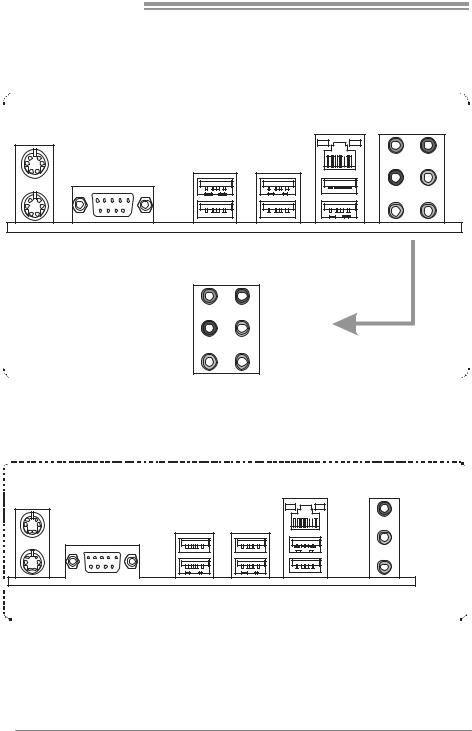
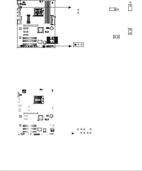
1.4REAR PANEL CONNECTORS (FOR VER 1.X & VER 5.X)
PS/2 |
LAN |
Mouse |
PS/2 |
COM1 |
USBX2 USBX2 USBX2 |
Keyboard |
|
|
|
Center |
Line In |
|
Rear |
Line Out |
|
Side |
Mic In |
1.5REAR PANEL CONNECTORS (FOR VER 6.X)
PS/2 |
|
Mouse |
LAN |
Li ne In/
Surround
Line Out
Mic In 1/
Bass/ Center
|
PS/2 |
COM1 |
USBX2 USBX2 USBX2 |
|
|||
|
|||
|
Keyboar d |
|
|
4

TForce 570 U
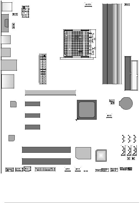
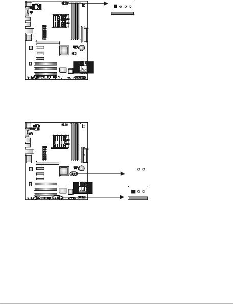
1.6MOTHERBOARD LAYOUT (FOR VER 1.X)
JKBM S1
JKBM SV1
JATXPWR2
1MJCO
JUSBV2
JUSB3 |
JUSB4
JUSBLAN1
JAUDIO1 |
JATXPWR1
PEX16_1
LAN PEX1_1
PEX1_2
JCFAN1
JDDRII_ 2.2V
DDR2A1 |
DDR2B1 |
DDR2A2 |
DDR2B2 |
IDE1 |
FDD1 |
JCMOS1 |
BAT1 |
|
JCI1(o ptiona l) |
||
|
||
nForce |
|
|
570 Ultra |
|
|
JNFAN1 |
|
PEX1_3
JSATA4 JSATA5 JSATA6
Codec |
|
|
|
|
|
|
PCI1 |
|
|
|
|
|
|
|
|
|
|
|
|
|
|
|
|
|
|
|
|
PCI2
PCI3
JCDIN1 JAUDIOF1 JSPDIF_ OUT |
JPRNT1 |
|
Super I/O |
BIOS |
|
|
|
||
|
5SB |
DIMM |
|
|
D_ |
D_ |
|
|
LE |
LE |
|
JSFAN2 |
JSFAN1 |
JUSBV1 |
JUSB2 |
J USB1 |
JSATA1 JSATA2 JSATA3
RSTSW1 PWRSW1
JPANEL1
Not e: ■ represents the 1st pin.
5
Motherboard Manual
1.7MOTHERBOARD LAYOUT (FOR VER 5.X)
JKBM S1
JKBM SV1
JATXPWR2
1MJCO
JUSBV2
JUSB3 |
JUSB4
JUSBLAN1
JAUDIO1 |
JATXPWR1
PEX16_1
LAN PEX1_1
PEX1_2
JCFAN1
JDDRII_2. 4V
DDR2A1 |
DDR2B1 |
DDR2A2 |
DDR2B2 |
IDE1 |
FDD1 |
JCMOS1 |
BAT1 |
JCI1(o ptiona l) |
|
nForce |
|
570 Ultra |
|
JNFAN1 |
|
PEX1_3
JSATA4 JSATA5 JSATA6
Codec |
|
|
|
|
|
|
|
|
PCI1 |
|
|
|
|
|
|
|
|
|
|
|
|
|
|
|
|
|
|
|
|
|
|
|
|
|
|
PCI2
PCI3
JCDIN1 JAUDIOF1 JSPDIF_ OUT |
JPRNT1 |
Super I/O
|
LE D1 |
LE D2 |
JSFAN2 |
JSFAN1 |
|
Not e: ■ represents the 1st pin.
BIOS |
JSATA1 JSATA2 JSATA3 |
|
RSTSW1 PWRSW1 |
JUSBV1 |
JUSB2 |
J USB1 |
JPANEL1 |
6
TForce 570 U
1.8MOTHERBOARD LAYOUT (FOR VER 6.X)
JKBM S1
JKBM SV1
JATXPWR2
1MJCO
JUSBV2
JUSB3 |
JUSB4 |
|
JATXPWR1 |
|||||
|
|
|
|
|
|
|
|
|
|
|
|
|
|
|
|
|
|
|
|
|
|
|
|
JUSBLAN1 |
|
|
|
|
|
|
|
|
|
|
|
|
|
||
|
|
|
|
|
|
||
|
|
|
|
|
|
|
|
|
|
|
|
|
|
|
|
|
|
|
|
|
|
|
|
|
|
|
|
|
|
|
|
JAUDIO2 |
PEX16_1
LAN PEX1_1
PEX1_2
JCFAN1
JDDRII_2. 4V
DDR2A1 |
DDR2B1 |
DDR2A2 |
DDR2B2 |
IDE1 |
FDD1 |
JCMOS1 |
BAT1 |
JCI1(o ptiona l) |
|
nForce |
|
570 Ultra |
|
JNFAN1 |
|
PEX1_3
JSATA4 JSATA5 JSATA6
Codec |
|
|
|
|
|
|
|
|
PCI1 |
|
|
|
|
|
|
|
|
|
|
|
|
|
|
|
|
|
|
|
|
|
|
|
|
|
|
PCI2
PCI3
JCDIN1 JAUDIOF1 JSPDIF_ OUT |
JPRNT1 |
Super I/O
|
LE D1 |
LE D2 |
JSFAN2 |
JSFAN1 |
|
Not e: ■ represents the 1st pin.
BIOS |
JSATA1 JSATA2 JSATA3 |
|
RSTSW1 PWRSW1 |
JUSBV1 |
JUSB2 |
J USB1 |
JPANEL1 |
7
Motherboard Manual
CHAPTER 2: HARDWARE INSTALLATION
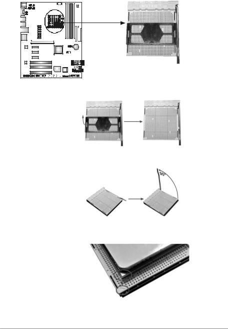
2.1INSTALLING CENTRAL PROCESSING UNIT (CPU)
Step 1: Remove the socket protection cap.
Step 2: Pull the lever toward direction A from the socket and then raise the lever up to a 90-degree angle.
Step 3: Look for the white triangle on socket, and the gold triangle on
CPU should point towards this white triangle. The CPU will fit only in the correct orientation.
8
TForce 570 U
Step 4: Hold the CPU down firmly, and then close the lever toward direct B to complete the installation.
Step 5: Put the CPU Fan on the CPU and buckle it. Connect the CPU FAN power cable to the JCFAN1. This completes the installation.
9
Motherboard Manual
2.2FAN HEADERS
These fan headers support cooling-fans built in the computer. The fan
cable and connector may be different according to the fan manufacturer. Connect the fan cable to the connector while matching the black wire to
pin#1.
JCFAN1: CPU Fan Header
|
JCFAN1 |
1 |
4 |
Pin
1
2
3
4
Assignment
Ground +12V
FAN RPM rate sense
Smart Fan Control (By Fan)
JSFAN1 / JSFAN2: System Fan Header JNFAN1: North Bridge Fan Header
Note: |
|
|
|
Pin |
Assignment |
1 |
3 |
1 |
Ground |
|
2 |
+12V |
|||
|
|
|
JNFAN1 3 |
FAN RPM |
|
|
|
||
|
|
|
|
rate sense |
|
|
|
|
|
|
|
JSFAN1 |
1 |
3 |
JSFAN2 |
|
The JCFAN1 JSFAN1/JSFAN2 and JNFAN1 support 4-pin and 3- pin head connector.
When connecting with wires onto connectors, please note that the red wire is the positive and should be connected to pin#2, and the black wire is Gr ound and should be connected to GND.
10
TForce 570 U
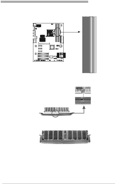
2.3INSTALLING SYSTEM MEMORY
A. Memory Modules
DDR2A1 DDR2B1 |
DDR2A2 DDR2B2 |
1.Unlock a DIMM slot by pressing the retaining clips outward. Align a
DIMM on the slot such that the notch on the DIMM matches the break on the Slot.
2.Insert the DIMM vertically and firmly into the slot until the retaining chip snap back in place and the DIMM is properly seated.
11

Motherboard Manual
B. Memory Capacity
|
|
|
|
|
|
DIMM Socket |
DDR Module |
Total Memory |
|
|
Location |
Size |
|
|
|
|
|
||
|
DDR2A1 |
256MB/512MB/1024MB |
|
|
|
|
|
|
|
|
DDR2B1 |
256MB/512MB/1024MB |
Max is 4GB. |
|
|
DDR2A2 |
256MB/512MB/1024MB |
|
|
|
|
|
||
|
DDR2B2 |
256MB/512MB/1024MB |
|
|
|
|
|
|
|
C. Dual Channel Memory installation
To trigger the Dual Channelf unction of the motherboard, the memory module must meet the following requirements:
Install memory module of the same density in pairs, shown in thef ollowing table.
Dual Channel Status |
DDR2A1 |
DDR2B1 |
DDR2A2 |
DDR2B2 |
Enabled |
O |
O |
X |
X |
|
|
|
|
|
Enabled |
X |
X |
O |
O |
Enabled |
O |
O |
O |
O |
(O means memory installed, X means memory not installed.)
The DRAM bus width of the memory module must be the same (x8 or x16)
12

TForce 570 U
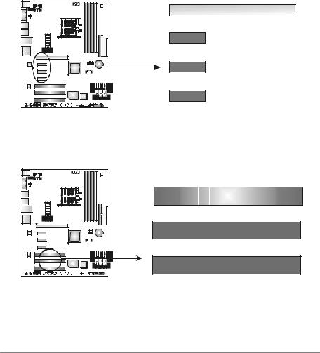
2.4CONNECTORS AND SLOTS
FDD1: Floppy Disk Connector
The motherboard prov ides a standard floppy disk connector that supports 360K, 720K, 1.2M, 1.44M and 2.88M floppy disk ty pes. This connector supports the prov idedf loppy drive ribbon cables.
3 4  33
33
2  1
1
IDE1: Hard Disk Connector
The motherboard has a 32-bit Enhanced IDE Controller that prov ides PIO Mode 0~4, Bus Master, and Ultra DMA 33/66/100/133f unctionality.
The IDE connector can connect a master and a slave drive, soy ou can connect up to two hard disk driv es.
40  39
39
2  1
1
13
Motherboard Manual
PEX16_1: PCI-Express x16 Slot
-PCI-Express 1.0a compliant.
-Maximum theoretical realized bandwidth of 4GB/s simultaneously per direction, f or an aggregate of 8GB/s totally.
PEX1_1/PEX1_2/ PEX1_3: PCI-Express x1 slots
-PCI-Express 1.0a compliant.
- Data transf er bandwidth up to 250MB/s per direction; 500MB/s in total. - PCI-Express supports a raw bit-rate of 2.5Gb/s on the data pins.
-2X bandwidth ov er the traditional PCI architecture.
PEX 16_1
PEX1_1
PEX1_2
PEX1_3
PCI1~PCI3: Peripheral Component Interconnect Slots
This motherboard is equipped with 3 standard PCI slots. PCI stands f or
Peripheral Component Interconnect, and it is a bus standard for expansion cards. This PCI slot is designated as 32 bits.


 PCI1
PCI1
PCI2
PCI3
14
TForce 570 U
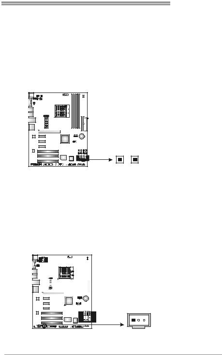
CHAPTER 3: HEADERS & JUMPERS SETUP
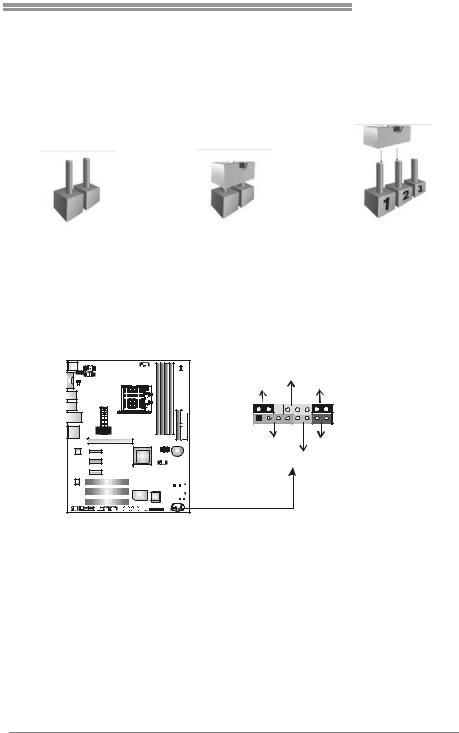
3.1HOW TO SETUP JUMPERS
The illustration shows how to set up jumpers. When the jumper cap is
placed on pins, the jumper is “close”, if not, that means the jumper is “open”.
Pin opened |
Pin closed |
Pin1-2 closed |
3.2DETAIL SETTINGS
JPANEL1: Front Panel Header
This 16-pin connector includes Power-on, Reset, HDD LED, Power LED, Sleep button and speaker connection. It allows user to connect the PC case’s f ront
panel switch functions.
|
PWR_LED |
||
|
SLP |
|
On/Off |
|
|
|
|
9 |
+ + |
- |
16 |
|
|||
|
|
||
1 |
+ |
- |
8 |
|
|
|
|
|
SPK |
|
RST |
|
|
|
|
|
HLED |
||
|
|
|
|
|
|
|
|
|
|
|
|
|
|
|
|
|
|
|
|
|
|
|
|
|
|
|
|
|
|
|
|
|
|
|
|
|
|
|
|
|
|
|
|
|
|
|
|
|
|
|
|
|
|
|
|
|
|
|
|
|
|
|
|
|
|
|
|
|
|
|
|
|
|
|
|
|
|
|
|
|
|
|
|
|
|
|
|
|
|
|
|
|
|
|
|
|
|
|
|
|
|
|
|
|
|
|
|
|
|
|
|
|
|
|
Pin |
|
|
|
|
|
|
|
Assignment |
|
|
Function |
Pin |
Assignment |
Function |
||||||||
1 |
|
|
|
|
|
|
+5V |
|
|
|
9 |
Sleep control |
Sleep button |
|||||||||
2 |
|
|
|
|
|
|
N/A |
|
|
Speaker |
10 |
Ground |
||||||||||
|
|
|
|
|
|
|
|
|
||||||||||||||
3 |
|
|
|
|
|
|
N/A |
|
|
Connector |
11 |
N/A |
N/A |
|||||||||
4 |
|
|
|
|
|
|
Speaker |
|
|
|
12 |
Power LED (+) |
Power LED |
|||||||||
5 |
|
|
|
|
|
|
HDD LED (+) |
|
|
Hard drive |
13 |
Power LED (+) |
||||||||||
6 |
|
|
|
|
|
|
HDD LED (-) |
|
|
LED |
14 |
Power LED (-) |
|
|||||||||
7 |
|
|
|
|
|
|
Ground |
|
|
Reset button |
15 |
Power button |
Power-on button |
|||||||||
8 |
|
|
|
|
|
|
Reset control |
|
|
16 |
Ground |
|||||||||||
|
|
|
|
|
|
|
|
|
|
|||||||||||||
15

Motherboard Manual
JATXPWR1: ATX Power Source Connector
This connector allows user to connect 24-pin power connector on the ATX power supply.
Pin |
Assignment |
1 3


 1
1
2 4 |
|
|
|
12 |
|
|
Pin Assignment
13 |
+3.3V |
1 |
+3.3V |
14 |
-12V |
2 |
+3.3V |
15 |
Ground |
3 |
Ground |
16 |
PS_ON |
4 |
+5V |
17 |
Ground |
5 |
Ground |
18 |
Ground |
6 |
+5V |
19 |
Ground |
7 |
Ground |
20 |
NC |
8 |
PW_OK |
21 |
+5V |
9 |
Standby Voltage+5V |
22 |
+5V |
10 |
+12V |
23 |
+5V |
11 |
+12V |
24 |
Ground |
12 |
+3.3V |
JATXPWR2: ATX Power Source Connector
By connecting this connector, it will provide +12V to CPU power circuit.
1 |
8 |
Assignment |
|
Pin |
|
|
|
|
|
|
|
|
|
|
|
|
|
|
|
|
|
|
|
|
|
|
|
|
|
|
|
|
|
|
|
1 |
+12V |
|
|
|
|
|
|
|
|
|
|
|
|
|
|
|
|
|
|
|
|
|
|
|
|
|
|
|
|
|
|
|
2 |
+12V |
|
|
|
|
|
|
|
|
|
|
|
|
|
|
|
|
|
|
|
|
|
|
|
|
|
|
|
|
|
|
|
||
|
|
|
|
|
|
|
|
|
|
|
|
|
|
|
|
|
|
|
|
|
4 |
|
|
|
|
|
|
|
5 |
3 |
+12V |
|
|
|
|
|
|
|
|
|
|
|
|
|
|
|
|
|
|
|
|
|
|
|
|
|
|
|
|
|
4 |
+12V |
|||
|
|
|
|
|
|
|
|
|
|
|
|
|
|
|
|
|
|
|
|
|
|
|
|
|
|
|
|
|
|
|
||
|
|
|
|
|
|
|
|
|
|
|
|
|
|
|
|
|
|
|
|
|
|
|
|
|
|
|
|
|
|
|
5 |
Ground |
|
|
|
|
|
|
|
|
|
|
|
|
|
|
|
|
|
|
|
|
|
|
|
|
|
|
|
|
|
|
|
||
|
|
|
|
|
|
|
|
|
|
|
|
|
|
|
|
|
|
|
|
|
|
|
|
|
|
|
|
|
|
|
6 |
Ground |
|
|
|
|
|
|
|
|
|
|
|
|
|
|
|
|
|
|
|
|
|
|
|
|
|
|
|
|
|
|
|
||
|
|
|
|
|
|
|
|
|
|
|
|
|
|
|
|
|
|
|
|
|
|
|
|
|
|
|
|
|
|
|
7 |
Ground |
|
|
|
|
|
|
|
|
|
|
|
|
|
|
|
|
|
|
|
|
|
|
|
|
|
|
|
|
|
|
|
||
|
|
|
|
|
|
|
|
|
|
|
|
|
|
|
|
|
|
|
|
|
|
|
|
|
|
|
|
|
|
|
8 |
Ground |
|
|
|
|
|
|
|
|
|
|
|
|
|
|
|
|
|
|
|
|
|
|
|
|
|
|
|
|
|
|
|
||
|
|
|
|
|
|
|
|
|
|
|
|
|
|
|
|
|
|
|
|
|
|
|
|
|
|
|
|
|
|
|
|
|
|
|
|
|
|
|
|
|
|
|
|
|
|
|
|
|
|
|
|
|
|
|
|
|
|
|
|
|
|
|
|
|
|
|
|
|
|
|
|
|
|
|
|
|
|
|
|
|
|
|
|
|
|
|
|
|
|
|
|
|
|
|
|
|
|
|
|
|
|
|
|
|
|
|
|
|
|
|
|
|
|
|
|
|
|
|
|
|
|
|
|
|
|
|
|
|
|
|
|
16

TForce 570 U
JKBMSV1: Power Source Selection Headers for Keyboard/Mouse
Pin 1-2 Close:
JKBMSV1: +5V for PS/2 key board and mouse
Pin 2-3 Close:
JKBMSV1: PS/2 keyboard and mouse are powered with +5V standby v oltage.
|
|
|
|
|
|
|
|
|
|
|
|
|
|
|
|
|
|
|
|
|
|
|
|
|
|
|
|
|
|
|
|
1 |
3 |
|
1 |
3 |
|
||||||||||
|
|
|
|
|
|
|
|
|
|||||||||||||||
|
|
|
|
|
|
|
|
|
|
|
|
|
|
|
|
|
|
|
|
|
|
|
|
|
|
|
|
|
|
|
|
|
|
|
|
|
|
|
|
|
|
|
|
|
|
|
|
Pin 1-2 close
1 3
Pin 2-3 close
JUSB1/JUSB2: Headers for USB 2.0 Ports at Front Panel
This header allows user to connect additional USB cable on the PC f ront panel, and also can be connected with internal USB devices, like USB card reader.
|
|
|
|
|
|
|
|
|
|
|
|
|
|
|
|
|
|
|
|
|
|
|
|
|
Pin |
Assignment |
|
|
|
|
|
|
|
|
|
|
|
|
|
|
|
|
|
|
|
|
|
|
|
|
|
||
|
|
|
|
|
|
|
|
|
|
|
|
|
|
|
|
|
|
|
|
|
|
|
|
|
||
|
|
|
|
|
|
|
|
|
|
|
|
|
|
|
|
|
|
|
|
|
|
|
|
|
1 |
+5V (fused) |
|
|
|
|
|
|
|
|
|
|
|
|
|
|
|
|
|
|
|
|
|
|
|
|
|
2 |
+5V (fused) |
|
|
|
|
|
|
|
|
|
|
|
|
|
|
|
|
|
|
|
|
|
|
|
|
|
3 |
USB- |
|
|
|
|
|
|
|
|
|
|
|
|
|
|
|
|
|
|
|
|
|
|
|
|
|
4 |
USB- |
|
|
|
|
|
|
|
|
|
|
|
|
|
|
|
|
|
|
|
|
|
|
|
|
|
||
|
|
|
|
|
|
|
|
|
|
|
|
|
|
|
|
|
|
|
|
|
|
|
|
|
5 |
USB+ |
|
|
|
|
|
|
|
|
|
|
|
|
|
|
|
|
|
|
|
|
|
|
|
|
|
6 |
USB+ |
|
|
|
|
|
|
|
|
|
|
|
|
|
|
|
|
|
|
|
|
|
|
|
|
|
||
|
|
|
|
|
|
|
|
|
|
|
|
|
|
|
|
|
|
|
|
|
|
|
|
|
||
|
|
|
|
|
|
|
|
|
|
|
|
|
|
|
|
|
|
|
|
JUSB2 JUSB1 |
7 |
Ground |
||||
|
|
|
|
|
|
|
|
|
|
|
|
|
|
|
|
|
|
|
|
|||||||
|
|
|
|
|
|
|
|
|
|
|
|
|
|
|
|
|
|
|
|
8 |
Ground |
|||||
|
|
|
|
|
|
|
|
|
|
|
|
|
|
|
|
|
|
|
|
2 |
|
|
|
1 0 |
9 |
Key |
|
|
|
|
|
|
|
|
|
|
|
|
|
|
|
|
|
|
|
10 |
NC |
||||||
|
|
|
|
|
|
|
|
|
|
|
|
|
|
|
|
|
|
|
|
1 |
|
|
|
9 |
|
|
|
|
|
|
|
|
|
|
|
|
|
|
|
|
|
|
|
|
|
|
|
|
|
|
|
|
|
17
Motherboard Manual
JUSBV1/JUSBV2: Power Source Headers for USB Ports
Pin 1-2 Close:
JUSBV1: +5V for USB ports at JUSBLAN1.
JUSBV2: +5V for USB ports at f ront panel (JUSB1/JUSB2).
Pin 2-3 Close:
JUSBV1: USB ports at JUSBLAN1 are powered by +5V standby voltage.
JUSBV2: USB ports at front panel (JUSB1/JUSB2) are powered by +5V standby v oltage.
Note: |
JUSBV2 |
|
|
|
3 |
|
|
|
|||||
|
|
|
|
|
|
|||||||
1 |
|
|
|
|
1 |
3 |
1 |
|
|
|
||
|
|
|
|
|
|
|
|
|
|
|
||
3 |
|
|
|
|
|
|
|
|
|
|
|
|
|
|
|
|
|
|
|
|
|
|
|
||
|
|
|
|
Pin 1-2 close |
|
|
|
|||||
|
|
|
|
|
|
|
|
|||||
JUSBV1 |
1 |
3 |
|
|
|
|||||||
|
|
|
||||||||||
3 |
|
|
|
|
||||||||
1 |
3 |
|
|
|
|
1 |
|
|
|
|||
|
|
|
|
|
|
|
||||||
|
|
|
|
|
|
|
|
|||||
Pin 2-3 close
In order to support this function “Power-On system vi a USB device,” “JUSBV1/ JUSBV2” jumper cap should be placed on Pin 2-3 indi viduall y.
JAUDIOF1: Front Panel Audio Header
This header allows user to connect the front audio output cable with the PC f ront panel. It will disable the output on back panel audio connectors.
|
|
|
|
|
|
|
|
|
|
|
|
|
|
|
|
|
|
|
|
|
|
|
Pin |
Assignment |
|
|
|
|
|
|
|
|
|
|
|
|
|
|
|
|
|
|
|
|
|
|
|
1 |
Mic in |
|
|
|
|
|
|
|
|
|
|
|
|
|
|
|
|
|
|
|
|
|
|
|
||
|
|
|
|
|
|
|
|
|
|
|
|
|
|
|
|
|
|
|
|
|
|
|
||
|
|
|
|
|
|
|
|
|
|
|
|
|
|
|
|
|
|
|
|
|
|
|
2 |
Ground |
|
|
|
|
|
|
|
|
|
|
|
|
|
|
|
|
|
|
|
|
|
|
|
3 |
Mic power |
|
|
|
|
|
|
|
|
|
|
|
|
|
|
|
|
|
|
|
|
|
|
|
4 |
Audio power |
|
|
|
|
|
|
|
|
|
|
|
|
|
|
|
|
|
|
|
|
|
|
|
5 |
Right line out |
|
|
|
|
|
|
|
|
|
|
|
|
|
|
|
|
|
|
|
|
|
|
|
||
|
|
|
|
|
|
|
|
|
|
|
|
|
|
|
|
|
|
|
|
|
|
|
||
|
|
|
|
|
|
|
|
|
|
|
|
|
|
|
|
|
|
|
|
|
|
|
6 |
Right line out |
|
|
|
|
|
|
|
|
|
|
|
|
|
|
|
|
|
|
|
|
|
|
|
||
|
|
|
|
|
|
|
|
|
|
|
|
|
|
|
|
|
|
|
|
|
|
|
7 |
Reserved |
|
|
|
|
|
|
|
|
|
|
|
|
|
|
|
|
|
|
|
|
|
|
|
8 |
Key |
|
|
|
|
|
|
|
|
|
|
|
|
|
|
|
|
|
|
2 |
10 |
9 |
Left line ou |
|||
|
|
|
|
|
|
|
|
|
|
|
|
|
|
|
|
|
|
|||||||
|
|
|
|
|
|
|
|
|
|
|
|
|
|
|
|
|
|
|
|
|
|
|
10 |
LFT Line Out |
|
|
|
|
|
|
|
|
|
|
|
|
|
|
|
|
|
|
|
|
|
|
|
|
|
|
|
|
|
|
|
|
|
|
|
|
|
|
|
|
|
|
|
|
|
|
|
|
|
|
|
|
|
|
|
|
|
|
|
|
|
|
|
|
|
|
|
|
|
1 |
9 |
|
|
|
|
|
|
|
|
|
|
|
|
|
|
|
|
|
|
|
|
|
|
|
|
|||||
18
TForce 570 U
JCDIN1: CD-ROM Audio-in Connector
This connector allows user to connect the audio sourcef rom thev ariaty dev ices, like CD-ROM, DVD-ROM, PCI sound card, PCI TV turner card etc.
|
|
|
|
|
|
|
|
|
|
|
|
|
|
|
|
|
|
|
|
|
|
|
Pin |
Assignment |
|
|
|
|
|
|
|
|
|
|
|
|
|
|
|
|
|
|
|
|
|
|
|
||
|
|
|
|
|
|
|
|
|
|
|
|
|
|
|
|
|
|
|
|
|
|
|
||
|
|
|
|
|
|
|
|
|
|
|
|
|
|
|
|
|
|
|
|
|
|
|
||
|
|
|
|
|
|
|
|
|
|
|
|
|
|
|
|
|
|
|
|
|
|
|
||
|
|
|
|
|
|
|
|
|
|
|
|
|
|
|
|
|
|
|
|
|
|
|
||
|
|
|
|
|
|
|
|
|
|
|
|
|
|
|
|
|
|
|
|
|
|
|
1 |
Left Channel Input |
|
|
|
|
|
|
|
|
|
|
|
|
|
|
|
|
|
|
|
|
|
|
|
||
|
|
|
|
|
|
|
|
|
|
|
|
|
|
|
|
|
|
|
|
|
|
|
2 |
Ground |
|
|
|
|
|
|
|
|
|
|
|
|
|
|
|
|
|
|
|
3 |
Ground |
||||
|
|
|
|
|
|
|
|
|
|
|
|
|
|
|
|
4 |
Right Channel Input |
|||||||
|
|
|
|
|
|
|
|
|
|
|
|
|
|
|
|
|
|
|
||||||
|
|
|
|
|
|
|
|
|
|
|
|
|
|
|
|
|
|
|
|
|
|
|
|
|
1 4
JCMOS1: ClearCMOS Header
By placing the jumper on pin2-3, it allows user to restore the BIOS saf e setting
and the CMOS data, please carefully f ollow the procedures to avoid damaging the motherboard.
1 3
Pin 1-2 Close:
Normal Operation (default).
1 3 


 1 3
1 3
Pin 2-3 Close:
Clear CMOS data.
Clear CMOS Procedures:
1.Remov e AC power line.
2.Set the jumper to “Pin 2-3 close”.
3.Wait f orf ive seconds.
4.Set the jumper to “Pin 1-2 close”.
5.Power on the AC.
6.Reset y our desired password or clear the CMOS data.
19
Motherboard Manual
JCI1: Chassis Open Header (Optional)
This connector allows system to monitor PC case open status. If the signal has been triggered, it will record to the CMOS and show the message on next
boot-up.
|
|
|
|
|
|
|
|
|
|
|
Pin |
Assignment |
|
|
|
|
|
|
|
|
|
|
|
||
|
|
|
|
|
|
|
|
|
|
|
||
|
|
|
|
|
|
|
|
|
|
|
||
|
|
|
|
|
|
|
|
|
|
|
||
|
|
|
|
|
|
|
|
|
|
|
||
|
|
|
|
|
|
|
|
|
|
|
||
|
|
|
|
|
|
|
|
|
|
|
||
|
|
|
|
|
|
|
1 |
|
1 |
Case open |
||
|
|
|
|
|
|
|
|
|||||
|
|
|
|
|
|
|
|
|
|
|
|
signal |
|
|
|
|
|
|
|
|
|
|
|
|
|
|
|
|
|
|
|
|
|
|
|
|
2 |
Ground |
|
|
|
|
|
|
|
|
|
|
|
|
|
|
|
|
|
|
|
|
|
|
|
|
|
|
|
|
|
|
|
|
|
|
|
|
|
|
|
|
|
|
|
|
|
|
|
|
|
|
|
|
|
|
|
|
|
|
|
|
|
|
|
|
|
|
|
|
|
|
|
|
|
|
|
|
|
|
|
|
|
|
|
|
|
|
|
|
|
|
|
|
|
|
|
|
|
|
|
|
|
|
|
|
JPRNT1: Printer Port Connector
This header allows you to connector printer on the PC.
|
|
|
|
|
|
|
|
|
|
|
|
|
|
|
|
|
|
2 5 |
|
1 |
|
||||
|
|
|
|
|
|
|
|
|
|
|
|
|
|
|
|
|
|
|
|
||||||
|
|
|
|
|
|
|
|
|
|
|
|
|
|
|
|
|
|
|
|
||||||
|
|
|
|
|
|
|
|
|
|
|
|
|
|
|
|
|
|
|
|
||||||
|
|
|
|
|
|
|
|
|
|
|
|
|
|
|
|
|
|
|
|
||||||
|
|
|
|
|
|
|
|
|
|
|
|
|
|
|
|
|
|
|
|
||||||
|
|
|
|
|
|
|
|
|
|
|
|
|
|
|
|
|
|
|
|
||||||
|
|
|
|
|
|
|
|
|
|
|
|
|
|
|
|
|
|
|
|
||||||
|
|
|
|
|
|
|
|
|
|
|
|
|
|
|
|
|
|
|
|
||||||
|
|
|
|
|
|
|
|
|
|
|
|
|
|
|
|
|
|
|
|
||||||
|
|
|
|
|
|
|
|
|
|
|
|
|
|
|
|
|
|
|
|
||||||
|
|
|
|
|
|
|
|
|
|
|
|
|
|
|
|
|
|
|
|
||||||
|
|
|
|
|
|
|
|
|
|
|
|
|
|
|
|
|
|
|
|||||||
|
|
|
|
|
|
|
|
|
|
|
|
|
|
|
|
|
|
|
|
|
|
|
|
|
|
|
|
|
|
|
|
|
|
|
|
|
|
|
|
|
|
|
|
|
|
|
|
|
|
|
|
|
|
|
|
|
|
|
|
|
|
|
|
|
|
|
|
|
|
|
|
|
|
|
|
|
|
|
|
|
|
|
|
|
|
|
|
|
|
|
|
|
|
|
|
|
|
|
|
|
|
|
|
|
|
|
|
|
|
|
|
|
|
|
|
|
|
|
|
|
|
|
|
|
|
2 |
|
|
|
|
|
|
|
|
|
|
|
|
|
|
|
|
|
|
|
|
|
|
|
|
|
||||
|
|
|
|
|
|
|
|
|
|
|
|
|
|
|
|
||||||||||
|
Pin |
|
|
|
|
|
|
|
|
|
|
|
Assignment |
Pin |
Assignment |
||||||||||
|
1 |
|
|
|
|
|
|
|
-Strobe |
14 |
Ground |
||||||||||||||
|
2 |
|
|
|
|
|
|
|
-ALF |
15 |
Data 6 |
||||||||||||||
|
3 |
|
|
|
|
|
|
|
Data 0 |
16 |
Ground |
||||||||||||||
|
4 |
|
|
|
|
|
|
|
-Error |
17 |
Data 7 |
||||||||||||||
|
5 |
|
|
|
|
|
|
|
Data 1 |
18 |
Ground |
||||||||||||||
|
6 |
|
|
|
|
|
|
|
-Init |
19 |
-ACK |
||||||||||||||
|
7 |
|
|
|
|
|
|
|
Data 2 |
20 |
Ground |
||||||||||||||
|
8 |
|
|
|
|
|
|
|
-Scltin |
21 |
Busy |
||||||||||||||
|
9 |
|
|
|
|
|
|
|
Data 3 |
22 |
Ground |
||||||||||||||
|
10 |
|
|
|
|
|
|
Ground |
23 |
PE |
|||||||||||||||
|
11 |
|
|
|
|
|
|
Data 4 |
24 |
Ground |
|||||||||||||||
|
12 |
|
|
|
|
|
|
Ground |
25 |
SCLT |
|||||||||||||||
|
13 |
|
|
|
|
|
|
Data 5 |
26 |
Key |
|||||||||||||||
20

TForce 570 U
JSATA1~JSATA6: Serial ATA Connectors
The motherboard has a PCI to SATA Controller with 6 channels SATA interf ace, it satisfies the SATA 2.0 spec and with transfer rate of 3.0Gb/s.
|
|
|
|
|
|
|
|
|
|
|
|
|
|
JSATA4 JSATA5 JSATA6 |
Pin |
Assignment |
|||||
|
|
|
|
|
|
|
|
|
|
|
|
|
|
||||||||
|
|
|
|
|
|
|
|
|
|
|
|
|
|
||||||||
|
|
|
|
|
|
|
|
|
|
|
|
|
|
||||||||
|
|
|
|
|
|
|
|
|
|
|
|
|
|
||||||||
|
|
|
|
|
|
|
|
|
|
|
|
|
|
||||||||
|
|
|
|
|
|
|
|
|
|
|
|
|
|
1 |
Ground |
||||||
|
|
|
|
|
|
|
|
|
|
|
|
|
|||||||||
|
|
|
|
|
|
|
|
|
|
|
|
|
7 |
|
|
|
|
2 |
TX+ |
||
|
|
|
|
|
|
|
|
|
|
|
|
|
|
|
|
|
|||||
|
|
|
|
|
|
|
|
|
|
|
|
|
|
|
|
|
3 |
TX- |
|||
|
|
|
|
|
|
|
|
|
|
|
|
|
|
|
|
|
|
|
|
4 |
Ground |
|
|
|
|
|
|
|
|
|
|
|
|
|
|
|
|
|
|
|
|
||
|
|
|
|
|
|
|
|
|
|
4 |
|
|
|
|
|||||||
|
|
|
|
|
|
|
|
|
|
|
|
|
|
5 |
RX- |
||||||
|
|
|
|
|
|
|
|
|
|
|
|
|
|
|
|
|
|
|
|
||
|
|
|
|
|
|
|
|
|
|
|
|
|
1 |
|
|
|
|
6 |
RX+ |
||
|
|
|
|
|
|
|
|
|
|
|
|
|
|
|
|
|
|
|
|
7 |
Ground |
|
|
|
|
|
|
|
|
|
|
|
|
|
|
|
|
|
|
|
|
|
|
JSATA1 JSATA2 JSATA3
Header for Memory over-voltage: JDDRII_2.2V (for Ver 1.x)
When processing Memory ov er-voltage, please place the jumper to pin2-3 Closed. The Def ault setting is Pin 1-2 Closed.
3 |
3 |
1 |
1 |
|
Pin 1-2 Close: |
|
Normal status (default). |
|
3 |
|
1 |
|
Pin 2-3 Close: |
|
Memory voltage 2.2V. |
Note: |
|
1.When “JDDRII_2.2V” jumper cap is placed on Pin 1-2, memory v oltage can be manually adjusted in CMOS setup screen.
2.When “JDDRII_2.2V” jumper cap is placed on Pin 2-3, memory v oltage will be f ixed at 2.2V automatically, and can’t be adjusted under COMS setup.
Bef oresetting memory over-v oltage, please ensure that your DDR2 supports up to 2.2V. (Consult your DDR2 supplier)
21

Motherboard Manual
Header for Memory over-voltage: JDDRII_2.4V (for Ver 5.x/6.x)
When processing Memory ov er-voltage, please place the jumper to pin2-3 Closed. The Def ault setting is Pin 1-2 Closed.
1 |
3 |
3 |
|
1 |
|
|
Pin 1-2 Close: |
|
|
Normal status (default). |
|
|
1 |
3 |
|
Pin 2-3 Close: |
|
|
Memory voltage 2.4V. |
|
Note: |
|
|
3.When “JDDRII_2.4V” jumper cap is placed on Pin 1-2, memory v oltage can be manually adjusted in CMOS setup screen.
4.When “JDDRII_2.4V” jumper cap is placed on Pin 2-3, memory v oltage
will be f ixed at 2.4V automatically, and can’t be adjusted under COMS setup.
Bef oresetting memory over-v oltage, please ensure that your DDR2 supports up to 2.4V. (Consult your DDR2 supplier)
On-Board LED Indicators
There are 2 LED indicators on the motherboard to show system status.
Ver 1.x |
Ver 5.x/6.x |
LED_5SB |
|
LED_DIMM |
LED1 LED2 |
LED_DIMM:
This LED indicates the voltage of memory is activated normally.
LED_5SB:
This LED indicates the system is ready for Power-on.
22
TForce 570 U
LED1 and LED2:
These 2 LED indicate system power on diagnostics. Please ref er to thetable below for different messages:
|
|
|
|
|
|
LED1 |
LED2 |
Message |
|
|
ON |
ON |
Normal |
|
|
ON |
OFF |
VGA Error |
|
|
OFF |
ON |
Memory Error |
|
|
OFF |
OFF |
Abnormal: CPU / Chipset error. |
|
|
|
|
|
|
On-Board Buttons
There are 2 on-board buttons.
RSTSW1 PWRSW1
PWRSW1:
This is an on-board Power Switch button.
RSTSW1:
This is an on-board Reset button.
JSPDIF_OUT1: Digital Audio-outConnector
This connector allows user to connect the PCI bracket SPDIF output header.
|
|
|
|
|
|
|
|
|
|
|
|
|
|
|
|
|
|
Pin |
Assignment |
|
|
|
|
|
|
|
|
|
|
|
|
|
|
|
|
|
|
||
|
|
|
|
|
|
|
|
|
|
|
|
|
|
|
|
|
|
||
|
|
|
|
|
|
|
|
|
|
|
|
|
|
|
|
|
|
||
|
|
|
|
|
|
|
|
|
|
|
|
|
|
|
|
|
|
||
|
|
|
|
|
|
|
|
|
|
|
|
|
|
|
|
|
|
||
|
|
|
|
|
|
|
|
|
|
|
|
|
|
|
|
|
|
||
|
|
|
|
|
|
|
|
|
|
|
|
|
|
|
|
|
|
||
|
|
|
|
|
|
|
|
|
|
|
|
|
|
|
|
|
|
1 |
+5V |
|
|
|
|
|
|
|
|
|
|
|
|
|
|
|
|
|
|
||
|
|
|
|
|
|
|
|
|
|
|
|
|
|
|
|
|
|
2 |
SPDIF_OUT |
|
|
|
|
|
|
|
|
|
|
|
|
|
|
|
|
|
|
||
|
|
|
|
|
|
|
|
|
|
|
|
|
|
|
|
|
3 |
Ground |
|
|
|
|
|
|
|
|
|
|
|
|
|
|
|
|
|
|
|||
|
|
|
|
|
|
|
|
|
|
|
|
|
|
|
|
|
|
|
|
1 3
23
Motherboard Manual
CHAPTER 4: NVIDIA RAID FUNCTIONS
4.1OPERATION SYSTEM
Supports Windows XP Home/Prof essional Edition, and Windows 2000 Professional.
4.2RAID ARRAYS
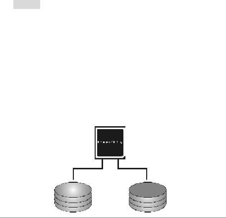
NVRAID supports thef ollowing ty pes of RAID arrays:
RAID 0: RAID 0 defines a disk striping scheme that improves disk read and write times for many applications.
RAID 1: RAID 1 defines techniques for mirroring data.
RAID 0+1: RAID 0+1 combines the techniques used in RAID 0 and RAID 1.
Spanning (JBOD): JBOD provides a method for combining drives ofdifferent sizes in to one large disk.
RAID 5: RAID 5 provides fault tolerance and better utilization of disk capacity.
4.3HOW RAID WORKS
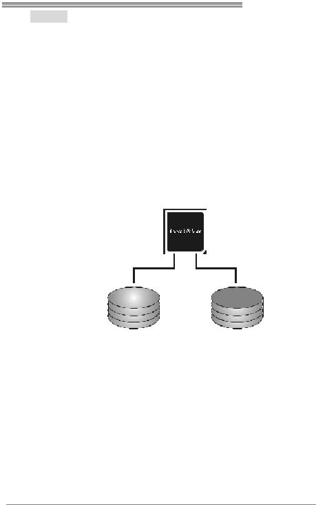
RAID 0:
The controller “stripes” data across multiple drives in a RAID 0 array system. It breaks
up a large file into smaller blocks and performs disk reads and writes across multiple drives in parallel. The size of each block is determined by the stripe size parameter, which you set during the creation ofthe RAID set based on the systemenvironment. This
technique reduces overall disk access time and offers high bandwidth.
Features and Benefits
Drives: Minimum 1, and maximum is up to 6 or 8. Depending on the platf orm.
Uses: Intended for non-critical data requiring high data throughput, or any
env ironment that does not requiref ault tolerance.
Benefits: prov ides increased data throughput, especially f or large files. No
capacity loss penalty f or parity.
Drawbacks: Does not deliver any fault tolerance. If any drive in the array f ails, all data is lost.
Fault Tolerance: No.
Block 1 |
|
|
|
Block 2 |
|
|
|
||
|
|
|
||
|
|
|
||
Block 3 |
|
|
|
Bl ock 4 |
Block 5 |
|
|
|
Bl ock 6 |
24
TForce 570 U
RAID 1:
Every read and write is actually carried out in parallel across 2 disk drives in a RAID 1
array system. The mirrored (backup) copy ofthe data can reside on the same disk or on a second redundant drive in the array. RAID 1 provides a hot-standby copy of data if the active volume or drive is corrupted or becomes unavailable because ofa hardware
failure.
RAID techniques can be applied for high-availability solutions, or as a form of automatic backup that eliminates tedious manual backups to more expensive and less
reliable media.
Features and Benefits
Drives: Minimum 2, and maximum is 2.
Uses: RAID 1 is idealfor small databases or any other applicationthat requires f ault tolerance and minimal capacity.
Benefits: Prov ides 100% data redundancy. Should one driv ef ail, the controller switches to the other drive.
Drawbacks: Requires 2 driv es for the storage space of one driv e. Perf ormance is impaired during driv e rebuilds.
Fault Tolerance: Yes.
Block 1 |
|
|
|
Block 1 |
|
|
|
||
|
|
|
||
Block 2 |
|
|
|
Block 2 |
Block 3 |
|
|
|
Block 3 |
25
Motherboard Manual
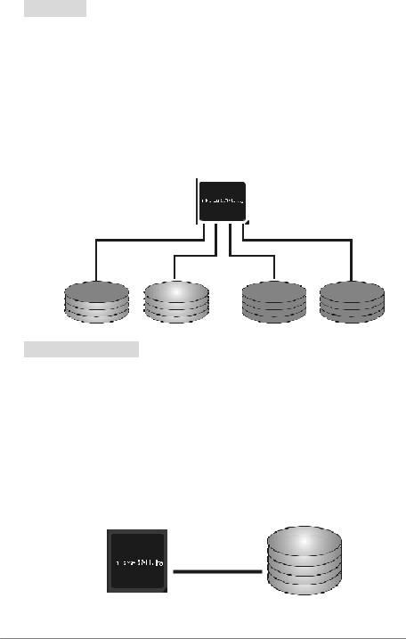
RAID 0+1:
RAID 0 drives can be mirrored using RAID 1 techniques. Resulting in a RAID 0+1 solution for improved performance plus resiliency.
Features and Benefits
-Drives: Minimum 4, and maximum is 6 or 8, depending on the platform.
-Benefits: Optimizes for both fault tolerance and perf ormance, allowing for
automatic redundancy. May be simultaneously used with other RAID lev els in an array, and allows f or spare disks.
-Drawbacks: Requires twice the av ailable disk spacef or data redundancy, the same as RAID level 1.
-Fault Tolerance: Yes.
Block 1 |
|
Block 2 |
|
|
|
Block 1 |
|
Block 2 |
|
|
|
|
|
||||
|
|
|
|
|
||||
|
|
|
|
|
||||
Block 3 |
|
Block 4 |
|
|
|
Block 3 |
|
Block 4 |
Block 5 |
Block 6 |
|
|
|
Block 5 |
|
Block 6 |
|
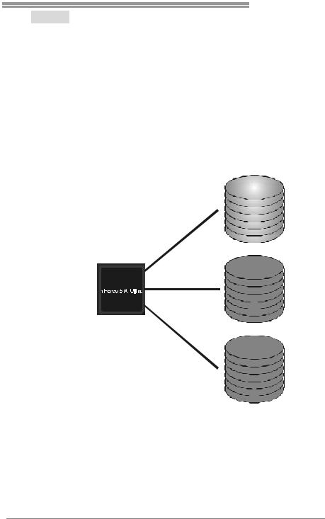
Spanning (JBOD):
JBOD stands for “ Just a Bunch of Disks”. Each drive is accessed as if it were on a standard SCSI host bus adapter. This is useful when a single drive configuration is needed, but it offers no speed improvement or fault tolerance.
Features and Benefits
-Uses: JBOD works best if y ou hav e odd sized driv es andy ou want to combine them to make one big drive.
-Benefits:JBOD prov ides the ability to combine oddsize driv es using all of
the capacity of the driv es.
-Drawbacks: Decreases performance because of the difficulty in using driv es concurrently.
-Fault Tolerance: Yes.
Single Logical
Drive
Disk 1: 40GB
Disk 2: 80GB
Disk 3: 40GB
Disk 4: 120GB
26
TForce 570 U
RAID 5:
RAID 5 stripes both data and parity information across three or more drives. It writes
data and parity blocks across all the drives in the array. Fault tolerance is maintained by ensuring that the parity information for any given block of data is placed on a different drive fromthose used to store the data itself.
Features and Benefits
-Drives: Minimum 3.
-Uses: RAID 5 is recommended for transaction processing and general purpose service.
-Benefits:An ideal combination of good performance, good fault tolerance, and high capacity and storage efficiency.
-Drawbacks: Individual block data transfer rate same as a single disk. Write performance can be CPU intensive.
-Fault Tolerance: Yes.
Di sk 1
DATA 1
DATA 3
PARITY
DATA 7
DATA 9
PARITY
Di sk 2
DATA 2
PARITY
DATA5
DATA8
PARITY
DATA 11
Di sk 3
PARITY
DATA 4
DATA 6
PARITY
DATA 10
DATA 12
For more detailed setup information, please refer to the Driver CD, or go to
http://www.nvidia.com/page/pg_20011106217193.html to download NVIDIA nForce Tutorial Flash.
27

Motherboard Manual
CHAPTER 5: OVERCLOCK QUICK GUIDE
5.1T-POWER INTRODUCTION
Biostar T-Power is a whole new utility that is designed for overclock users. Based on many precise tests, Biostar Engineering Team (BET) has developed this ultimate overclock engine to raise system performance. No matter whether under BIOS or Windows interface, T-Power is able to present the best system state according to users’ overclock setting.
T-Power BIOS Features:
Ov erclocking Nav igator Engine (O.N.E.)
CMOS Reloading Program (C.R.P.)
Memory Integration Test (M.I.T., under Ov erclock Nav igator Engine)
Integrated Flash Program (I.F.P.)
Smart Fan Function (under PC Health Status)
Self Recov ery System (S.R.S)
T-Power Windows Feature:
Hardware Monitor
Ov erclock Engine
Smart Fan Function Lif e Update
28
 Loading...