


P4TSP-D2

P
i
4
T
S
P
-
D
2
P
P
4
T
S
P
4
T
S
P
-
D
2
-
D
2
FCC Infor mation and Copyright
This equipment has been tested and found to com ply with the limits of a
Class B digital device, pursuant to Part 15 of the FCC Rules. T hese limits
are designed to provide reasonable protection against harmful
int erference in a residential ins t allation. This equipment g enerat es, uses
and can radiate radio frequency energy and, if not installed and used i n
ac cordan ce wit h the in stru ction s, ma y cau se harm fu l in terf eren ce t o radi o
communications. There is no guarantee th at interference will not occur in
a partic ular installation.
The vendor makes no repr esentations or warranties with respect to the
contents here of and specially disclaims any implied
merchantabi li ty or fitness fo r a ny purpose. F urther the vendor reserves
the right to revise this publication and to make changes to the contents
here of without obligation to notify any party beforehand.
Duplication of this publication, in part or in whole, is not allowed without
first obtaining the vendor’s approval in writing.
The con tent of this user’s manual is subject to be changed without notice
and we will not be responsible for any mistakes found in this user’s
manual. All the brand and product names are trademarks of their
r es p e c t iv e co m pa ni e s.
warran ties of

C
C
C
n
o
n
o
s
t
n
e
t
s
t
n
e
t
s
t
n
e
t
n
o
LAYOUT OF P4TSP-D2 VERSION 1.X.................................................1
COMPONENT INDEX FOR P4TSP-D2 V.1.X......................................2
LAYOUT OF P4TSP-D2 VERSION 7.X.................................................3
ENGLISH...................................................................................................4
P4TSP-D2 Features....................................................................................4
Packag e contents.......................................................................................5
How to set up a Jumper?............................................................................6
CPU Ins t alla tion......... ........................ ........................................................6
DDR DIMM Modu les: DD RA1/ DDRA2 ...........................................................7
Inst allin g DDR Module ........................................................................ ........7
Jumpers, Headers, Connectors & Slots.........................................................8
DEUT SCH................................................................................................15
Die Spezifikationen von P4TSP-D2............................................................. 15
Verpackungsinhalt...................................................................................17
Einstellung der Jumper.............................................................................17
Inst alla tion der CP U.... ........................ ........................ ........................ ......17
DDR-DIMM-Modules: DDRA1/ DD RA2.........................................................18
Installation von DD R-Modul....................................................................... 19
Jumpers, Headers, Anschlüsse & Slots....................................................... 19
FRANÇAIS .............................................................................................. 27
Caractéristiques de P4TSP-D2...................................................................27
Co nt enu de l'Emballage.......................................................... ..................28
WA RPSPE EDE R
Introdu ction.............................................................................................29
System Requirement................................................................................29
Installation ..............................................................................................30
Usage.....................................................................................................31
TM
................................................................................ 29
TROUBLE SHOOTIN G......................................................................... 39
PROBLEMLÖSUNG.............................................................................. 40
ii
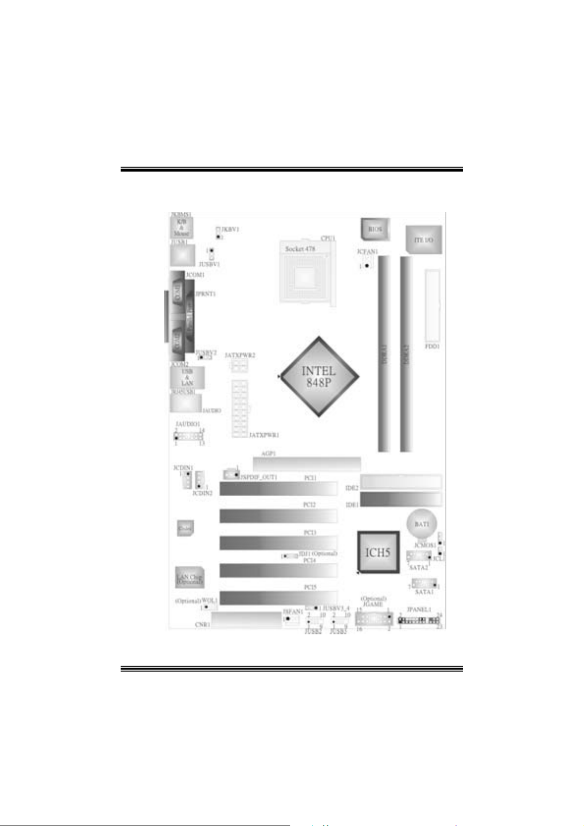
Layout of P4TSP-D2 Version 1.x
NOTE: ●represents the first pin.
1
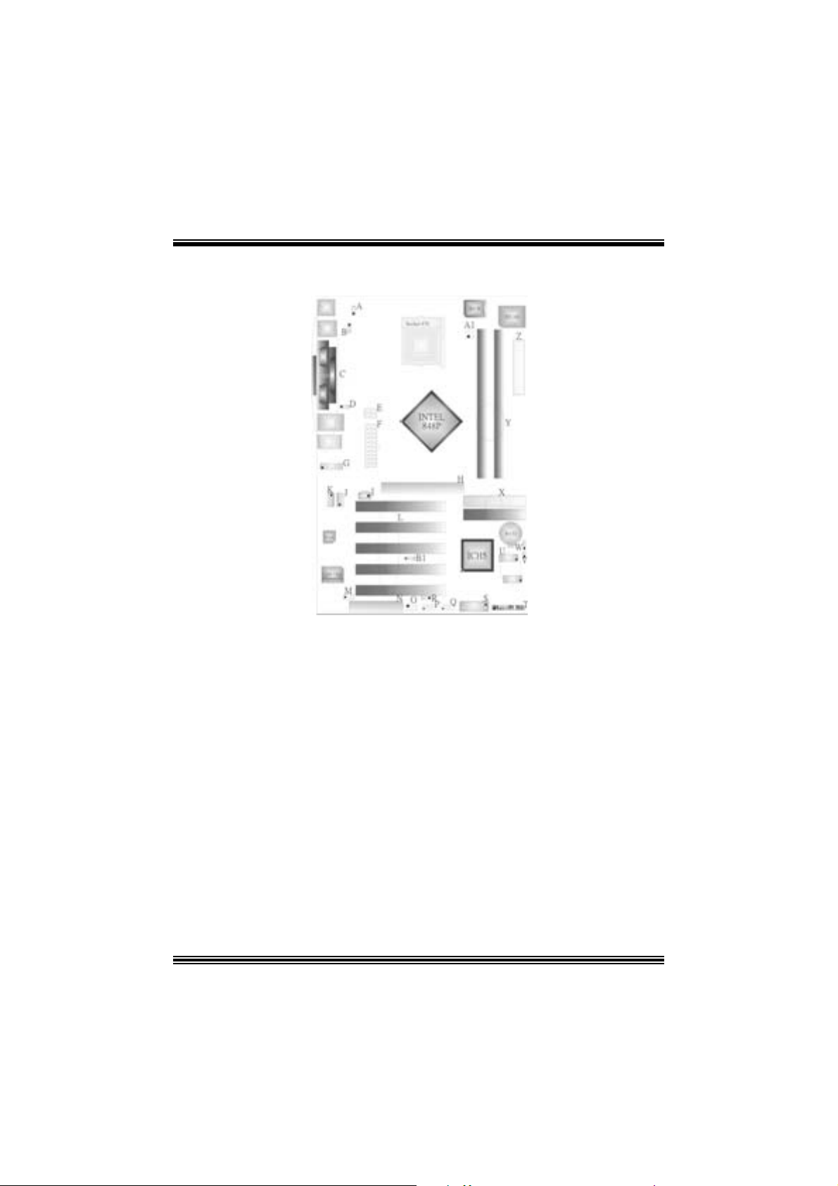
Co mponent Index fo r P4TSP-D2 Versio n 1.x
A. Power Source Selection for Keybo ard and N. Communicatio n Network Riser Slot (CNR1 )
Mouse (JKBV1) O . System FAN H eader (JSFAN1)
B. Power Sour ce Selection for USB P. F ront USB Head er (JUSB2 )
(J USBV1) Q. Front USB Head er (JUSB3)
C. Back Panel Connector R. Power Source Selection for USB
D. Power Source Selection for USB (JUSBV3_4)
(J USB V2) S. Game Port Header (JGAME1): Op tiona l
E. ATX 12V Powe r Connector (JATXPW R2) T. Front Panel Connector (JPANEL1)
F. ATX 12V Po wer Connector (J ATXPW R1) U. Serial ATA Connector (SA TA1-2)
G. Front Audio Head er (JAUDIO1) V. Case Open Connector (JCL1)
H. A cc elera ted Gr aphics Po rt Slot (AGP1) W. Clear C MOS Function (J CMOS1)
I. Digital A udio Connector (JSPDIF_OUT1) X. I DE Connec tors (IDE1-2)
J . CD-ROM Audio-In Header (JCDIN2) Y. DDR DIMM Modul es (DDRA1/ DDRA2)
K. CD-RO M Audio-In Header (JCDI N1) Z. Flopp y Disk Connector (FDD1 )
L. PCI BUS S lots (PCI 1-5) A1. CPU Fan Connector (JCFA N1)
M. W ake On LAN Header (WOL1): Optional B1. Audio DJ Connecto r (JDJ1): O p tional
2
Layout of P4TSP-D2 Versio n 7. x
NOTE: ●represents the first pin.
3

English
P4TSP-D 2 Fe a tu r es
A. Har dware
CPU
Prov ides Sock et 478.
Supports the Intel® Pent ium® 4 processor to 3.2GH z.
Supports the Intel® Pent ium® 4 Northwood CPU. (Willamet t e not support ed)
Supports the Intel® Pent ium® 4 478-pin Prescott C PU.
F ront Side Bus at 400/533/800MHz.
Su pports Hyper-Threading Technology.
Chipset
North Bridge: Intel 848P.
South Bridge: Intel ICH 5.
Main Me m o ry
Supports 64-bit wide DDR data channels with 2 DIMMs.
Av ailable bandwidt h up to 3.2GB/s (DDR 400) for single-channel mode.
Supports 128-Mb, 256-Mb, 512-Mb D DR t ec hnologies .
Supports only x8, x16, DDR devices.
Supports four bank devices.
Maxi mu m me mo ry s i ze is 2GB.
Super I/O
Chip: ITE IT 8712.
Low Pin C ount Int erface.
Prov ides the most commonly used legacy Super I/O f unctionality.
Env iro nm ent C ont rol i niti atives ,
- H/W Monitor
- Fan Speed Controller
- I TE's "Smart Guardian" f unction
Slots
F ive 32-bit PCI bus mas t er s lots.
One CNR slot. (only optional on v ersion 1.x )
One AGP 4X/8X compatible slot.
On Board IDE
Supports four IDE di s k dri ves.
Supports PIO Mode 4, Ultra DMA 33/ 66/100 Bus Mas t er Mode.
LAN (optional)
Chip: RTL8 100C/RT L8110S( B)
Support s 10Mb/s, 100Mb/ s, and 1000Mb/s aut o-negotiat ion operation.
4

Half / Full duplex capability.
Supports AC PI, PCI power management.
On Bo ard AC’97 Sound Cod ec
Chip: CMI9739A (fo r v.1 .0- v.1.2)/ CM I9761A ( f or v.1 .3 & v.7.x).
Compliant with AC ’97 s pec ificat ion.
AC 97 2. 2 interf ac e (CMI9739A)/ AC97 2.3 interfac e (CMI9761A).
Support s 6 c hannels.
Support s stereo m icrophone. (only f or C MI9761A.)
On Board Periphera ls
a. R e ar sid e
2 s erial port s. (version 7.x only supports one serial port.)
1 parallel port. (SPP/EPP/ECP m ode)
Audio ports in v ert ical posit ion.
1 R J -45 LAN jack. (optional)
PS/2 mouse and PS/2 keyboard.
4 USB2.0 por t s. (optional)
b. Fron t Si d e
1 floppy port supports 2 F DDs with 360K, 720K, 1.2M, 1.44M and 2. 88Mby tes.
4 USB2.0 port s.
1 front audio header.
1 S/PDIF_Ou t header .
Dimensions
ATX F orm Factor: 20.3 X 30.5cm (W x L) (f or v ersion 1. x)
ATX F orm Factor: 20.3 X 29.3 cm (W x L) (for version 7.x )
B. BIOS & S oftware
BIOS
Award legal BI OS.
APM1.2.
ACPI.
USB Function.
Software
Supports Warpspeeder™, 9t h Touch™, BootBlockerTM, W i nFlasherTM, FLASHER™.
Offers the highest performance for Windows 98 SE, Windows 2000, W indows Me,
Windows XP, UNI X series, etc.
P ack age co nt ent s
HDD Cable X 1
FDD Cable X 1
User’s Manual X 1
5
Fully Setup Driver CD X 1
USB 2.0 Cable X1 (optional)
S/ PD IF Cable X 1 (optional)
Rear I/ O Panel for ATX Cas e X 1
Serial ATA C able X 1 (optional)
Serial ATA Power Switc h C able X 1 (optional)
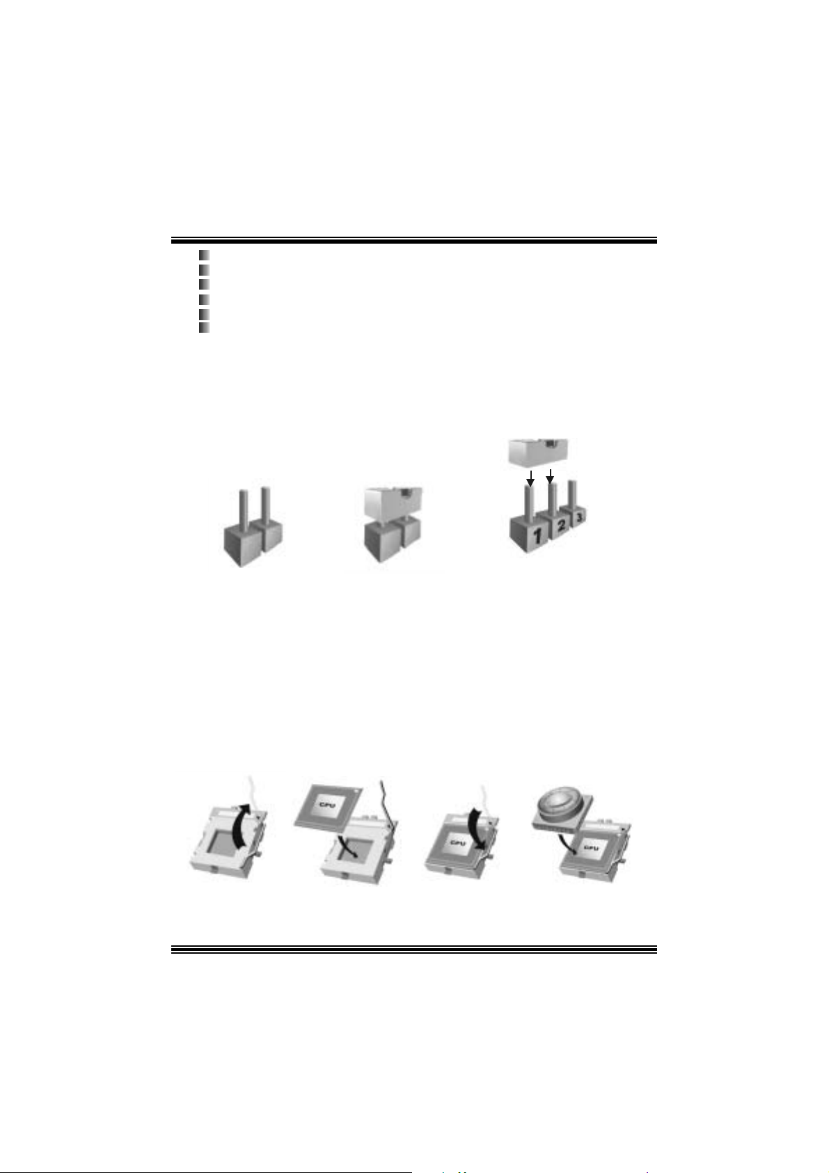
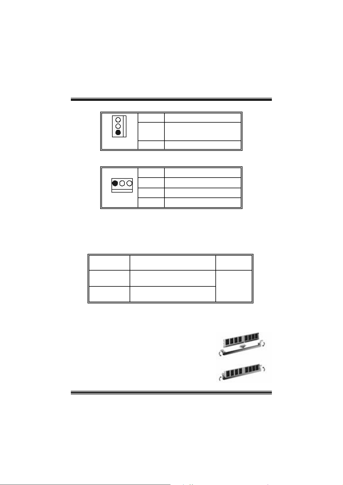
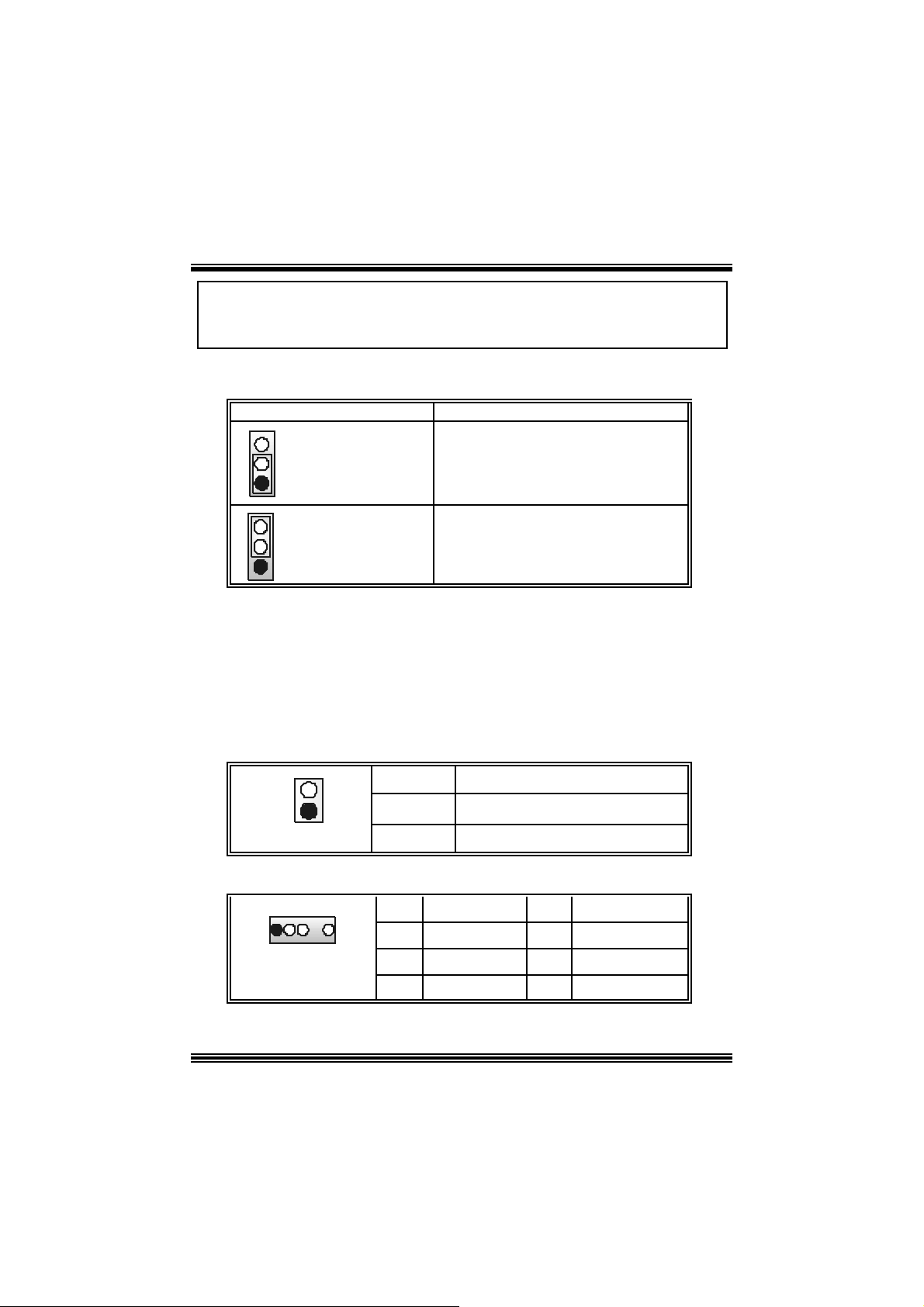
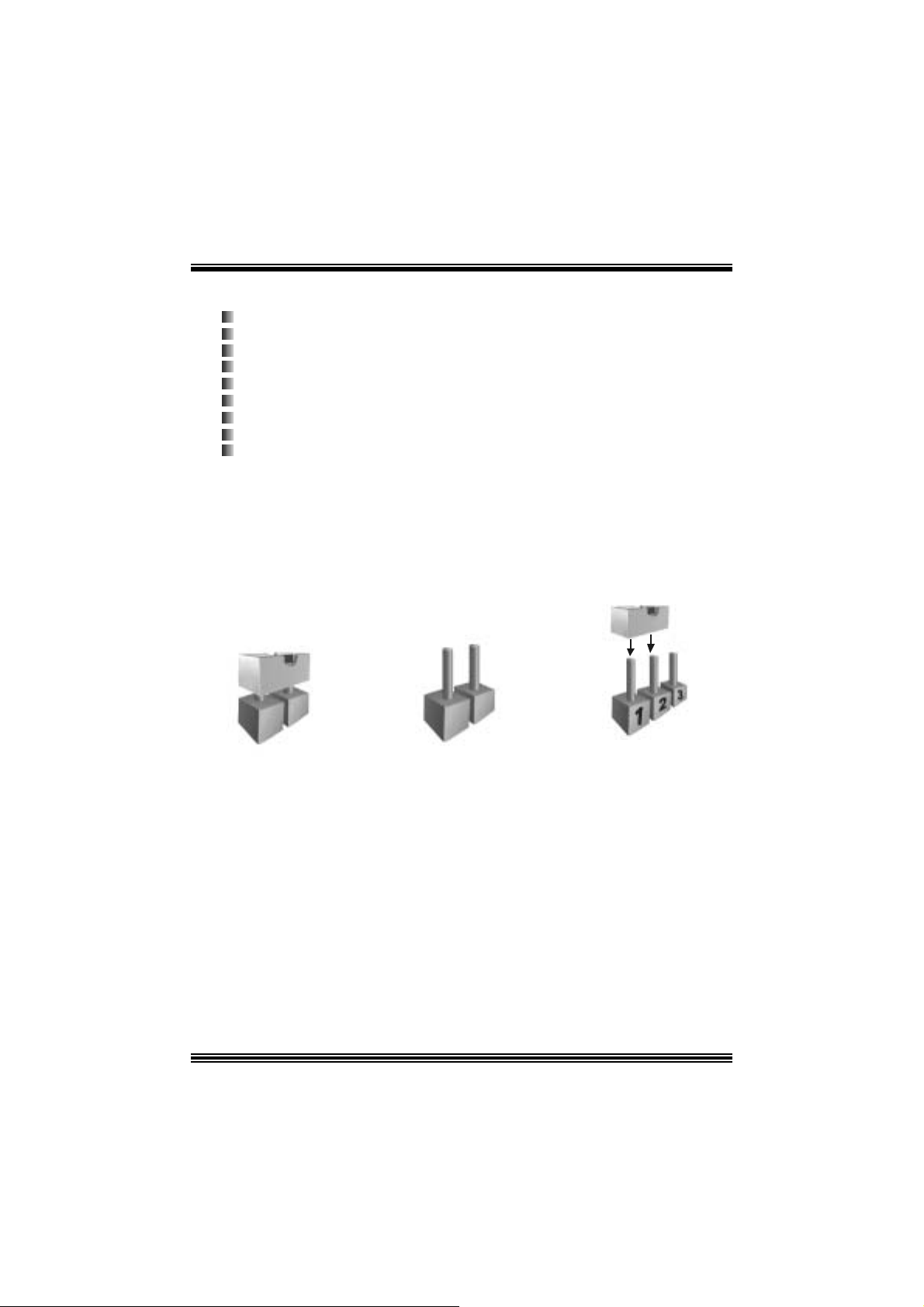
Ho w to set up a Jum pe r?
The illustration s hows how t o s et up jumpers. When a J umper c ap is placed on pins, t he
jumper is “close”. If no jumper cap is placed on the pins, the jumper is ”open”. The
illustration shows a 3-pin jumper whose pin1 and 2 are “close” when a jumper cap is
placed on thes e 2 pins.
Jumper open Jum per close Pin 1-2 close
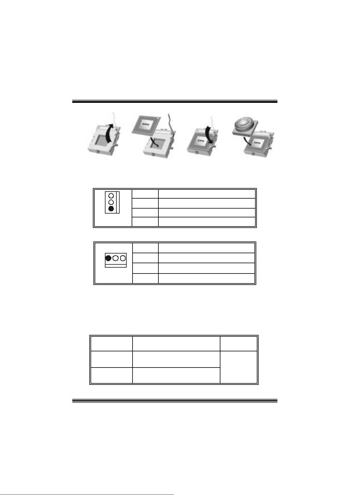
CPU Installation
Step1: Pull the lever sideway s away from the socket and then raise the lev er up to a
90 -degree angl e.
Step2: Look for the whit e dot /cut edge. The whit e dot/ cut edge should point wards the lever
piv ot. The C P U will f it only in the correct orient at ion .
Step3: Hold the CPU down fir mly, an d then cl ose the lever to complete the installation.
Step4: Put the CPU Fan on the C PU and buck le it. Connect the C PU fan power cable to
the JCFAN1. This completes the installation.
Ste p 1 Step2 Step3 Step4
6
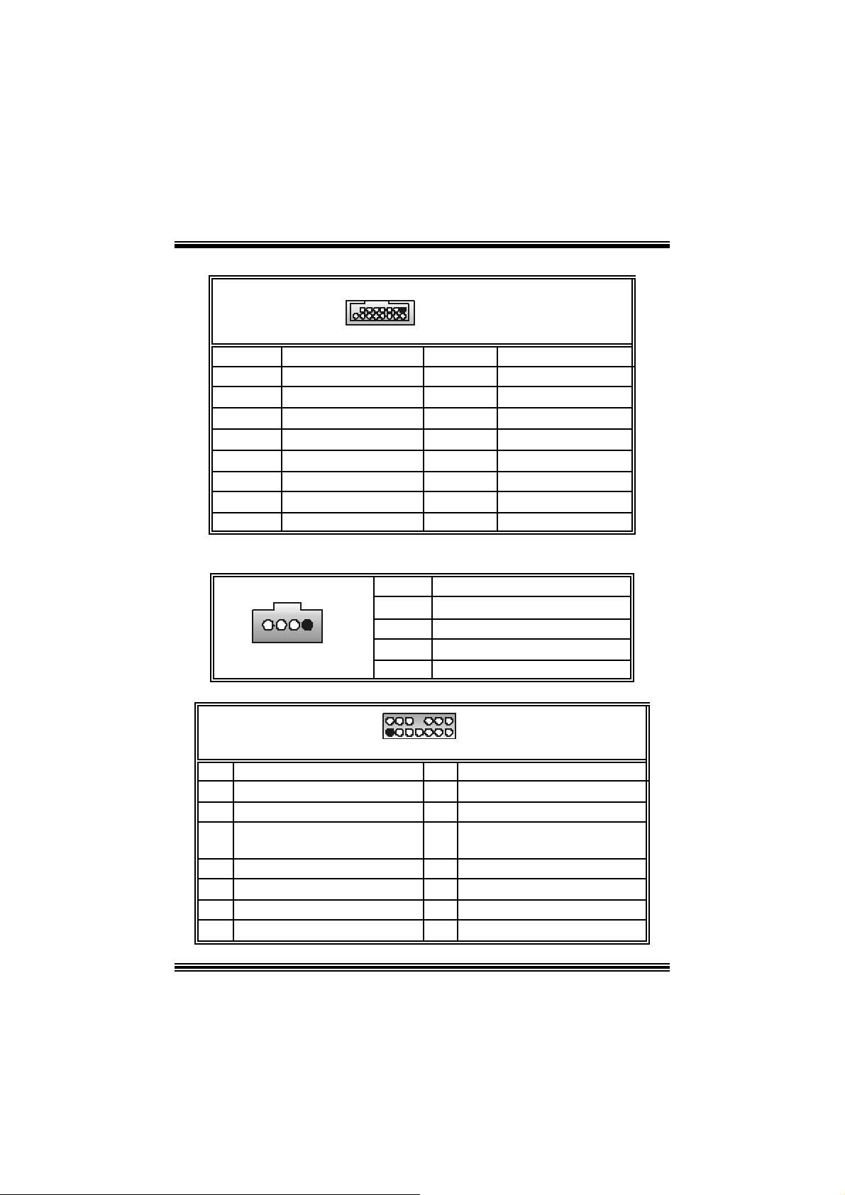
CPU Fan Header: JC FAN1
3
1
JCFAN1
Pin Assignment
1
2
3
Ground
+12V
FAN RPM rate Sense
S ystem Fan Header: JSFAN1
JSFAN1
Pin Assignment
1
31
2
3
FAN RPM rate Sense
Ground
+12V
DDR DI MM Module s: DDRA1/ DDRA2
DRAM Acces s Time: 2.5V Unbuffered/ no regis tered (without ECC) DD R SDRAM
PC2100/ PC 2700/ PC 3200 Type required.
DRAM Ty pe: 128MB/ 256MB/ 512MB/ 1GB DI MM Module. (184 pin)
DIMM Socke t
Location
DDRA1 6 4MB/128MB/256MB/512MB/1GB
DDRA2 6 4MB/128MB/256MB/512MB/1GB
DDR Mod u l e To tal Memory
Size (MB)
*1
*1
***O nly for referenc e***
Max is
2GB
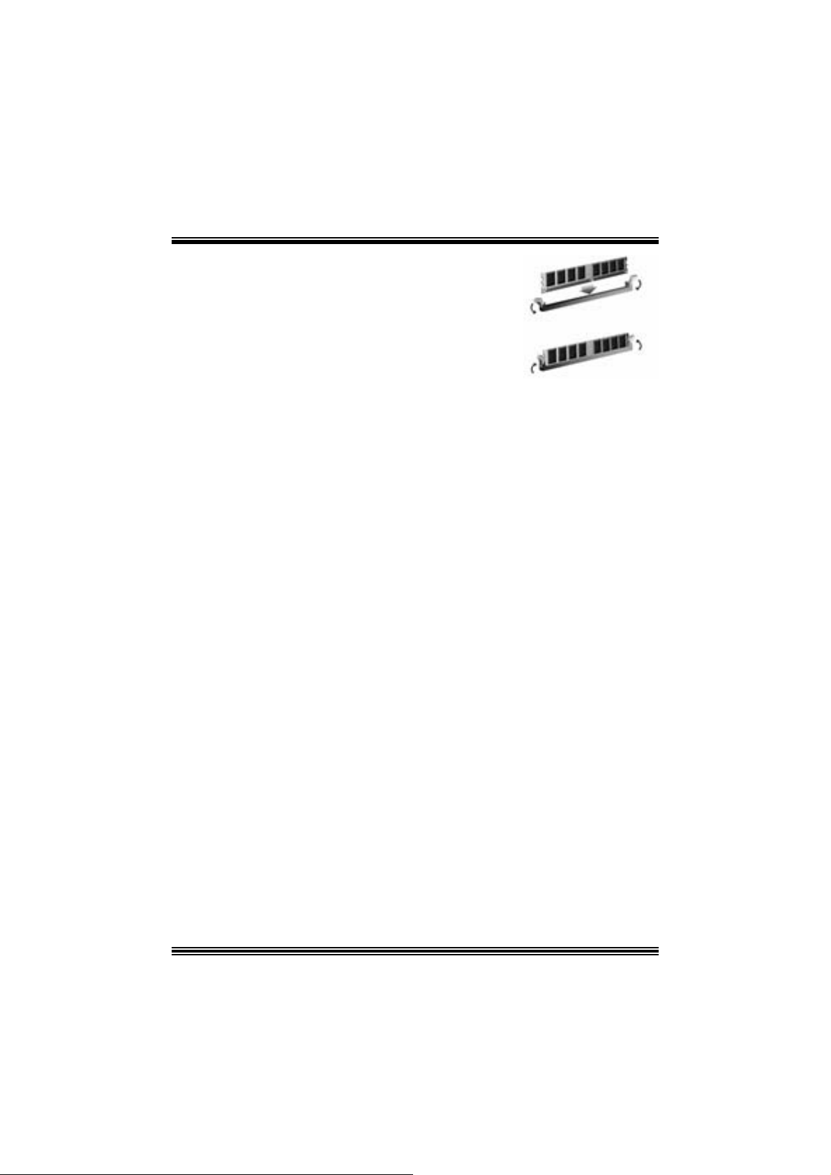
Installing DDR Mod ule
1. U nloc k a DIMM slot by press ing the retaining clips
outward. Align a DIMM to the slot in the way that
the notch of the DIMM mat ches t he break of the
slot.
2. I ns ert the DI MM vertically and firmly into the s lot
until the retaining chip snap back in place and the
DIMM i s properly seated.
7
Jump ers, H eade rs , Co nnectors & Slo ts
Floppy Disk Connector: FDD1
The mot herboard provides a standard f loppy disk connector that supports 360K,
720K, 1.2M, 1.44M and 2.88M floppy disk types. This connector supports the
prov ided f loppy drive ribbon cables .
Hard Disk Connectors: IDE1/ IDE2
The motherboard has a 32-bit Enhanced PCI IDE Controller that provides PIO
Mode 0~4, Bus Mast er, and U ltra DMA 33/ 66/ 100 f unctionality. I t has two H DD
connectors ID E1 (primary) and IDE2 (secondary).
The ID E c onnectors can c onnect a master and a slav e driv e, so y ou can c onnect
up to four hard disk drives . The f irst hard drive s hould alway s be c onnected t o
IDE1.
Peripheral Component Interconnect Slots: PCI 1-5
This m ot herboard is equipped with 5 st andard PCI s lots. PCI stands for Peripheral
Component I nterconnec t, and it is a bus standard for expansion cards. This PCI
slot is des ignated as 32 bits.
Accelerate d Graphics Port Slot: AGP1
Your monitor will attach directly to that video card. This motherboard supports
video cards f or PC I s lots, but it is als o equipped with an Accelerated Graphics Port
(AGP). An AGP c ard will take advantage of AGP technology f or improv ed video
efficiency and perform ance, es pecially with 3D graphics.
Communication Network Riser Slot: CNR1 (not su pport version
7.x)
The CNR specification is an open I ndust ry St andard Architecture, and it def ines a
ha rdw ar e scalable r iser card interfa ce, which su pports modem only.
S erial ATA C onnecto r: SATA1/ SAT A2
The mot herboard has a PCI to SATA C ontroller with 2 channels SATA interface, it
satisfi es t he SA T A 1. 0 s pec and wit h t r an s fer rat e of 1. 5Gb/s .
1234567
SATA1/ SATA2
Pin Assignment Pin Assignment
1
3
5
7
Ground
TXRX-
Ground
2
4
6
TX+
Ground
RX+
8
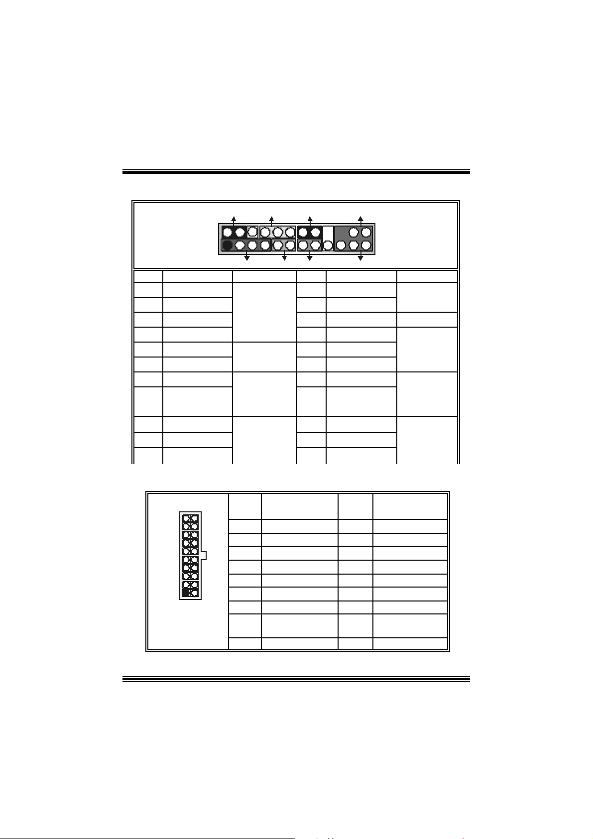
Front Pane l Conne ctor: JPANEL1
SLP
JPANEL1
2
123
Pin Assignment Function Pin Assignment Function
1 +5V 2 Sleep Control
3 NA 4 Ground
5 NA 6 NA NA
7 Speaker
9 HD D LED (+ ) 10 Powe r LED (+)
11 HDD LED (-)
13 Ground 14 Power Butt on
15 Reset Control
17 NA 18 KEY
19 NA 20 KEY
21 +5V 22 Ground
23 IRTX
PWR_LED
(+) (-)(+)
SPK
Connector
Hard Drive
Connector
(+) (-)
HLED
RST
Speaker
8 Power LED (+)
LED 12 Power LED (-)
Reset
Button 16 Ground
IrDA
24 IRR X
IRON/ OFF
IR
24
Sleep
Button
POWER
LED
Power-on
Button
IrDA
Connector
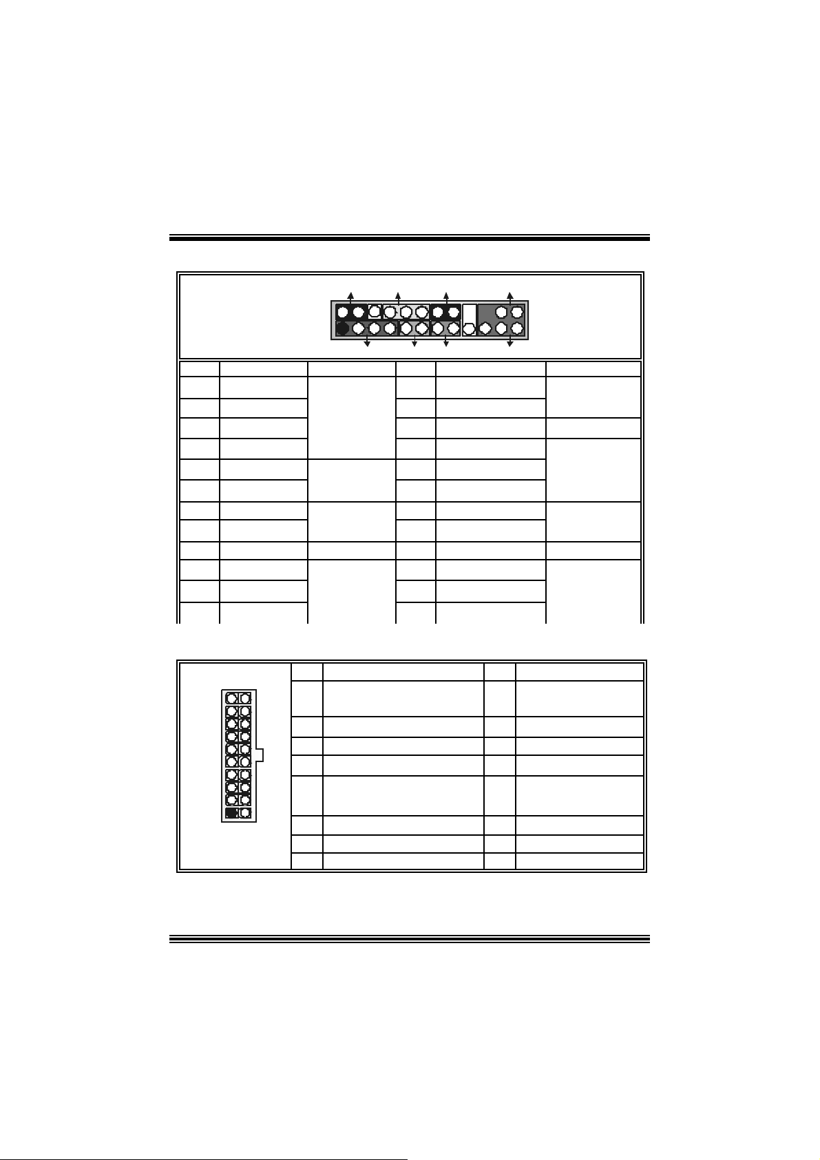
Power Conn ectors: JATXPWR1/ JATXPWR2
10
1
JATXPWR1
20
11
PIN Assignment PIN Assignment
1
2
3
4
5
6
7
8
9
10
+3.3V
+3.3V
Ground
+5 V
Ground
+5 V
Ground
PW_OK
Standby Volt age
+5 V
+1 2V
9
11
12
13
14
15
16
17
18
19
20
+3. 3V
-12V
Ground
PS_ON
Ground
Ground
Ground
-5V
+5V
+5V
1
1
3
2
JATXPWR2
PIN Assignment PIN Assignment
1
2
+12V
+12V
3
4
Ground
Ground
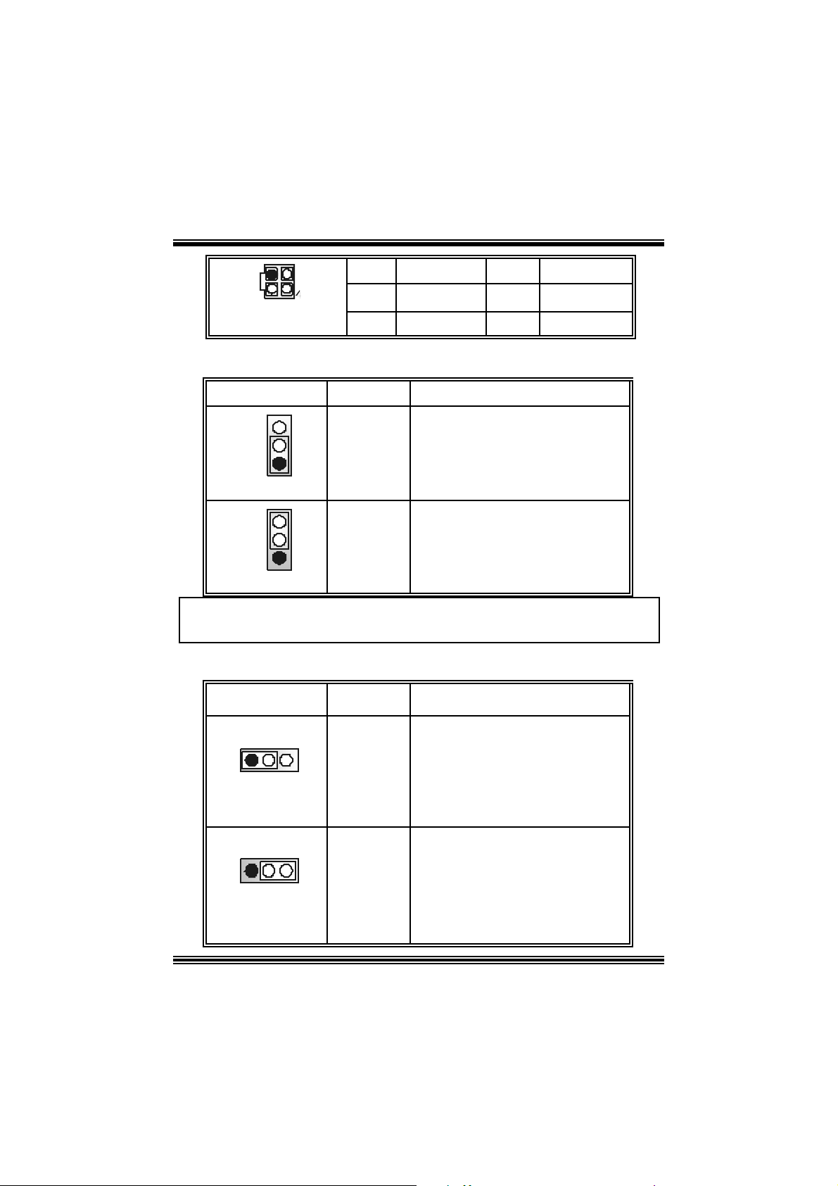
Power Source Selection for Keyboard/ Mouse: JKBV1 (only
optional on version 1.x)
JKBV1 Assignment Description
3
1
Pin 1-2 c los e
3
1
Pin 2-3 c los e
+5 V
+5V Standby
Voltage
+5V for keybo ard and mouse
PS/2 Mous e and PS/2 Key board are
powered with +5V standby v oltage
No t e: In o rder to su pport th i s fun cti o n “Pow e r-o n sy ste m v i a ke yb oa rd and
mouse”, “JKBV1” jumper cap should be placed on pin 2-3.
Power Source Selection for USB: JUSBV1/ JUSBV2/ JUSBV3_4
(only optional on version 1.x)
JUSBV1/JUSBV2/
JUSBV3_4
1 3
Pin 1-2 c los e
1 3
Pin 2-3 c los e
Assignment Description
+5 V
+5V Standby
Voltage
JUSBV1 : 5V for USB at th e JUSB1
connector port
JUSBV2: 5V f or USB at t he JRJ 45USB
coonector port
JUSBV3_4 : 5V for USB at the JUSB2/3
JU SBV1: JUSB1 port powered with
JU SBV2: JRJ 45USB1 port powered
JU SBV3_4: JUSB2/3 ports powered
10
connector ports
standby v olt age of 5V
with s t andby v olt age of 5V
with s t andby v olt age of 5V
Note: In order to support thi s function “Power-on system via USB devi ce”,
“JUSBV1/JUSBV2/ JUSBV3_4” jumper cap should be placed on pin 2-3
individually.
Clear CMOS Jumper: JCMOS1
JCMOS1 Assignment
3
1
3
1
Pi n 1-2 C lose
Pi n 2-3 C lose
Norm al Operation (def ault)
Clear CMOS Data
※ Clear CMOS Procedures:
1. R emov e AC power line.
2. Set the jumper to “Pin 2-3 C lose”.
3. Wa it for fi ve seconds.
4. Set the jumper to “Pin 1-2 C lose”.
5. Power on t he AC .
6. R eset your des ired password or clear t he C MOS dat a.
Ca se Op e n Connec to r: JCL1
Pin
1
JCL1
1
2
Assignment
Cas e Open Signal
Ground
AUDIO DJ Connector: JDJ1 (only optional on version 1.x)
15
JDJ1
Pin Assignment Pin Assignment
SMBDATA
1
3
5
INT_B
ATX_PWROK
2
4
SMBCLK
KEY
11
X
t
Game Header: JGAME1 (only optional on version 1.x)
15
Pin Assign m ent Pin Assignment
1
3
5
7
9
11
13
15
Joy stick B C oordinate X
Joy stick B C oordinate Y
+5V
Joy stick B Butt on 1
MIDI Output
Joy stick B Butt on 2
MIDI Input
NA
1
216
JGAME1
2
4
6
8
10
12
14
16
+5V
Joystick A Button 1
Joy st ick A Coordinate
Ground
Ground
Joy st ick A Coordinate Y
Joystick A Button 2
+5V
CD-ROM Audio-In Heade r: JCDIN1/ (JCDIN2: only optional
on version 1.x)
1
JCDIN1/ JCDIN2
Pin Assignment
1
2
3
4
Left Channel Inpu t
Ground
Ground
Right Channel Inp ut
Front Panel Audio Header: JAUDIO1
2
1
JAUDIO1
Pin Assignment Pin Assign m ent
1
3
5
7
Left Line Out/ Speaker Out Left
9
Right Line I n/ R ear Speaker R ight
11
Left Line In/ Rear Speaker Left
13
Mic In / C e nte r
Mic Power/ Bass
Right Line Out/ Speak er Out
Right
Reserv ed
12
14
13
2
4
Right Line Out/ Speaker Out Righ
6
8
Left Line Out/ Speaker Out Left
10
Right Line In/ R ear Speaker Right
12
Lef t Line I n/ Rear Speaker Left
14
Ground
Audio Power
Key
Digital Audio Connector: JSPDIF_OUT1 (optional )
1
JSPDI F_OUT1
Pin Assignment
1
2
3
+5V
SPDIF_OUT
Ground
Wake On LAN He ade r: WOL1 (only optional on version 1.x)
1
WOL1
Pin Assignment
1 +5V_Standby
2
3 Wake up
Ground
Front USB Header: JUSB2/JUSB3
9
10
JUSB2/3
Pin Assignment Pin Assignment
1
1
3
2
5
7
9
+5V
USB-
USB+
Ground
KEY
2
4
6
8
10
+5 V
USB-
USB+
Ground
NA
Auxiliary Audio-In C onnector: JAUX1 (only optional on version
7.x)
1
JAUX1
Pin Assignment
1
2
3
4
Left channel AUX_IN
CD_Ground
CD_Ground
Righ c hannel AUX_I N
S M Bus Cons ume r In frared Header: JS MB_C IR (onl y opti onal
on version 7.x)
8
7
12
JSMB_CI R
Pin Assignment Pin Assignment
1
3
5
7
Ground
CIRRX
NA
SMBDATA
13
2
4
6
8
+5V St andby
CIRTX
Power-on Butt on
SMBCLK
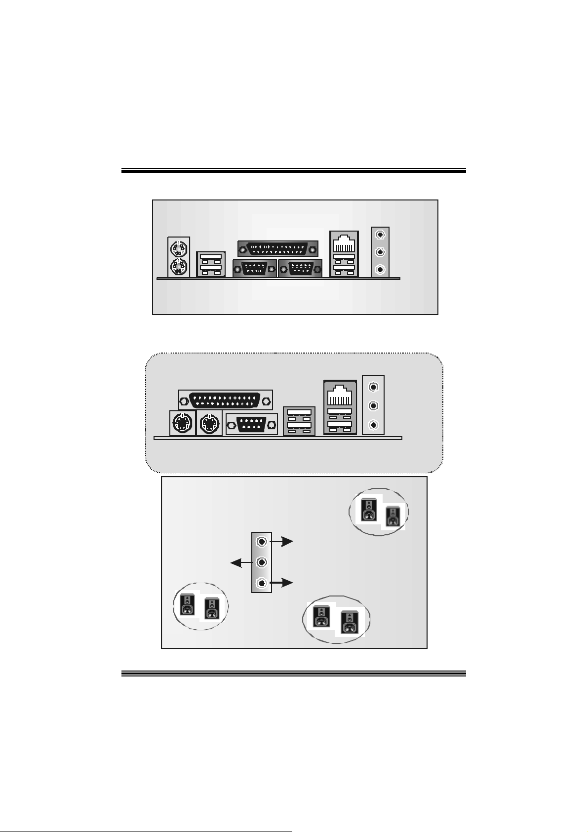
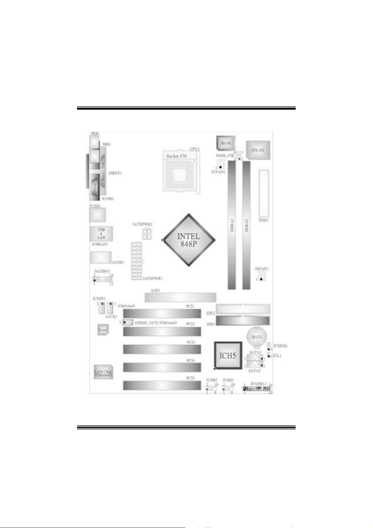
Back Pa nel Co nnectors (for version 1.x)
JKBMS1
PS/2
Mouse
PS/2
Keyboard
JUSB1
USB
Parallel Port
COM1
JCOM1
JPRNT1
JCOM2
JRJ45USB1
LAN
(optional)
COM2 USB
B ack Panel Connectors (for version 7.x)
Line In
Speaker Out
MIC In
JAUDIO
Pri nter Port
PS/2
Keyboard
PS / 2
Mouse
6 Channe l Speake rs
Speaker Out/
Right & Le ft
COM1
LAN
U SB
USB
(Optional)
Li n e In /
Rear Spea ker (Le ft & Right)
Mic In/ Center & Bass
Line In
Speak e r Out
Mic In
14

Deutsch
Die Spezifikationen von P4TSP-D2
A. Har dware
CPU
U terstüt zung für Sock el 478.
U nterstützung f ür Int el CPU Nort hwood. (Willamette wird nicht unterg es t ützt)
Unterstützung für den Intel Pentium® 4 Prozessor bis zu 3.2GH z.
Unterstützung für den Intel Pentium® 4 P r esc o t t C P U.
F SB mit 400/ 533/ 800MHz.
Uterstützung für die H yper-T hreading Technolo gi e.
Chipsatz
D ie Northbridge: Intel 848P.
D ie Southbridge: Intel ICH 5.
Hauptspeicher
U nterstüt zung für 64-bit Breite D DR-Dat enk anal mit ein oder zwei DIMMs pro
Kanal.
Verf ügbare Bandbreite bis zu 3. 2GB/s (DD R400) f ür Einzeln-Kanal-Modus.
U nterstüt zung für 128-MB, 256-Mb und 512-Mb DDR Tec hnologie.
Unt e r st ü t zung f ü r x8, x1 6 DDR Ger ä t e.
Vier DDR Speicherbänk e.
D ie m ax imale Speichergröße ist 2GB.
Super I/O
Chip: ITE IT 8712.
Low Pin C ount Int erface.
D ie m eisten gemeinsam en vergebraucht en Super I/ O Funktionen werden gelief ert.
Umweltkontroll-Initiative:
- H/W Monitor
- Vetilator-Geschwindigkeit-Controller
- I TE's "Smart Guardian" Funkt ion
Steckplätze
F ünf 32-bit PCI-Bus-Slots.
Ein C NR-Slot. (optional)
Ein 4X/ 8X AGP-Slot.
Onboard-IDE
Unterstützung fü r vi er IDE Diskettenl au fwe rke.
U nterstüt zung für PIO Modus 4, Ult ra DMA 33/ 66/100 Bus Master Modus.
LAN (optional)
15
Chip: RTL8 100C/ RTL8110S (B).
U nterstüt zung für 10 Mb/s, 100 Mb/ s und 1000Mb/s Auto-Negot iation.
Halb/Voll-Duple x Fä higkei t.
U nterstüt zung für ACPI, PCI Power Managem ent.
Onboard AC’97 Sound Codec
Chip: C MI9739A (für v ers ion 1. 0-12)/CMI 9761A (für v ersion 1.3 & v ersion 7.x ).
Ent s pricht der Spezif ikation von AC ’97.
AC 97 2. 2 Interf ace (CMI9739A)/ AC 97 2.3 Interf ace (CMI9761A).
Unterstützung für 6-Kanal.
Unterstützung für Stereo-Mikrof on (für CMI9761A).
Onboar d-Periph eriegeräte
a. R ü c kwan d
2 s erielle Sc hnittstellen. (1 s erielle Schnittstelle für version 7.x)
1 parallele Sc hnittstelle. (SPP/EPP/ECP-Modus )
Audio-Sc hnittst ellen auf der v ertikalen Posit ion.
1 R J -45 LAN Buc hse.(optional)
PS/ 2-Maus und PS/2-Tastatur.
4 USB2.0-Ports.
b. Vorder seit e
1 F loppy-Port m it Unterstützung f ür 2 Dis k et t enlauf werke.(360KB, 720KB, 1.2MB,
1.44MB und 2.88MB)
4 USB 2.0- P or ts .
1 Front- Audio-Head er.
1 S/PDIF-Header. (o ptional)
Abmessung
ATX F orm -Fac tor: 20.3 X 30.5c m (W X L)
ATX F orm -Fac tor: 20.3 X 30.5c m (W X L) (f ür v ersion 7. x)
B. BIOS & S oftware
BIOS
Award legal BI OS.
Unterstützung für APM1. 2.
Unterstützung ACPI.
Unterstütz ung USB Funkion.
Software
Unterstützung für Wa rps peede r ™, 9 th T ouch™, BootBlockerTM, WinFl as herTM,
FLASHER™
Unter stützung für die am meis ten ver breite ten Betriebsyst e me wi e Win d ows
98SE. , Windows 2000, Windows ME, Windows XP and SCO UNIX us w..
16
Verpack ungsinhalt
HDD Kable X 1
FDD Kable X 1
Benut zer Handbuch X1
Treiber C D für Installation X1
USB 2.0 Kable X1 (opt ional)
S/ PD IF Kable X 1 (optional)
I/O-R üc k wand für ATX Gehäuse X 1
Serial ATA Kable X 1 (opt ional)
Serial ATA N et zsc halter Kable X 1 (optional)
Ei nst e l lu ng de r Jum per
Die Abbildung verdeutlicht, wie Jumper eingestellt werden. Pins werden durch die
Jum per-Kappe v erdeckt, ist der Jum per ”geschlossen”. Keine Pins werden durch die
Jum per-Kappe verdeckt, is t der Jum per “geöffnet”. Die Abbiildung zeigt einen 3-Pin
Jumper dessen Pin1 und Pin2 ”geschlossen“ sind, bzw. es bef indet sich eine
Jum per-Kappe auf dies en beiden Pins.
Jumper geschlossen Jumper geöffnet Pin1-2 geschlossen
In stallat ion der CPU
Sc hritt 1 : Z iehen Sie den H ebel s eitlich vom Sockel weg. Heben Sie den Hebel dann
in 90-Grad-Winkel nac h oben.
Sc hritt 2 : Suchen Sie nac h der scharfen Kant e, die auf D rehpunkt des Hebels
weisen m uss . Die CPU passt nur, wenn s ie ric htig aus geric ht et ist.
Sc hritt 3 : D rück en Sie die CPU f est in den Sock el und s c hließ en Sie den Hebel.
Sc hritt 4 : St eck en S ie Ihr en C PU -Lüf t er auf die C PU . Schli eße n Sie die
Strom verso rgungsstecker für CPU-Lüfter an JCFAN1 an . Dann be enden
Sie die I nstallation.
17
Schritt 1 Schritt 2 Schritt 3 Schritt 4
CPU- Lüfter Header: JCFAN1
3
1
JCFAN1
Pin Beschreibung
1
2
3
Lüft er R PM Geschwindigk eit Sens or
Masse
+12V
System-Lüfter Header: JSFAN1
JSFAN1
Pin Beschreibung
1
31
2
3
Lüft er R PM Geschwindigk eit Sens or
Masse
+12V
DDR- DIMM-Mo dule s: DDRA1/ DDRA2
DRAM-Zugriffs zeit: 2.5V unbuf f ered/ nicht regist rierter (ohne EC C) DDR SDR AM
PC2100/ PC 2700/ PC 3200 Ty p erforderlich.
DRAM-Ty p: 128MB/ 256MB/ 512MB/ 1GB D I MM-Module (184-Pin)
DIMM-Sockel
Standort
DDRA1
DDRA2
64MB/128MB/256MB/512 MB/1G B
64MB/128MB/256MB/512 MB/1G B
DDR-Module Speichergröße
(MB)
*1
*1
***Nur als Referenz***
Ma ximal ist
2GB
18
In stallat ion von DDR-Modul
1. Öffnen Sie einen DIMM-Slots, indem Sie die
seitlich Chips nach außen drücken. Richten Sie
da s DIMM-Mo dul so über dem Slot aus , dass das
Modul mit der Kerbe in den Slot pas st.
2. D rücken Sie das DI MM-Modul in den Slot, bis die
seitlichen Clips zus chnappen und das Modul fes t
sitzt.
Jump ers, H eade rs, Anschlüs s e & S lot s
Diskettenanschluss: FDD1
Das Motherboard enthält einen st andardmäßigen Diskettenans chluss, der 360K-,
720K-, 1.2M-, 1.44M- und 2.88M-Disketten unterstützt. Dieser Anschluss
unt ers tützt die mit gelief erte Bandkabel des Diskettenlauf werks.
Fe stplatt enanschlüsse: IDE1 und ID E2
Das Mainboard hat einen 32-Bit Enhanced PCI IDE-Controller, der die Modi
PIO0~4, Bus Mast er sowie die U ltra DMA/33/ 66/100/133- Funkt ion zur Verfügung
stellt. Dieser ist mit zweii HDD-Anschlüssen versehen IDE1 (primär) und IDE2
(sekundär).
Die ID E-Anschlüsse k önnen eine Master- und eine Slav e-Festplatte v erbinden, so
dass bis zu 4 Festplatten angeschlossen werden können. Die erste Festplatte
sollte im m er an IDE1 angeschlossen werden.
Peripheral Component Interconnect Slots: PCI 1-5
Dieses Motherboard ist m it 5 standardmäß igen PCI-Slots ausgestattet. PC I steht
für Peripheral Component Interc onnect und bezieht sich auf einem Busst andard für
Erweiterungskarten, der den älteren ISA-Busstandard in den meisten
Schnittst ellen ers etzt hat. Dieser PCI-Slot ist f ür 32 bits v orgesehen.
Accelerate d Graphics Port Slot: AGP1
Ihr Monitor wird direkt an die Grafikkarte angeschlossen. Dieses Motherboard
unterstützt Grafikkarten f ür PCI-Slots, aber es ist auch mit einem Accelerated
Graphic s Port ausges tattet. AGP-Karten v erwenden die AGP-Technologie, um die
Wirks amk eit und Leistung v on Videosignalen zu v erbessern, besonders wenn es
sich um 3D-Graf iken handelt.
Commun ication Netwo rk Rise r Slot: CNR1 (op tiona l)
Die CNR-Angaben entsprechen einer off enen I ndustry Standard Archit ecture, und sie
definieren eine Hardware-skalierbare Riser-Card-Schnittstelle, welche nur Audio,
Netzwerk und Modem unterstützt.
Serial ATA Co nnector: JSATA1/JSATA2
Auf dies en Motherboard gibt es ein PCI -to-SATA C ont roller m it 2-Kanal Interfac e,
die der Spezifikation von SATA 1.0 ent spricht ( D t enübert ragung m it 1.5Gb/S)
19
Anschlüsse für die Vo rderseite: J PANEL1
PWR_LED
SLP
(+) (-)(+)
JPANEL 1
Pin Belegung Funktion Pin Belegung Funktion
1 +5V 2 Schlaf- Kont roll
3 Kein 4 Erde
5 Kein 6 Kein Kein
7 Lautsprecher
9 HDD LED (+) 10 P ower LED (+)
11 HDD LED (-)
13
15
17 Kein 18 Schlüsse
19
21
23
Masse
Re set-Kontroll
Kein
+5V
IRTX
224
123
(+) (-)
SPK
Lautsprecher-
Anschluss
Festplatte
LED 12 Power LED (-)
Rückstell-
knopf
IrDA-
Anschluss
HLED
RST
8 Power LED (+)
14
16 Erde
20
22 Erde
24
Power-Knopf
Schlüsse
IRR X
IRON/OFF
IR
Schlaf-
Knopf
POWER
LED
Power-On
Knopf
IrDA
Anschluss
Power Conn ectors: JATXPWR1/ JATXPWR2
10
1
JATXPW R1
PIN Belegung PIN Belegung
20
11
1
2
3 Erde 13
4
5 Erde 15 Erd e
6
7 Erde 17 Erd e
8
+5V reserv ierte Spannung
9
10
+3.3V
+3.3V
+5V
+5V
PW_OK
+12V
11
12
14
16 Erd e
18
19
20
+3.3V
-12V
Masse
PS_ON
-5V
+5V
+5V
20
 Loading...