


LCD COLOUR TV
SERVICE MANUAL
CHASSIS NO.: LS01
Please read this manual carefully before service.
1
Catalog |
|
Chapter 1: Specifications and Composition................................................................................................. |
3 |
2. Function introduction of ICs or functional module of LCD TV with LS01chassis............................... |
8 |
Chapter 3: Analysis of Signal process Flowchart and key point measure date..................................... |
31 |
Chapter 4: Maintenance Procedure and Examples of Typical troubleshooting........................................ |
43 |
Chapter 5: Spare Part Lists.......................................................................................................................... |
44 |
Chapter 6: Factory Setup and notice........................................................................................................... |
45 |
Appendix: 1. Circuit Schematic diagram
2.Circuit Schematic diagram of power module
3.Final Assembly diagram
4.Wiring diagram of LCD TV with LS01 chassis (take LT32GJ01E as an example)
2

Chapter 1: Specifications and Composition
1. Models for LS01 chassis :
Region |
Europe |
America |
Other regions |
|||
Original |
LT26GJ01E |
LT32GJ01E |
LT26GJ01U |
LT32GJ01U |
LT26GJ01A |
LT32GJ01A |
Models |
LT37GJ01E |
LT26GJ12E |
LT37GJ01U |
LT26GJ12U |
LT37GJ01A |
LT26GJ12A |
|
LT32GJ12E |
LT37GJ12E |
LT32GJ12U |
LT37GJ12U |
LT32GJ12A |
LT37GJ12A |
|
LT26GJ88E |
LT32GJ88E |
LT26GJ88U |
LT32GJ88U |
LT26GJ88A |
LT32GJ88A |
|
LT37GJ88E |
|
LT37GJ88U |
|
LT37GJ88A |
|
2. Main Feature
Region |
Europe |
|
America |
|
Other regions |
RF signal Color |
PAL SECAM |
|
NTSC PAL M PAL N |
PAL NTSC SECAM |
|
system |
|
|
|
|
|
Sound |
D/K B/G I L/L’ |
M |
|
D/K B/G I M |
|
system |
|
|
|
|
|
Video or Y/C signal |
PAL NTSC SECAM |
PAL NTSC SECAM |
PAL NTSC SECAM |
||
Program presetting |
100 0-99 |
|
68 AIR 2-69 |
|
236 0-235 |
|
|
|
125 CABLE 1-125 |
|
|
Audio |
5W+5W |
|
5W+5W |
|
5W+5W |
output THD≤7% |
|
|
|
|
|
Power source |
100V 240V |
|
100V 240V |
|
100V 240V |
Teletxt |
100 pages |
|
X |
|
100 pages |
CCD |
X |
|
Yes |
|
X |
Sound demodulator |
NICAM IGR |
|
BTSC |
|
NICAM IGR |
SCART |
Yes |
|
X |
|
X |
VGA |
Yes |
|
Yes |
|
Yes |
YPbPr |
Yes |
|
Yes |
|
Yes |
HDMI |
Yes |
|
Yes |
|
Yes |
Earphone |
Yes |
|
Yes |
|
Yes |
OSD language |
English, |
French, |
English, |
French, |
English, French, German, |
|
German, |
Italian, |
Portuguese, Spanish etc. |
Spanish etc. |
|
|
Portuguese etc. |
|
|
|
|
Auto Off without Signal |
5 minutes |
|
|
|
|
Reception |
|
|
|
|
|
Program booking |
5 program booking. Turn to the corresponding program at the booking time. |
||||
Swap |
Customer could rearrange the channels according to personal habit |
||||
Energy saving system |
Customer could adjust LCD screen backlight brightness manually to save energy. |
||||
Plug and Play |
LCD TV could be used as computer screen, no need for the installation of software, |
||||
|
which is Plug and Play in real sense |
|
|
||
3
3. Unit IC Compositions
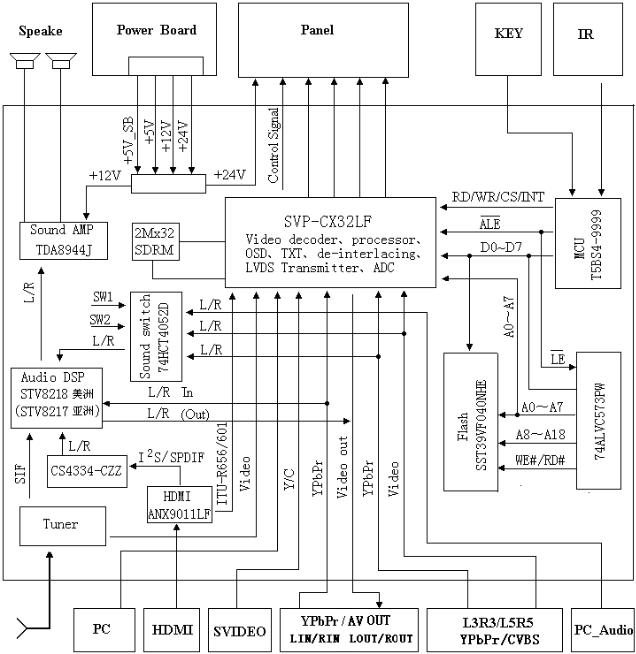
LCD TV with LS01 chassis is made up of switch power, system control circuit, video processing circuit, audio processing circuit, Power Amplifier circuit, AV input circuit, LCD screen module. Block circuit diagram is shown as below:
1) European market:
4

2). American and Asian market:
5
6

4. Introduction of PCB module
LCD TV with LS01 is made up of power board, side AV board, remote control reception board, key board, and mainboard. The table below is the introduction of the function of all printed board modules.
No. |
Parts |
Description |
1 Mainboard |
Mainboard module is the core of LCD TV signal processing. Under the |
|
|
module |
control of the system control circuit, It undertakes the task of converting the |
|
|
external input signal into the unified digital signal that the LCD screen could |
|
|
identify. Mainboard controls the whole machine through IIC bus, decode |
|
|
VIDEO signal, controls the Video (brightness, contrast, chroma, hue, |
|
|
definition etc), white balance adjusts, generates OSD, de-interlaces signal, |
|
|
converts signal frequency, and finishes signal A/D and D/A conversion, video |
|
|
enhancement, LVDS signal coding and output; it has Scart , S-Video, AV , |
|
|
YPbPr, HDMI and PC interface, Tuner input, sound demodulation, sound |
|
|
processing, sound power amplifier, and online update. |
2 Remote |
The remote reception board module is constituted by an indicator-light and a |
|
|
reception |
remote reception. Customer could manipulate the LCD TV by using remote |
|
module |
controller very conveniently. By the color of the indicator light, the operation |
|
|
mode of the LCD TV could be judged (red is standby, green is power on). |
3Built-in powerConvert the 100V 240V 50/60HZ AC into DC, output have +24v, +12V, board module +5V, and the +5V_STB in standby state.
4 |
Keyboard |
Keyboard module has 7 function keys (program +/-, volume +/-, AV/TV, |
|
module |
menu ,power), customer could use the key to operate the TV freely. |
5 |
LCD screenLCD screen has built-in inverter that convert DC into high voltage AC signal |
|
|
module |
to turn on the backlight CCFL (Cold Cathode Fluorescent Light); the LCD |
|
|
screen process the video signal from signal board and reappear. |
6 |
Side |
AVSide AV board is used for earphone output. |
|
board |
|
7

Chapter 2: Function Introduction of Main IC
1. Main ICs and functional modules of LS01 chassis
No. |
Item no. |
Model |
Main function |
1 |
U15 |
JS-6H2/121 |
Tuner output sound IF and video signal |
2 |
U1 |
SVP-CX32LF |
Video decoder, image processor, A/D and D/A |
|
|
|
conversion |
3 |
U2 |
IS42S32200C1-6TL |
SDRAM with 2MX32bits |
4 |
U3 |
AT24C64A-10PU-2.7 |
EEPROM |
5 |
U4 |
T5BS4-9999 |
MCU |
6 |
U5 |
SST39VF040-70-4C-NHE |
Flash, Store the Control program. |
7 |
U6 |
74ALVC573PW |
Address latch, to latch the address wires |
8 |
U8 |
TCM809SENB713 |
Hardware reset IC of MCU |
9 |
U9 |
74HCT4052D |
Audio input switch of AV terminal |
10 |
U35 |
STV-8217/STV-8218 |
Audio signal processor |
11 |
U14 |
74LVC14AD |
VGA line and field synchronizing signal waveform |
|
|
|
shaping |
12 |
U16 U25 |
AT24C02BN-10SU-1.8 |
EEPROM |
14 |
U18 U22 |
AZ1117H -1.8TRE1 |
3.3V to 1.8V DC conversion |
16 |
U19 U24 |
AZ1117H -3.3TRE1 |
5V to 3.3V DC conversion |
18 |
U20 |
AZ1084S -3.3TRE1 |
5V to 3.3V DC conversion |
19 |
U21 |
AZ1084S -1.8TRE1 |
5V to 1.8V DC conversion |
20 |
U23 |
AZ78L08ZTR-E1 |
12V to 8V DC conversion |
21 |
U26 |
CS4344-CZZ |
HDMI digital audio decode, DAC |
22 |
U28 U29 |
Rclamp0514M.TBT |
ESD protection device of HDMI |
24 |
U30 |
ANX9011L |
HDMI digital signal decode |
25 |
U31 |
PI5C3306LE |
(SDA, SCL) used for program update |
26 |
U33 |
TDA8944J |
Audio amplifier (BTL output) |
2. Function introduction of ICs or functional module of LCD TV with LS01chassis
8

1.Tuner (JS-6H2/121 or CDT-6GPL22-00) |
|
|
Pin No. |
Definition of pin |
Function description |
1 |
NC |
No connection |
2 |
BT |
No connection |
3 |
VCC |
+5V power |
4 |
SCL |
IIC bus (clock) |
5 |
SDA |
IIC bus (data) |
6 |
AS |
Ground |
7 |
AFS |
Ground |
8 |
NC |
No connection |
9 |
NC |
No connection |
10 |
NC |
No connection |
11 |
SIF/Out |
Sound intermediate Frequency output |
12 |
Video/Out |
CVBS signal output |
13 |
VCC +5V |
+5V power |
14 |
Audio/Out |
Audio signal output |
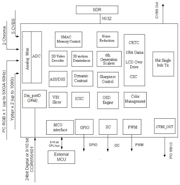
2. Image processing IC SVP-CX32LF
The SVPTMCX video processor is a highly integrated system-on-a-chip device, targeting the converging HDTVready and PC-ready LCD TV, PDP TV applications where high precision processing of video and data are the requirements. SVPTMCX contains 6th generation dualpurposed triple 10-bit high-precision and high speed video ADCs for both PC and video inputs, the high-performance multi-format 3D digital comb video decoder that supports NTSC, PAL, and SECAM*, a HDTV sync separator, motion adaptive de-interlacing engine, and the video format conversion engine, supporting multi-window display in many different output modes. Trident’s DCReTM – Digital Cinema Reality engine, is integrated inside the SVPTMCX family to provide the most natural cinema-realistic images. The DCReTM technology integrates advanced 3D-comb video decoding, advanced motion adaptive de-interlacing, object-based digital noise reduction, advanced 6th generation scaler, film mode support, average picture level (APL), edge smoothing and dynamic sharpness enhancement. Trident's patented Unified Memory Architecture (UMA) that allows frame rate conversion, 3D comb video decoding, and video enhancement processing to share the same memory buffer that is made up of highspeed and cost-effective PC graphic memory. All these advanced digital processing techniques combined with a true 10-bit video data processing for the most optimal video fidelity to provide the most natural and cinema quality video images. Designed for maximum system design flexibility, SVPTMCX integrates all video interfaces to support converging digital video, analog video, and PC data applications. The users of Trident's single chip SVP™CX series video processor(s) will benefit from many features while maintaining a price competitive advantage over the existing solution(s)
9
Main features:
●Integrated 6th Generation Motion and Edge Adaptive De-interlacing
●Integrated ADC
●PC auto tune
●Built-in 8-bit LVDS Transmitter
●6th generation cubic-4 image scaling engine
●Advanced Chroma Processing and Dynamic Contrast Function
●Green color stretch, blue color stretch, skin color enhancement
●Integrated 6th Generation Motion Adaptive 3D Digital Comb Video Decoder with Programmable Filter
●60Hz 100Hz interlaced scanning and 50Hz 75Hz progressive scanning
●frame rate conversion
●14D dynamic picture enhancements
●Advanced Film Mode Recovery-3:2/2:2 pull down
●Build-in A/D conversion function
●Teletext function
●Supports 16/32bits SDRAM memory interface
●Multi-screen display mode
●OSD and VBI/Closed caption and advanced OSD engine Pin function description:
Pin No. |
Designation of pin |
Function of pin |
Analog signal input/output terminal |
|
|
169 |
CVBS1 |
CVBS input 1 |
180 |
Y_G1 |
Y input |
181 |
Y_G2 |
SCART1 Green signal input |
182 |
Y_G3 |
S-Video Y signal input |
183 |
PC_G |
PC Green signal input |
188 |
PR_R1 |
DVD interface Pr signal input |
189 |
PR_R2 |
SCART1 Red signal input |
190 |
PR_R3 |
SCART2 Y signal input |
191 |
PC_R |
PC Red signal input |
192 |
C |
S-Video C signal input |
196 |
PB_B1 |
DVD interface Pb signal input |
197 |
PB_B2 |
SCART1 Blue signal input |
198 |
PB_B3 |
SCART1 CVBS signal input |
199 |
PC_B |
PC blue signal input |
171 |
FS1 |
No connection |
170 |
FS2 |
No connection |
173 |
FB1 |
SCART1 RGB_FB signal input |
172 |
FB2 |
SCART2 chroma signal input |
174 |
VREFP_1 |
A/D conversion1 voltage reference + |
175 |
VREFN_1 |
A/D conversion 1 voltage reference - |
10
184 |
VREFP_2 |
A/D conversion 2 voltage reference + |
185 |
VREFN_1 |
A/D conversion 2 voltage reference - |
Digital signal terminal |
|
|
37 |
DP0 |
Digital signal I/O DP0~DP23 interface |
|
|
|
29 |
DP8 |
|
26 |
DP9 |
|
25 |
DP10 |
|
24 |
DP11 |
|
22 |
DP12 |
|
21 |
DP13 |
|
18 |
DP14 |
|
|
|
|
14 |
DP18 |
|
11 |
DP19 |
|
|
|
|
7 |
DP23 |
|
CPU control terminal |
|
|
55 |
PWMO |
Pulse width modulation input |
57 |
SCL |
IIC clock |
58 |
SDA |
IIC data |
60 |
GPIO0 |
GPIO1 selection signal |
59 |
GPIO1 |
GPIO2 selection signal |
62 |
WR# |
CPU write signal |
63 |
RD# |
CPU read signal |
61 |
CS |
CPU chip selection signal low level effective |
56 |
INTN |
Interrupt signal low level effective |
84 |
ALE |
Address latch signal |
86 |
RESET |
Reset signal (high level effective) |
85 |
V5SF |
SF Power +5V |
4 |
DP_HS |
Line synchronization signal |
5 |
DP_VS |
Field synchronization signal |
23 |
DP_CLK |
Digital port Clock |
6 |
DP_DE_FLD |
DE I/O terminal |
64 |
ADDR0 |
CPU address R0~R7 signal |
|
|
|
71 |
ADDR7 |
|
83 |
A_D0 |
CPU address/data passage |
|
|
|
76 |
A_D7 |
|
MISC port control signal |
|
|
162 |
CVBS_OUT2 |
SCART2 interface CVBS signal output |
11
163 |
CVBS_OUT1 |
SCART1 interface CVBS signal output |
157 |
TEST MODE |
Test mode signal (grounding) |
158 |
AIN_HS |
Line synchronization signal |
159 |
AIN_VS |
Field synchronization signal |
205 |
XTALI |
Crystal oscillator interface |
204 |
XTALO |
|
SDRM |
|
|
124 |
MA0 |
Memory address A0~A11 |
|
|
|
121 |
MA3 |
|
118 |
MA4 |
|
|
|
|
113 |
MA9 |
|
125 |
MA10 |
|
126 |
MA11 |
|
156 |
DQM0 |
Memory read/write byte signal |
133 |
DQM1 |
|
109 |
DQM2 |
|
87 |
DQM3 |
|
128 |
BA0 |
Memory stack address selection |
127 |
BA1 |
|
130 |
RAS# |
RAS signal |
131 |
CAS# |
CAS signal |
132 |
WE# |
Memory write pulse |
112 |
CLKE |
Memory clock pulse |
129 |
CS0# |
Memory chip selection signal |
111 |
MCK |
Memory clock signal |
155 |
MD0 |
Memory data interface |
|
|
|
148 |
MD7 |
|
145 |
MD8 |
|
|
|
|
138 |
MD15 |
|
107 |
MD16 |
|
|
|
|
100 |
MD23 |
|
95 |
MD24 |
|
|
|
|
88 |
MD31 |
|
LVDS port |
|
|
52 |
LVDS_VDDP |
Power for LVDS |
38 |
PLL_GND |
PLL ground |
12

39 |
PLL_VCC |
PLL power |
47 |
LVDSGND |
LVDS ground |
46 |
LVDSVCC |
Power for LVDS |
43 |
TCLK1M |
Positive/Negative LVDS differential clock output |
42 |
TCLK1P |
|
51 |
TA1 M |
Positive/Negative LVDS differential data output |
50 |
TA1P |
|
49 |
TB1M |
|
48 |
TB1P |
|
45 |
TC1M |
|
44 |
TC1P |
|
41 |
TD1M |
|
40 |
TD1P |
|
Clock and power |
|
|
146 |
VDDM |
Memory port digital power |
134 |
VDDM |
|
108 |
VDDM |
|
98 |
VDDM |
|
72 |
VDDH |
3.3V power supply |
19 |
VDDH |
|
160 |
VDDC |
1.8V power supply |
136 |
VDDC |
|
119 |
VDDC |
|
96 |
VDDC |
|
74 |
VDDC |
|
53 |
VDDC |
|
27 |
VDDC |
|
12 |
VDDC |
|
13 |
VSSC |
Digital ground |
28 |
VSSC |
|
54 |
VSSC |
|
75 |
VSSC |
|
97 |
VSSC |
|
120 |
VSSC |
|
137 |
VSSC |
|
161 |
VSSC |
|
20 |
VSSH |
|
73 |
VSSH |
|
99 |
VSSM |
|
110 |
VSSM |
|
135 |
VSSM |
|
147 |
VSSM |
|
13

195 |
AVDD3_ADC2 |
ADC analog power (+3.3V) |
168 |
AVDD3_ADC1 |
|
2 |
PLF2 |
Video PLL clock low pass filtering |
207 |
MLF1 |
Memory PLL clock low pass filtering |
1 |
PAVSS2 |
PLL ground |
3 |
PAVDD2 |
PLL power (+1.8V) |
206 |
PAVSS1 |
PLL digital ground |
208 |
PAVDD1 |
PLL digital ground power (+1.8V) |
203 |
PAVSS |
PLL Digital ground |
202 |
PAVDD |
PLL digital ground power(+1.8V) |
201 |
PDVSS |
PLL Digital ground |
200 |
PDVDD |
PLL digital ground power (+1.8V) |
177 |
AVDD_ADC1 |
ADC analog power (+1.8V) |
186 |
AVDD_ADC2 |
|
193 |
AVDD_ADC3 |
|
178 |
AVDD_ADC4 |
|
176 |
AVSS_ADC1 |
ADC analog ground |
187 |
AVSS_ADC2 |
|
194 |
AVSS_ADC3 |
|
179 |
AVSS_ADC4 |
|
165 |
AVDD3_OUTBUF |
+3.3V analog power |
164 |
AVSS_OUTBUF |
|
166 |
AVDD3_BG_ASS |
Analog ground |
167 |
AVSS_BG_ASS |
|
SVP-CX32LF internal block diagram:
14
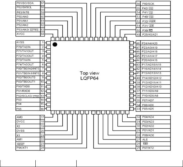
3 T5BS4-9999 brief introduction:
T5BS4-9999 is a high-speed 16-bit micro-controller designed for the control of various mid-
to
large-scale equipment. T5BS4-9999 is ROM-less product, T5BS4-9999 comes in a 64-pin flat package. Listed below are the features that is used for the control of a variety of small to large devices. T5BS4-9999 could extend ROM ,64 pins and is packaged in PLCC. It is the main control IC of the TV via I²C bus.
Main features:
●High speed 16-bit CPU 900/L1 CPU
●Minimum instruction execution time: 148ns
●Build-in RAM: 10Kbytes
●Expandable up to 16Mbytes
●simultaneously support 8-/16-bit width external data bus
15
●8-bit timers: 6 channels, 16-bit timers: 1 channel ●General-purpose serial interface: 1 channel ●Serial bus interface: 1 channel
●10 bit A/D conversion interface: 4 channels ●Watchdog timer
●Timer for real time clock (RTC)
●Chip select/wait controller: 4 blocks
●34 interrupt signals output
9 CPU interrupt, 21 internal interrupt, 4 external interrupt
●53 I/O pins
●Standby function
●Clock control
fs=32.768KHz real-time time of time conversion function high frequency fc to fc/16 ● Working voltage
When fc=27 MHZ, VCC=2.7~3.6V, when fc=10MHZ, VCC=1.8V to 3.6V ● 64 pin package P-LQFP64-1010-0.50D standard
Pin assignment description:
Pin introduction: |
|
|
Pin |
Designation |
Function description |
16

1 |
AVSS |
Analog ground |
2 |
P70/TA0IN |
I²C data input |
3 |
P71/TA1OUT |
I²C clock output |
4 |
P72/TA3OUT |
PAGE signal output |
5 |
P73/TA4IN |
+5V power |
6 |
P74/TA5OUT |
Backlight on/off control |
7 |
P80/TB0IN0/INT5 |
Remote control signal |
8 |
P81/TB0IN1/INT6 |
+1.8V power supply |
9 |
P82/TB0OUT0 |
Remote red control signal |
10 |
P83/TB0OUT1 |
Remote green control signal |
11 |
P90/TXD0 |
Digital ground |
12 |
P91/RXD0 |
HDMI identity signal |
13 |
P92/SCLK0/ |
No connection |
14 |
P93 |
CON4(10th pin) |
15 |
P94 |
CON4(4th pin) |
16 |
P95 |
CON4(3rd pin) |
17 |
AM0 |
Bus byte selection |
18 |
DVCC |
+3.3V power |
19 |
X2 |
Crystal oscillator interface |
20 |
DVSS |
Ground |
21 |
X1 |
Crystal oscillator interface |
22 |
AM1 |
Bus byte selection |
23 |
|
CPU reset control port |
24 |
P96/XT1 |
Low frequency oscillation input interface |
25 |
P97/XT2 |
Low frequency oscillation output interface |
26 |
NMI |
Interrupt request signal |
27 |
ALE |
Address latch pulse |
28 |
P00/AD0 |
0~7 bit address/data port |
|
|
|
35 |
P07/AD7 |
|
36 |
P10/AD8/A8 |
8~15 bit address/data port |
|
|
or 8~15 bit address port |
43 |
P17/AD15/A15 |
|
44 |
P20/A0/A16 |
8~5 bit address port |
|
|
or 8~21 bit address port |
49 |
P25/A5/A21 |
|
50 |
P30/ |
External memory read control terminal |
51 |
P31/ |
External memory write control terminal (AD0~AD7) |
52 |
P32/ |
Data write control terminal (AD8~AD15) |
53 |
P40/ |
Internal address selection signal |
54 |
P41/ |
|
17

55 |
P42/ |
|
56 |
P60/SCK |
(no connection) |
57 |
P61/SO/SDA |
I²C data |
58 |
P62/SI/SCL |
I²C clock |
59 |
P63/INT0 |
Interrupt request signal |
60 |
P50/AN0 |
KEY signal port |
61 |
P51/AN1 |
|
62 |
P52/AN2 |
SCART1 FS signal |
63 |
P53/AN3/ |
SCART2 FS signal |
64 |
AVCC |
Analog power +3.3V |
T5BS4-9999 internal functional block diagram
18
 Loading...