


ACOUSTIC EFFECTS PROCESSOR BASS EFFECTS PROCESSOR GUITAR EFFECTS PROCESSOR
UB99A/UB99B/UB99MK2
SERVICE MANUAL
UB99A |
UB99B |
UB99MK2 |
ACOUSTIC EFFECTS PROCESSOR |
BASS EFFECTS PROCESSOR |
GUITAR EFFECTS PROCESSOR |
■ CONTENTS |
|
SPECIFICATIONS .......................................................... |
3 |
PANEL LAYOUT .............................................. |
4 |
BLOCK DIAGRAM .................................... |
5 |
CIRCUIT BOARD LAYOUT .......................... |
6 |
DISASSEMBLY PROCEDURES .................................... |
6 |
LSI PIN DESCRIPTION LSI ........................................ |
8 |
IC BLOCK DIAGRAM IC ........................................... |
11 |
CIRCUIT BOARD .................................................. |
12 |
INSPECTIONS / FACTORY SET / ..... |
14 |
BACKUP THE USER PATCH DATA |
|
.................................................... |
25 |
ERROR MESSAGES ..................................... |
26 |
PARTS LIST |
|
CIRCUIT DIAGRAM |
|
GA 011755
HAMAMATSU, JAPAN
Copyright (c) Yamaha Corporation. All rights reserved. PDF-K366 


 ’05.03

UB99A/UB99B/UB99MK2
IMPORTANT NOTICE
This manual has been provided for the use of authorized Yamaha Retailers and their service personnel. It has been assumed that basic service procedures inherent to the industry, and more specifically Yamaha Products, are already known and understood by the users, and have therefore not been restated.
WARNING : Failure to follow appropriate service and safety procedures when servicing this product may result in personal injury, destruction of expensive components and failure of the product to perform as specified. For these reasons, we advise all Yamaha product owners that all service required should be performed by an authorized Yamaha Retailer or the appointed service representative.
IMPORTANT : This presentation or sale of this manual to any individual or firm does not constitute authorization certification, recognition of any applicable technical capabilities, or establish a principal-agent relationship of any form.
The data provided is belived to be accurate and applicable to the unit(s) indicated on the cover. The research engineering, and service departments of Yamaha are continually striving to improve Yamaha products. Modifications are, therefore, inevitable and changes in specification are subject to change without notice or obligation to retrofit. Should any discrepancy appear to exist, please contact the distributor’s Service Division.
WARNING : Static discharges can destroy expensive components. Discharge any static electricity your body may have accumulated by grounding yourself to the ground bus in the unit (heavy gauge black wires connect to this bus.)
IMPORTANT : Turn the unit OFF during disassembly and parts replacement. Recheck all work before you apply power to the unit.
WARNING: CHEMICAL CONTENT NOTICE!
The solder used in the production of this product contains LEAD. In addition, other electrical/electronic and/or plastic (Where applicable) components may also contain traces of chemicals found by the California Health and Welfare Agency (and possibly other entities) to cause cancer and/or birth defects or other reproductive harm.
DO NOT PLACE SOLDER, ELECTRICAL/ELECTRONIC OR PLASTIC COMPONENTS IN YOUR MOUTH FOR ANY REASON WHAT SO EVER!
Avoid prolonged, unprotected contact between solder and your skin! When soldering, do not inhale solder fumes or expose eyes to solder/flux vapor!
If you come in contact with solder or components located inside the enclosure of this product, wash your hands before handling food.
■ WARNING
Components having special characteristics are marked  and must be replaced with parts having specification equal to those originally installed.

2

■ SPECIFICATIONS
Digital Section
•Digital signal processing effector
•Includes special editor application “Sound Editor for MAGICSTOMP”
•Patch Select: 2 Modes
•Built-in Chromatic Auto Tuner
Communications
Receive: Parameter Change, Bulk In (1 patch), Bulk In (99 patch)
Transmit: Bulk Out (99 patch)
Controller/Switch
Knob x4
CONTROL1, 2, 3, VOLUME
Push Switch x4
UB99A: –, +, AUTO F.R./ON/OFF, STORE/EXIT UB99B/UB99MK2: –, +, ON/OFF, STORE/EXIT
Slide Switch x1
INPUT LEVEL (HIGH/LOW)
Display
16 x 2 character LCD (w/Back light)
LED x 3 (UB99A: –, +, AUTO F.R./ON/OFF) (UB99B/UB99MK2: –, +, ON/OFF)
Connections
INPUT: Standard Monaural Phone Jack
OUTPUT L/MONO, R: Standard Monaural Phone Jack
PHONES: Mini Stereo Phone Jack
USB
AC IN
A/D Converter
24 bit + 3 bit Floating |
|
D/A Converter |
24 bit |
Sampling Frequency |
44.1 kHz |
Memory Allocations |
Preset:99 |
|
User: 99 |
Input Level/Impedance
INPUT HIGH: –25dBm/1 MΩ
INPUT LOW : –15dBm/1 MΩ
Output Level/Impedance
OUTPUT L/MONO, R: 0dBm/1 kΩ
PHONES L, R: –10 dBm/150 Ω
Power
Exclusive Power Adaptor (AC-10)
AC Output: AC 12 V, 1 A
Power Consumption |
12 W |
Dimensions (W x H x D) |
164 x 62 x 176 mm |
|
(6-7/16” x 2-7/16” x 6-15/16”) |
Weight |
910 g (2lbs.) |
Accessories |
Power Adaptor (AC-10) |
|
CD-ROM |
|
USB Cable |
|
Owner’s Manual |
|
Patch List |
|
Effect List |
UB99A/UB99B/UB99MK2
•“Sound Editor for MAGICSTOMP”
•2
Parameter Change, Bulk In (1 patch), Bulk In (99 patch)
Bulk Out (99 patch)
/
× 4 CONTROL1, 2, 3, VOLUME
× 4
UB99A: -, +, AUTO F.R./ON/OFF, STORE/EXIT UB99B/UB99MK2: -, +, ON/OFF, STORE/EXIT
× 1 INPUT LEVEL (HIGH/LOW)
16× 2 character LCD ( ) LED x 3 (UB99A: -, +, AUTO F.R./ON/OFF)
(UB99B/UB99MK2: -, +, ON/OFF)
INPUT )
OUTPUT L/MONO, R
PHONES
USB
AC IN
A/D
24 3
D/A |
24 |
|
44.1 kHz |
|
99 |
|
99 |
/
INPUT HIGH -25dBm/1 MΩ INPUT LOW -15dBm/1 MΩ
/
OUTPUT L/MONO, R 0dBm/1 kΩ PHONES L, R: -10 dBm/150 Ω
(AC-10)
AC12V, 1000mA
|
12 W |
(W x H x D) |
164× 62× 176 mm |
|
910 g |
|
(AC-10) |
|
CD-ROM |
|
USB |
|
|
|
|
|
|
3
UB99A/UB99B/UB99MK2
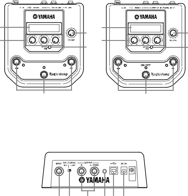
■ PANEL LAYOUT
• Top Panel
UB99A |
UB99B/UB99MK2 |
1 |
1 |
3 |
3 |
2 |
2 |
4 |
4 |
AUTO F.R. |
ON/OFF |
5 |
5 |
1Display
2CONTROL Knobs
3VOLUME Knob
4STORE/EXIT Button /
5[UB99A] – Switch, + Switch, AUTO F.R./ON/OFF Switch AUTO F.R./ON/OFF [UB99B/UB99MK2] – Switch, + Switch, ON/OFF Switch ON/OFF
•Rear Panel
PHONES
6 7 |
8 |
9 0 q |
6 INPUT Jack
7 INPUT LEVEL HIGH/LOW Switch
8OUTPUT L/MONO, R Jacks
9PHONES Jack
0 USB JackUSB
q AC IN Jack (Power Adaptor)
4

UB99MK2: |
UB99B: |
UB99A: |
SW101 |
|
|
IC102 (8P) |
|
+5A |
+3.3D |
IC105 (8P) |
|
|
|
|
|
|
||||
|
|
|
|
|
|
|
LPF |
|
|
|
|
|
|
|||||||
|
|
|
|
|
|
|
|
|
|
|
|
|
|
|
|
|
|
|
||
|
|
|
|
|
[Gain= +8dB] |
|
|
|
|
|
28 |
3 |
1 |
VR101 |
IC106 (8P) |
TR103 |
JK102 |
|||
00017-DIC |
00022-DIC |
00014-DIC |
3 1 |
|
2 |
- 1 |
6 - |
7 |
|
|
|
|
||||||||
|
2 |
|
|
27 |
2 |
TR101 |
|
3 |
1 |
|
,107 |
|
||||||||
IC101 (8P) |
|
|
|
|
3 IC104 |
|
|
|
|
|
|
|||||||||
|
|
|
|
|
5 |
7 |
|
|
|
|
|
|
||||||||
[Gain= -10dB] |
6 - |
7 |
|
(28P) |
26 |
|
IC106 |
|
|
|
||||||||||
JK101 |
+3.3D |
5 |
|
|
|
|
|
|
|
|||||||||||
|
|
|
|
2 |
- 1 |
4 |
25 |
|
TR102 |
|
5 |
7 |
|
|
|
|||||
|
|
|
|
|
|
|
|
|
|
|
|
6 |
|
|
|
|
||||
|
|
|
|
|
|
|
|
|
|
|
|
|
|
|
|
|
|
|
|
|
|
|
|
|
|
|
IC103 (8P) |
|
19 |
|
13,14 |
|
|
|
|
(8P) |
TR104 |
JK103 |
|||
|
|
|
IC3 (5P) |
SYSTEM |
|
|
|
|
|
|
|
|
|
|
|
|
|
|
,108 |
|
|
|
|
|
RESET |
|
|
|
|
|
|
|
|
|
|
|
3 |
1 |
|
|
|
|
|
|
|
4 |
|
|
|
|
|
|
|
|
|
|
|
|
|
|
||
|
|
|
|
|
|
|
|
|
|
|
|
|
|
|
|
|
IC114 (8P) |
|
||
|
|
|
|
|
|
|
|
|
X 1 |
|
|
|
|
|
|
5 |
7 |
PHONES |
||
|
|
|
+3.3D |
|
+3.3D |
|
|
|
|
|
|
|
|
|
|
|
||||
|
|
|
|
|
|
|
|
|
|
|
|
|
|
|
|
|
|
|||
|
|
|
IC1 (48P) |
IC2 (28P) |
|
|
+3.3D |
3 |
55,65 |
|
IC10 (44P) |
+3.3D |
|
|
|
|
|
JK105 |
||
|
|
|
|
|
|
|
|
|
|
|
IC5 |
|
|
|
|
|
|
|
||
|
|
|
|
|
|
|
|
|
|
|
|
|
|
|
|
|
|
|
|
|
|
|
|
12 |
|
|
|
|
|
|
(176P) |
|
|
|
|
|
|
|
|
||
|
|
|
X 2 |
|
|
|
|
|
15 |
|
|
|
|
+3.3D |
|
|
|
|
X 3 |
|
|
|
|
|
|
|
|
|
|
|
|
|
|
|
|
|
|
|
|
||
|
|
|
|
|
|
|
|
|
|
|
|
|
IC6 (44P) |
|
+3.3D |
|
|
+3.3D |
||
|
|
|
|
|
|
|
|
|
|
|
|
|
|
|
|
|
|
|
||
66,67
AN0 AN1 AN2 78 79 80
VR1 VR2 VR3
AN0 AN1 AN2
63 |
|
|
|
|
|
|
|
|
|
|
(AUTO F.R.) |
+ |
|
P6-0 |
P6-1 |
P6-2 |
- |
ON/OFF |
STORE/EXIT |
|
58 |
59 |
60 |
17 |
16 |
15 |
13 |
*1 |
LD1 |
LD2 |
LD3 |
*1 SW2 |
|
|
|
|
|
|
|
SW1 |
SW3 |
SW4 |
|
from P6_0 |
from P6_1 |
from P6_2 |
|
|
STORE/ EXIT |
|
|
|
|
|
|
|
|
|
|
|
TR1 |
TR2 |
TR3 |
|
|
|
|
*2 |
LD1 |
LD2 |
LD3 |
*2 |
|
|
|
|
|
|
|
SW2 |
|
|
|
|
|
|
|
SW1 |
SW3 |
SW4 |
|
from P6_0 |
from P6_1 |
from P6_2 |
|
|
|
|
|
|
|
TR2 |
TR3 |
|
|
STORE/ EXIT |
|
|
TR1 |
|
|
|
|
||
*1 indicates the name for the UB99A model. |
|
|
|
||||
*1 UB99A |
|
|
|
|
|||
*2 indicates the name for the UB99B/UB99MK2 models. |
DM |
||||||
*2 UB99B/UB99MK2 |
|
|
|
||||
|
12,13 |
IC4 (100P) |
IC7 (64P) |
 +5D
+5D
CN1 (16P)
TR105,106
A ZD103 ZD104
D106,107 |
IC113 |
D110,112 |
-15V |
|
|
A |
IC112 |
D109,111 |
+15V |
|
IC108 |
|
+5V |
|
IC109 |
D108 |
+5V |
|
IC111 |
|
+3.3V |
|
5
JK1
AC-10
AC IN
JK104
DIAGRAM BLOCK ■
UB99A/UB99B/UB99MK2
UB99A/UB99B/UB99MK2
■CIRCUIT BOARD LAYOUT
•Bottom view
DM
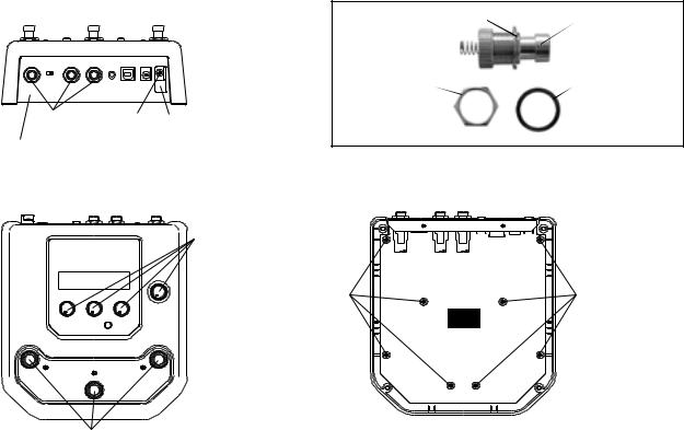
■ DISASSEMBLY PROCEDURES
1. |
Bottom Case |
1. |
( : 1 ) |
|
(Time required: about 1 minute) |
1-1. |
[40] 4 [30] 2 |
1-1. |
Remove the four (4) screws marked [40] and the two |
|
( 1) |
|
(2) screws marked [30]. The bottom case can then be |
|
|
|
removed. (Fig.1) |
|
|
• Bottom view
[30]
[40] |
[40] |
Bottom case
[30]: Bind Head Tapping Screw-B+ B 3.0X8 MFZN2BL (EP600190) [40]: Bind Head Tapping Screw-P+ P 4.0X8 MFZN2BL (VB931600)
Fig.1 1
6
2.Rear Panel (Time required: about 3 minutes)
2-1. Remove the bottom case. (See Procedure 1.) (Fig. 2) 2-2. Remove the screw marked [110], the three (3)
hexagonal nuts marked [120] and the three (3) flat washers marked [130] from the rear panel. AC cord column and the rear panel can then be removed. (Fig. 2)
3.DM Circuit Board
(Time required: about 3 minutes)
3-1. Remove the bottom case. (See Procedure 1.) 3-2. Remove the rear panel. (See Procedure 2.) 3-3. Remove the four (4) knobs from the front panel.
3-4. Remove the eight (8) screws marked [90]. The DM circuit board can then be removed. (Fig. 2)
4.Foot Switch (Time required: about 3 minutes)
4-1. Remove the bottom case. (See Procedure 1.) 4-2. Remove the rear panel. (See Procedure 2.)
4-3. Remove the DM circuit board. (See Procedure 3.) 4-4. Remove the hexagonal nut of the foot switch. The foot
switch can then be removed. (Fig.2, Photo. 1)
*Be sure to fit the projection of the foot switch panel to the groove of the foot swtich when attaching the foot switches.
UB99A/UB99B/UB99MK2
2.( : 3 )
2-1. (1 )
2-2. [110] 1 [120]3 [130] 3 AC( 2)
3.DM
( : 3 )
3-1. (1 ) 3-2. (2 )
3-3. 4 ( 2)
3-4. [90] 8 DM ( 2)
4.( : 3 )
4-1. (1 ) 4-2. (2 ) 4-3. DM (3 )
4-4. ( 2 1)
• |
Rear view |
|
|
|
|
|
|
Spring washer |
Foot switch |
|
|
|
|
|
|
|
|
Hexagonal nut |
Flat washer |
|
|
|
|
|
|
[120] |
[110] |
AC cord column |
|
|
[130] |
|
AC |
|
Rear panel |
Photo. 1 1 |
|
||
|
|
|
|
|
• |
Top view |
|
• Bottom view |
|
|
|
|
Knob |
|
|
|
|
[90] |
[90] |
|
|
|
DM |
|
Foot switch
Hexagonal nut
[90]: Bind Head Tapping Screw-P+ P 3.0X8 MFZN2BL (EP630220) [110]: Bind Head Screw+ 3.0X8 MFZN2BL (VA295800)
[120]: Hexagonal Nut 9.0 12X2 MFNI33 (LX200060) [130]: Flat Washer 9.0X14X0.5 MFNI33 (VL802300)
Fig.2 2
7

UB99A/UB99B/UB99MK2
■ LSI PIN DESCRIPTIONLSI
• HD6413008VF25 (X4196A00) CPU (MAIN) |
|
|
|
DM: IC4 |
||||
PIN |
NAME |
I/O |
FUNCTION |
PIN |
NAME |
I/O |
FUNCTION |
|
NO. |
|
|
|
NO. |
|
|
|
|
1 |
Vcc |
- |
Analog power supply +3.3V |
51 |
P26/A14 |
I/O |
|
|
2 |
_____ |
|
|
52 |
|
|
Port 2 / Address bus |
|
CS7/TMO0/TP8/PB0 |
I/O |
|
P27/A15 |
I/O |
||||
|
|
|||||||
3 |
_____ |
|
|
53 |
|
|
|
|
CS6/TMIO1/TP9/PB1 |
I/O |
Chip select / / / Port B |
P50/A16 |
I/O |
|
|||
4 |
_____ |
|
54 |
|
|
|
||
CS5/TMO2/TP10/PB2 |
I/O |
|
P51/A17 |
I/O |
Port 5 / Address bus |
|||
5 |
_____ |
|
|
55 |
|
|
||
CS4/TMIO3/TP11/PB3 |
I/O |
|
P52/A18 |
I/O |
|
|||
6 |
TP12/PB4 |
I/O |
|
56 |
P53/A19 |
I/O |
|
|
7 |
TP13/PB5 |
I/O |
Pulse output / Port B |
57 |
Vss |
- |
Ground |
|
8 |
|
|
58 |
_________ |
|
|
||
TP14/PB6 |
I/O |
|
P60/WAIT |
I/O |
|
|||
9 |
|
|
|
59 |
__________ |
|
Port 6 |
|
TP15/PB7 |
I/O |
|
P61/BREQ |
I/O |
||||
|
|
|||||||
10 |
__________ |
|
|
60 |
__________ |
|
|
|
RESO |
O |
Reset |
P62/BACK |
I/O |
|
|||
11 |
Vss |
- |
Ground |
61 |
P67/φ |
I/O |
Port 6 / System clock output |
|
12 |
|
|
|
62 |
_________ |
|
|
|
TXD0/P90 |
I/O |
|
STBY |
I |
Stand-by mode signal |
|||
13 |
|
|
Data transmission / Port 9 |
63 |
_______ |
|
|
|
TXD1/P91 |
I/O |
RES |
I |
Reset |
||||
|
||||||||
14 |
RXD0/P92 |
I/O |
Data reception / Port 9 |
64 |
NMI |
I |
Non-maskable interrupt |
|
15 |
RXD1/P93 |
I/O |
65 |
Vss |
- |
Ground |
||
|
||||||||
16 |
______ |
|
|
66 |
|
|
|
|
IRQ4/SCK0/P94 |
I/O |
|
EXTAL |
I |
Clock |
|||
17 |
______ |
|
Interrupt request / Serial clock / Port 9 |
67 |
|
|
|
|
IRQ5/SCK1/P95 |
I/O |
XTAL |
O |
Clock |
||||
|
||||||||
18 |
D0/P40 |
I/O |
|
68 |
Vcc |
- |
Power supply +3.3V |
|
19 |
|
|
|
69 |
_____ |
|
|
|
D1/P41 |
I/O |
Data bus / Port 4 |
P63/AS |
O |
|
|||
20 |
|
|
70 |
_____ |
|
|
||
D2/P42 |
I/O |
|
P64/RD |
O |
Port 6 |
|||
21 |
|
|
|
71 |
_________ |
|
||
D3/P43 |
I/O |
|
P65/HWR |
O |
|
|||
22 |
|
|
|
72 |
________ |
|
|
|
Vss |
- |
Ground |
P66/LWR |
O |
|
|||
23 |
D4/P44 |
I/O |
Data bus / Port 4 |
73 |
MD0 |
I |
Model control |
|
24 |
D5/P45 |
I/O |
74 |
MD1 |
I |
|||
|
|
|||||||
25 |
D6/P46 |
I/O |
|
75 |
MD2 |
I |
|
|
26 |
P47/D7 |
I/O |
Port 4 / Data bus |
76 |
AVcc |
- |
Power supply +3.3V for A/D |
|
27 |
P30/D8 |
I/O |
|
77 |
VREF |
I |
Reference voltage for A/D |
|
28 |
P31/D9 |
I/O |
|
78 |
AN0/P70 |
I |
|
|
29 |
P32/D10 |
I/O |
|
79 |
AN1/P71 |
I |
|
|
30 |
P33/D11 |
I/O |
Port 3 / Data bus |
80 |
AN2/P72 |
I |
Analog input / Port 7 |
|
31 |
P34/D12 |
I/O |
81 |
AN3/P73 |
I |
|||
|
||||||||
|
|
|||||||
32 |
P35/D13 |
I/O |
|
82 |
AN4/P74 |
I |
|
|
33 |
P36/D14 |
I/O |
|
83 |
AN5/P75 |
I |
|
|
34 |
P37/D15 |
I/O |
|
84 |
DA0/AN6/P76 |
I/O |
D/A output / Analog input / Port 7 |
|
35 |
Vcc |
- |
Analog power supply +3.3V |
85 |
DA1/AN7/P77 |
I/O |
||
|
||||||||
36 |
P10/A0 |
I/O |
|
86 |
AVss |
- |
Ground for A/D |
|
37 |
|
|
|
87 |
______ |
|
|
|
P11/A1 |
I/O |
|
IRQ0/P80 |
O |
Interrupt request / Port 8 |
|||
38 |
|
|
|
88 |
_____ ______ |
|
|
|
P12/A2 |
I/O |
|
CS3/IRQ1/P81 |
I/O |
|
|||
39 |
|
|
|
89 |
_____ ______ |
|
Chip select / Interrupt request / Port 8 |
|
P13/A3 |
I/O |
Port 1 / Address bus |
CS2/IRQ2/P82 |
I/O |
||||
|
||||||||
40 |
|
|
90 |
____________ _____ ______ |
|
|
||
P14/A4 |
I/O |
|
ADTRG/CS1/IRQ3/P83 |
I/O |
A/D trigger / Chip select / Interrupt request / Port 8 |
|||
41 |
|
|
|
91 |
_____ |
|
|
|
P15/A5 |
I/O |
|
CS0/P84 |
I/O |
Chip select / Port 8 |
|||
42 |
P16/A6 |
I/O |
|
92 |
Vss |
- |
Ground |
|
43 |
P17/A7 |
I/O |
|
93 |
TCLKA/TP0/PA0 |
I/O |
Timer clock / Pulse output / Port A |
|
44 |
Vss |
- |
Ground |
94 |
TCLKB/TP1/PA1 |
I/O |
||
|
||||||||
45 |
P20/A8 |
I/O |
|
95 |
TCLKC/TIOCA0/TP2/PA2 |
I/O |
Timer clock / Output comparison / Pulse output / Port A |
|
46 |
P21/A9 |
I/O |
|
96 |
TCLKD/TIOCB0/TP3/PA3 |
I/O |
Timer clock / Input capture / Pulse output / Port A |
|
47 |
P22/A10 |
I/O |
Port 2 / Address bus |
97 |
A23/TIOCA1/TP4/PA4 |
I/O |
Address bus / Output comparison / Pulse output / Port A |
|
48 |
P23/A11 |
I/O |
98 |
A22/TIOCB1/TP5/PA5 |
I/O |
Address bus / Input capture / Pulse output / Port A |
||
|
||||||||
49 |
P24/A12 |
I/O |
|
99 |
A21/TIOCA2/TP6/PA6 |
I/O |
Address bus / Output comparison / Pulse output / Port A |
|
50 |
P25/A13 |
I/O |
|
100 |
A20/TIOCB2/TP7/PA7 |
I/O |
Address bus / Input capture / Pulse output / Port A |
|
8
• M38K07M4L-303HP (X3921200) CPU (USB)
UB99A/UB99B/UB99MK2
DM: IC7
PIN |
NAME |
I/O |
FUNCTION |
PIN |
NAME |
I/O |
FUNCTION |
|
NO. |
|
|
|
NO. |
|
|
|
|
1 |
P12/DQ2/AN2 |
I/O |
|
33 |
P26 |
I/O |
Port P2 (In/output) |
|
2 |
P13/DQ3/AN3 |
I/O |
|
34 |
P27 |
I/O |
||
|
|
|||||||
3 |
P14/DQ4/AN4 |
I/O |
Port P1 (In/output) |
35 |
P50/INT0 |
I/O |
Port P5 (In/output)/Interruption input |
|
4 |
P15/DQ5/AN5 |
I/O |
36 |
P51/CNTR0 |
I/O |
Port P5 (In/output)/Timer X function |
||
|
||||||||
5 |
P16/DQ6/AN6 |
I/O |
|
37 |
P52/INT1 |
I/O |
Port P5 (In/output)/Interruption input |
|
6 |
P17/DQ7/AN7 |
I/O |
|
38 |
P53 |
I/O |
|
|
7 |
CNVSS |
- |
Ground |
39 |
P54 |
I/O |
|
|
8 |
____________ |
|
|
40 |
|
|
Port P5 (In/output) |
|
RESET |
I |
System reset input |
P55 |
I/O |
||||
9 |
EccE |
- |
Analog power supply +3.3V |
41 |
P56 |
I/O |
|
|
10 |
VREF |
I |
Reference voltage input |
42 |
P57 |
I/O |
|
|
11 |
Vss |
- |
Ground |
43 |
P00 |
I/O |
|
|
12 |
XIN |
I |
Clock input |
44 |
P01 |
I/O |
|
|
13 |
XOUT |
O |
Clock output |
45 |
P02 |
I/O |
|
|
14 |
Vcc |
- |
Power supply +3.3V |
46 |
P03 |
I/O |
Port P0 (In/output) |
|
15 |
CNVSS2 |
- |
Ground |
47 |
P04 |
I/O |
||
|
||||||||
16 |
P60(LED0) |
I/O |
|
48 |
P05 |
I/O |
|
|
17 |
P61(LED1) |
I/O |
Port P6 (In/output) |
49 |
P06 |
I/O |
|
|
18 |
P62(LED2) |
I/O |
50 |
P07 |
I/O |
|
||
|
|
|||||||
19 |
P63(LED3) |
I/O |
|
51 |
P40/EXDREQ/RXD |
I/O |
|
|
20 |
PVss |
- |
|
52 |
P41/EXDACK/TXD |
I/O |
Port P4 (In/output)/External bus interface/Serial I/O |
|
21 |
|
|
Analog power supply +3.3V |
53 |
_______ |
|
||
PVcc |
- |
P42/EXTC/SCLK |
I/O |
|
||||
|
|
|||||||
22 |
DVcc |
- |
|
54 |
P43/EXA1/SRDY |
I/O |
|
|
23 |
USBVREF |
- |
USB reference power supply |
55 |
P30 |
I/O |
Port P3 (In/output) |
|
24 |
TrON |
O |
USB reference volyage output |
56 |
P31 |
I/O |
||
|
||||||||
25 |
D0+ |
I/O |
USB upstream in/output |
57 |
P32 |
I/O |
|
|
26 |
D0- |
I/O |
58 |
P33/EXINT |
I/O |
|
||
|
|
|||||||
27 |
P20 |
I/O |
|
59 |
P34/EXCS |
I/O |
|
|
28 |
P21 |
I/O |
|
60 |
P35/EXWR |
I/O |
Port P3 (In/output)/External bus interface |
|
29 |
P22 |
I/O |
Port P2 (In/output) |
61 |
P36/EXRD |
I/O |
|
|
30 |
P23 |
I/O |
62 |
P37/EXA0 |
I/O |
|
||
|
|
|||||||
31 |
P24 |
I/O |
|
63 |
P10/DQ0/AN0 |
I/O |
Port P1 (In/output) |
|
32 |
P25 |
I/O |
|
64 |
P11/DQ1/AN1 |
I/O |
||
|
|
• AK4528VF (XY624A00) ADC/DAC (CMOS A/D & D/A Converter) |
DM: IC104 |
|||||||
PIN |
NAME |
I/O |
FUNCTION |
PIN |
NAME |
I/O |
FUNCTION |
|
NO. |
|
|
|
NO. |
|
|
|
|
1 |
VCOM |
O |
Common voltage output , VA/2 |
15 |
CKS0 |
I |
Master clock select |
|
2 |
AINR+ |
I |
Rch analog positive input |
16 |
CKS1 |
I |
|
|
|
|
|||||||
3 |
AINR- |
I |
Rch analog negative input |
17 |
DIF |
I |
Digital audio interface select |
|
4 |
AINL+ |
I |
Lch analog positive input |
18 |
DFS |
I |
Double speed sampling mode |
|
5 |
AINL- |
I |
Lch analog negative input |
19 |
PDN |
I |
Power-down mode |
|
6 |
VREF |
I |
Reference voltage |
20 |
DEM0 |
I |
De-emphasis frequency select |
|
7 |
AGND |
- |
Analog ground +3.3V |
21 |
DEM1 |
I |
|
|
|
|
|||||||
8 |
VA |
- |
Analog power supply |
22 |
VT |
- |
Output buffer power supply |
|
9 |
P/S |
I |
Paralle/serial mode select |
23 |
VD |
- |
Digital power supply |
|
10 |
MCLK |
I |
Master clock input |
24 |
DGND |
- |
Digital ground |
|
11 |
LRCK |
I |
Input/output channel clock |
25 |
AOUTL- |
O |
Lch analog negative output |
|
12 |
BICK |
I |
Audio serial data clock |
26 |
AOUTL+ |
O |
Lch analog positive output |
|
13 |
SDTO |
O |
Audio serial data output |
27 |
AOUTR- |
O |
Rch analog negative output |
|
14 |
SDTI |
I |
Audio serial data input |
28 |
AOUTR+ |
O |
Rch analog positive output |
|
9
UB99A/UB99B/UB99MK2
• YSS910-V (XV988B00) DSP6 (Digital Signal Processor) |
|
DM: IC5 |
||||||
PIN |
NAME |
I/O |
FUNCTION |
PIN |
NAME |
I/O |
FUNCTION |
|
NO. |
NO. |
|||||||
|
|
|
|
|
|
|||
1 |
Vdd |
- |
Power supply (3.3 V) |
89 |
Vss |
- |
Ground |
|
2 |
Vss |
- |
Ground |
90 |
DB13 |
I/O |
|
|
3 |
XI |
I |
System master clock input (60 MHz or 30 MHz) |
91 |
DB14 |
I/O |
|
|
4 |
XO |
O |
System master clock output (High or 30 MHz) |
92 |
DB15 |
I/O |
|
|
5 |
Vdd5 |
- |
Power supply (5 V) |
93 |
DB16 |
I/O |
|
|
6 |
/SYNCI |
I |
System sync. signal input |
94 |
DB17 |
I/O |
Parallel data bus |
|
7 |
/SYNCO |
O |
System sync. signal output |
95 |
DB18 |
I/O |
||
|
||||||||
8 |
Vdd5 |
- |
Power supply (5 V) |
96 |
DB19 |
I/O |
|
|
9 |
CKI |
I |
System clock input (30 MHz) |
97 |
DB20 |
I/O |
|
|
10 |
CKO |
O |
System clock output (30 MHz) |
98 |
DB21 |
I/O |
|
|
11 |
CKSEL |
I |
System master clock select (0: 60 MHz, 1: 30 MHz) |
99 |
DB22 |
I/O |
|
|
12 |
Vss |
- |
Ground |
100 |
Vss |
- |
Ground |
|
13 |
MCKS |
I |
Serial I/O master clock input (128 x Fs) |
101 |
Vdd |
- |
Power supply (3.3 V) |
|
14 |
/SSYNC |
I |
Serial I/O Sync. signal output |
102 |
DB23 |
I/O |
|
|
15 |
/IC |
I |
Initial clear (RESET) |
103 |
DB24 |
I/O |
|
|
16 |
/TEST |
I |
Test mode setting (0: Test, 1: Normal) |
104 |
DB25 |
I/O |
|
|
17 |
BTYP |
I |
Data bus type select (0: 8 bit, 1: 16 bit) |
105 |
DB26 |
I/O |
Parallel data bus |
|
18 |
/IRQ |
O |
IRQ output |
106 |
DB27 |
I/O |
||
19 |
TRIG |
I/O |
Trigger signal input/output |
107 |
DB28 |
I/O |
|
|
20 |
Vdd5 |
- |
Power supply (5 V) |
108 |
DB29 |
I/O |
|
|
21 |
Vss |
- |
Ground |
109 |
DB30 |
I/O |
|
|
22 |
/CS |
I |
Chip select signal input |
110 |
DB31 |
I/O |
|
|
23 |
/WR |
I |
Write signal input |
111 |
TIMO/DBOB |
I/O |
Timing signal output/ Parallel data bus output control input |
|
24 |
/RD |
I |
Read signal input |
112 |
Vss |
- |
Ground |
|
25 |
CA7 |
I |
|
113 |
Vdd5 |
- |
Power supply (5 V) |
|
26 |
CA6 |
I |
|
114 |
DA00 |
I/O |
|
|
27 |
CA5 |
I |
Address bus of internal register |
115 |
DA01 |
I/O |
|
|
28 |
CA4 |
I |
116 |
DA02 |
I/O |
|
||
29 |
CA3 |
I |
|
117 |
DA03 |
I/O |
Memory data bus |
|
30 |
CA2 |
I |
|
118 |
DA04 |
I/O |
||
31 |
CA1 |
I |
|
119 |
DA05 |
I/O |
|
|
32 |
Vss |
- |
Ground |
120 |
DA06 |
I/O |
|
|
33 |
Vdd |
- |
Power supply (3.3 V) |
121 |
DA07 |
I/O |
|
|
34 |
CD15 |
I/O |
|
122 |
Vss |
- |
Ground |
|
35 |
CD14 |
I/O |
|
123 |
DA08 |
I/O |
|
|
36 |
CD13 |
I/O |
|
124 |
DA09 |
I/O |
|
|
37 |
CD12 |
I/O |
Data bus of internal register |
125 |
DA10 |
I/O |
|
|
38 |
CD11 |
I/O |
126 |
DA11 |
I/O |
Memory data bus |
||
|
||||||||
39 |
CD10 |
I/O |
|
127 |
DA12 |
I/O |
||
40 |
CD09 |
I/O |
|
128 |
DA13 |
I/O |
|
|
41 |
CD08 |
I/O |
|
129 |
DA14 |
I/O |
|
|
42 |
CD07 |
I/O |
|
130 |
DA15 |
I/O |
|
|
43 |
CD06 |
I/O |
|
131 |
Vss |
- |
Ground |
|
44 |
Vss |
- |
Ground |
132 |
Vdd |
- |
Power supply (3.3 V) |
|
45 |
Vdd |
- |
Power supply (3.3 V) |
133 |
(n.c) |
- |
Not used |
|
46 |
Vdd5 |
- |
Power supply (5 V) |
134 |
Vdd5 |
- |
Power supply (5 V) |
|
47 |
CD05 |
I/O |
|
135 |
DA16 |
I/O |
|
|
48 |
CD04 |
I/O |
Data bus of internal register |
136 |
DA17 |
I/O |
|
|
49 |
CD03 |
I/O |
137 |
DA18 |
I/O |
|
||
50 |
CD02 |
I/O |
|
138 |
DA19 |
I/O |
Memory data bus |
|
51 |
CD01 |
I/O |
|
139 |
DA20 |
I/O |
||
52 |
CD00 |
I/O |
|
140 |
DA21 |
I/O |
|
|
53 |
/WAIT |
O |
WAIT output |
141 |
DA22 |
I/O |
|
|
54 |
Vss |
- |
Ground |
142 |
DA23 |
I/O |
|
|
55 |
SI0 |
I |
|
143 |
Vss |
- |
Ground |
|
56 |
SI1 |
I |
|
144 |
DA24 |
I/O |
|
|
57 |
SI2 |
I |
Serial data input |
145 |
DA25 |
I/O |
|
|
58 |
SI3 |
I |
146 |
DA26 |
I/O |
|
||
59 |
SI4 |
I |
|
147 |
DA27 |
I/O |
Memory data bus |
|
60 |
SI5 |
I |
|
148 |
DA28 |
I/O |
||
61 |
SI6 |
I |
|
149 |
DA29 |
I/O |
|
|
62 |
SI7 |
I |
|
150 |
DA30 |
I/O |
|
|
63 |
Vss |
- |
Ground |
151 |
DA31 |
I/O |
|
|
64 |
Vdd5 |
- |
Power supply (5 V) |
152 |
Vdd5 |
- |
Power supply (5 V) |
|
65 |
SO0 |
O |
|
153 |
Vss |
- |
Ground |
|
66 |
SO1 |
O |
|
154 |
A00 |
O |
|
|
67 |
SO2 |
O |
Serial data output |
155 |
A01 |
O |
|
|
68 |
SO3 |
O |
156 |
A02 |
O |
|
||
69 |
SO4 |
O |
|
157 |
A03 |
O |
|
|
70 |
SO5 |
O |
|
158 |
A04 |
O |
Memory address (SRAM, PSRAM, DRAM) |
|
71 |
SO6 |
O |
|
159 |
A05 |
O |
||
|
|
|||||||
72 |
SO7 |
O |
|
160 |
A06 |
O |
|
|
73 |
Vss |
- |
Ground |
161 |
A07 |
O |
|
|
74 |
DB00 |
I/O |
|
162 |
A08 |
O |
|
|
75 |
DB01 |
I/O |
|
163 |
A09 |
O |
|
|
76 |
DB02 |
I/O |
|
164 |
Vss |
- |
Ground |
|
77 |
DB03 |
I/O |
|
165 |
Vdd |
- |
Power supply (3.3 V) |
|
78 |
DB04 |
I/O |
|
166 |
A10 |
O |
Memory address (SRAM, PSRAM, DRAM) |
|
79 |
DB05 |
I/O |
Parallel data bus |
167 |
A11 |
O |
||
|
||||||||
80 |
DB06 |
I/O |
168 |
A12 |
O |
|
||
|
Memory address (SRAM, PSRAM) |
|||||||
81 |
DB07 |
I/O |
|
169 |
A13 |
O |
||
82 |
DB08 |
I/O |
|
170 |
A14 |
O |
|
|
83 |
DB09 |
I/O |
|
171 |
A15/RAS |
O |
Memory address (SRAM, PSRAM), /RAS (DRAM) |
|
84 |
DB10 |
I/O |
|
172 |
A16/CAS |
O |
Memory address (SRAM, PSRAM), /CAS (DRAM) |
|
85 |
DB11 |
I/O |
|
173 |
A17/CE |
O |
Memory address (SRAM), /CE (PSRAM) |
|
86 |
DB12 |
I/O |
|
174 |
/WE |
O |
Memory write enable signal |
|
87 |
Vdd5 |
- |
Power supply (5 V) |
175 |
/OE |
O |
Memory output enable signal |
|
88 |
Vdd |
- |
Power supply (3.3 V) |
176 |
Vdd5 |
- |
Power supply (5 V) |
|
10
 Loading...