


SLV-E850UX
Sony SLV-E850UX, SLV-F900NP, SLV-E880EG, SLV-F900B, SLV-F900UX Service Manual
...
SLV-E850B/E850UX/E880EG/F900B/F900NP/F900UX/
F900VC/F990B/F990NP/F990UX/F990VC
RMT-V222C/V222D/V222E/V223C/V240/V240A/V240B/V240C/V240D
French Model
SLV -E850B/F900B/F990B
UK Model
SLV-E850UX/F900UX/F990UX
Greek Model
SLV-E880EG
Spanish Model
SLV-F900NP/F990NP
Germany Model
SLV-F900VC/F990VC
SERVICE MANUAL
VIDEO CASSETTE RECORDER
MICROFILM
S MECHANISM
• Refer to the SERVICE MANUAL of VHS MECHANICAL
ADJUSTMENTS for MECHANICAL ADJUSTMENTS.
(9-921-647-11)
G
j
SPECIFICATIONS
Photo : SLV-F990
SLV-E850B/E850UX/E880EG/F900B/F900NP/F900UX/F900VC/F990B/F990NP/F990UX/F990VC
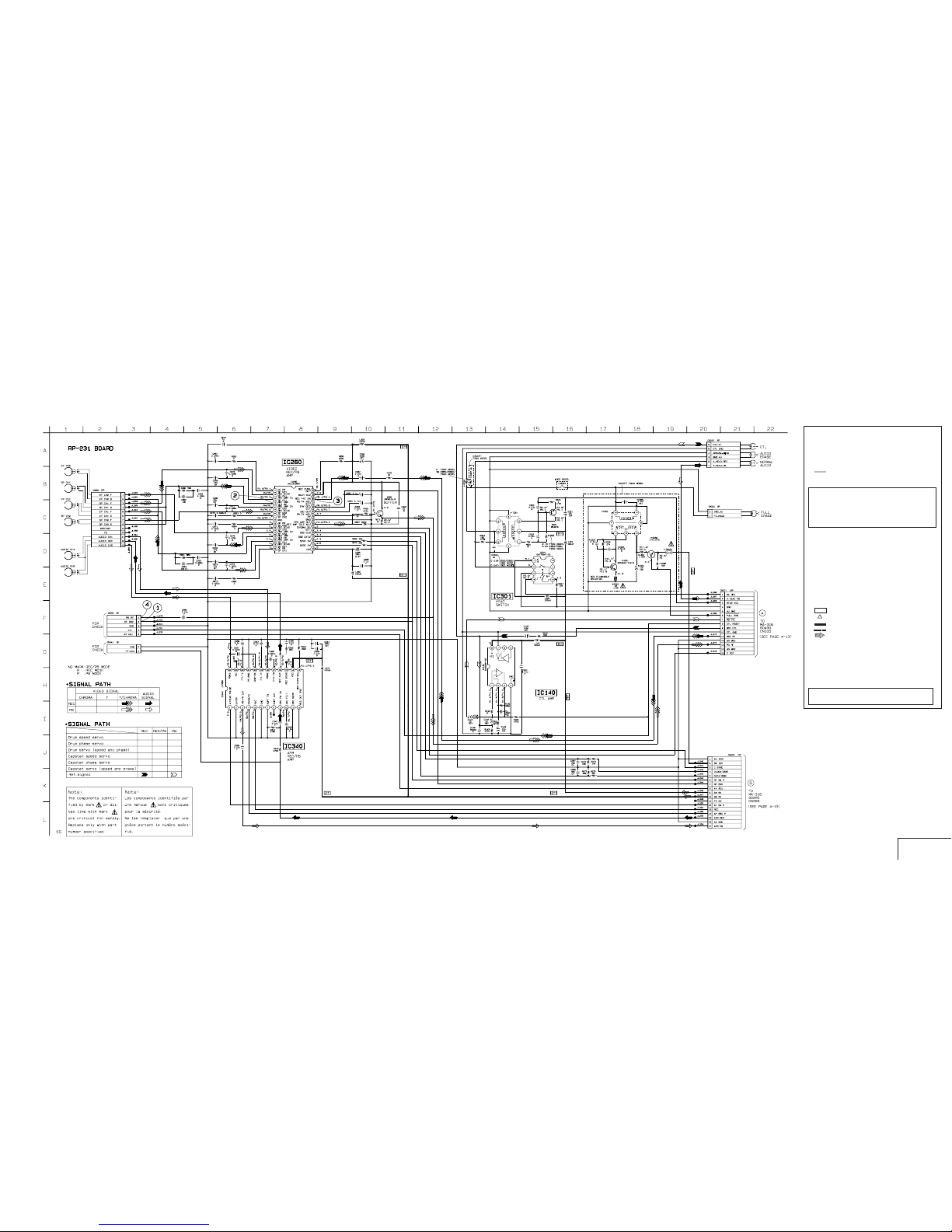
RP-231 (REC/PB AMP) SCHEMATIC DIAGRAM
— Ref. No.: RP-231 Board; 1,000 Series —
• For printed wiring boards.
• : Pattern from the side which enables seeing.
•
+
: Through hole.
Caution :
Pattern face side: Parts on the pattern face side
(Conductor Side) seen from the pattern face are
indicated.
Pattern face side: parts on the parts face side seen
(Component Side) from the parts face are indicated.
• For schematic diagrams.
• Caution when replacing chip parts.
New parts must be attached after removal of chip.
Be careful not to heat the minus side of tantalum
capacitor, because it is damaged by the heat.
• All resistor are in ohms, 1/4W unless otherwise noted.
Chip resistor are 1/10W unless otherwise noted.
kΩ: 1000Ω, MΩ, : 1000kΩ.
• All capacitors are in µF unless otherwise noted. pF : µ
µF. 50V or less are not indicated except for electrolytics
and tantalums.
• : panel designation.
• : internal component.
• : B+ Line.
•
: B– Line.
• : IN/OUT direction of (+,–) B LINE.
• Circled numbers refer to waveforms.
• Readings are taken with a PAL color-bar signal input.
• Voltage are dc between ground and measurement points.
• Readings are taken with a digital multimeter (DC10MΩ).
• Voltage variations may be noted due to normal production
tolerances.
When indicating parts by reference number, please
include the board name.
THIS NOTE IS COMMON FOR PRINTED WIRING
BOARDS AND SCHEMATIC DIAGRAMS.
(In addition to this, the necessary note is
printed in each block.)
4-5 4-6 4-7
REC/PB AMP
RP-231
SLV-E850B/E850UX/E880EG/F900B/F900NP/F900UX/F900VC/F990B/F990NP/F990UX/F990VC
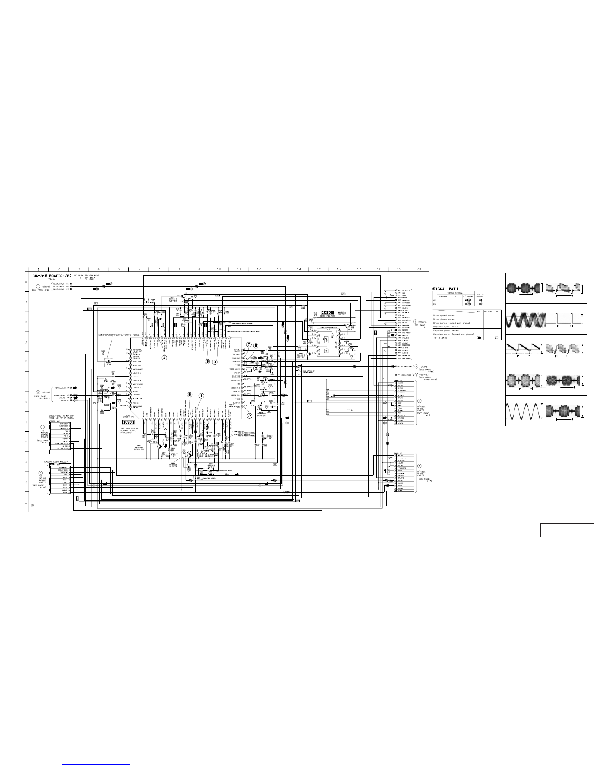
MA-316 (VIDEO, NORMAL AUDIO) SCHEMATIC DIAGRAM
— Ref. No.: MA-316 Board; 2,000 Series —
4-11 4-12 4-13
VIDEO, NORMAL AUDIO
MA-316 (1/8)
MA-316
BOARD
(1/3)
1
IC201 !∞ REC
1
IC201 !∞ PB
2
IC201 @∞ REC
0.1µsec/div
0.2V/div
5
IC201 #∞ REC
6
IC201 #¶ REC/PB
4.2Vp-p
H
7
IC201 #• REC
440mVp-p
H
3
IC201 $• REC
0.34Vp-p
H
4
IC201 ^º REC/PB
0.6Vp-p
1Vp-p
H
8
IC201 !¢ REC
9
IC201 $∞ PB
470mVp-p
H
75mVp-p
H
4.43MHz
2.4Vp-p
H
0.42Vp-p
H

SLV-E850B/E850UX/E880EG/F900B/F900NP/F900UX/F900VC/F990B/F990NP/F990UX/F990VC
• See page 4-9 for MA-316 BOARD printed wiring board.MA-316 (SERVO/SYSTEM CONTROL) SCHEMATIC DIAGRAM
— Ref. No.: MA-316 Board; 2,000 Series —
4-14 4-15 4-16
SERVO/SYSTEM CONTROL
MA-316 (2/8)
MA-316
BOARD
(2/3)
!™
CN101 3 REC/PB
!£
CN101 4 REC/PB
!¢
CN102 3, IC160 &º
REC/PB
5Vp-p
758Hz
!∞
IC160 7 REC/PB
4Vp-p
25Hz
!§
IC160 $™ REC/PB
4Vp-p
5Vp-p
25Hz
16MHz
!¶
IC160 1, REC/PB
!•
IC160 ^¶ REC/PB
5Vp-p
300Hz
100
5Vp-p
25Hz
5Vp-p
25Hz
SLV-E850B/E850UX/E880EG/F900B/F900NP/F900UX/F900VC/F990B/F990NP/F990UX/F990VC
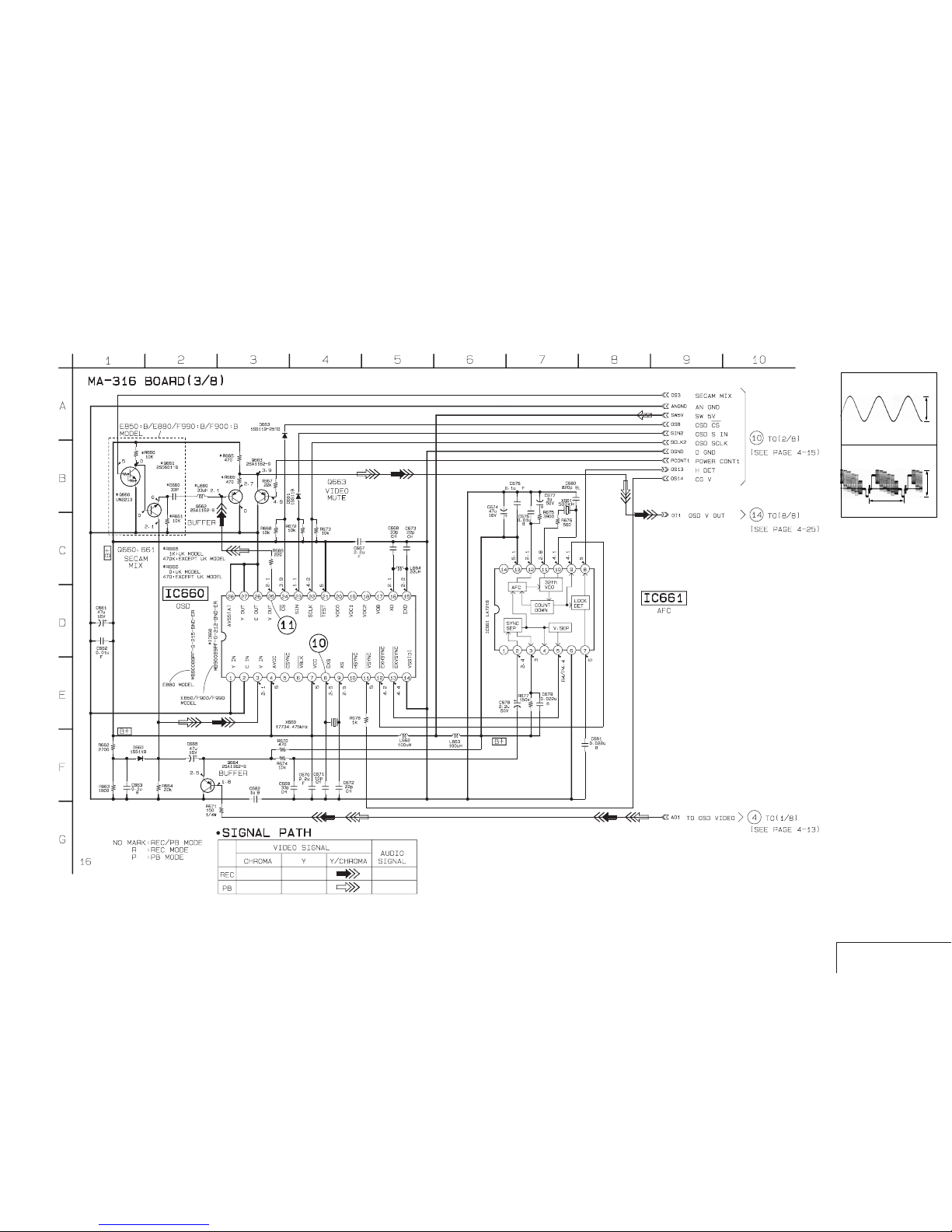
MA-316 (ON SCREEN DISPLAY) SCHEMATIC DIAGRAM
— Ref. No.: MA-316 Board; 2,000 Series —
• See page 4-9 for MA-316 BOARD printed wiring board.
4-17 4-18
ON SCREEN DISPLAY
MA-316 (3/8)
MA-316
BOARD
(3/3)
!º
IC660 8 REC/PB
!¡
IC660 @∞ REC/PB
17.73MHz
5.5Vp-p
2.4Vp-p
H
SLV-E850B/E850UX/E880EG/F900B/F900NP/F900UX/F900VC/F990B/F990NP/F990UX/F990VC
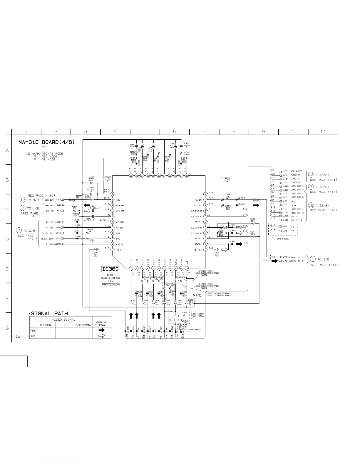
MA-316 (AFM AUDIO) SCHEMATIC DIAGRAM
— Ref. No.: MA-316 Board; 2,000 Series —
• See page 4-9 for MA-316 BOARD printed wiring board.
4-19 4-20
AFM AUDIO
MA-316 (4/8)
 Loading...