


LH5481D-25
Sharp LH5481D-25, LH5481D-15, LH5491U-35, LH5491U-15, LH5491D-35 Datasheet
...
LH5481
LH5491
FEATURES
•• Fastes t 64 × 8/9 Cascadable FIFO
35/25/15 MHz
•• Expandable in Word Width and
FIFO Depth
•• Almost- Full/ Almost -Em pty a nd
Half-Full Flags
•• Fully Ind ependent Asynchro nous
Inputs and Output s
•• LH5481 Output Enable forces Data
Output s to High-Impedance State
•• Pin-Compatible Replacements for Cypress
CY7C408A/09A or L ogic Devices
L8C408/09 FIFOs
•• Industry Standard Pinout
•• Packages:
28-Pin, 300-mil DIP
28-Pin PLCC
FUNCTIONAL DESCRIPTION
The LH5481 and LH5491 are high-performance , asyn-
chronous First-In, First-O ut (FIFO) memories organized
64 words deep b y eight or nine bits wide. The eight-bit
LH5481 has an Out put Enable ( OE) function, which can
be used to force the eig ht data out puts (DO) to a high -impedance stat e. The LH5491 has nine da ta outp uts.
These FI FOs acc ept eight or nine- bit dat a at the Data
Inputs (DI). A Shift In (SI) signal writes the DI data into the
FIFO. A Shif t Out (SO) sign al shift s stor ed data to the Data
Outputs (DO). The Ou tput Ready (OR) signal i ndicates
when valid data is present on the DO outputs.
If the FIFO is full and unable to accep t more DI data ,
Input Ready (IR) will not return HIG H, and SI pulses will
be ignored. If the FIFO is empty and unab le to shift data
to the DO outputs, OR will not return HIGH, and SO
pulses will be ignored. The Almost-Full/Almost-Empty
(AFE) flag is asserted (HIGH) when the FIFO is almost-full
(56 wor ds or more) or alm ost- em pty (eight words or les s).
The Half-Fu ll (HF) flag is ass erted ( HIGH) when the FI FO
contains 32 words or more .
Reading and writing operat ions may be asynchr onous,
allowing these FIFOs to be used as buffers between
digital machines of different oper ating frequencies. The
high speed make s these FIFOs ideal for high performance communication and contr oller applications.
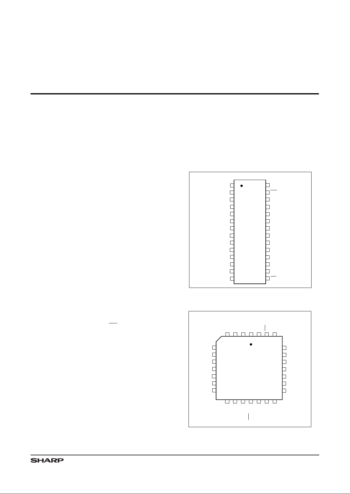
PIN CONNECTIONS
5481-1D
1
2
3
4
5
6
7
8
9
10
11
12
13
14
AFE
HF
IR
SI
DI
0
DI
1
V
SS
DI
2
DI
3
DI
4
DI
5
DI
6
DI
7
NC/DI
8
28
27
26
25
24
23
22
21
20
19
18
17
16
15
V
CC
MR
SO
OR
DO
0
DO
1
V
SS
DO
2
DO
3
DO
4
DO
5
DO
6
DO
7
OE/DO
8
28-PIN PDIP TOP VIEW
Figure 1. Pin Connections for DIP Package
5481-2D
1
2
3
4
5
6
7
8
9
10
11
12
13
14
DI
0
DI
1
DI
2
DI
3
DI
4
DI
5
28
27
26
25
24
23
22
21
20
19
18
17
16
15
OR
DO
0
DO
1
DO
2
DO
3
DO
4
SI
IR
HF
AFE
V
CC
MR
SO
DI6DI
7
NC/DI
8
OE/DO
8
DO
7
DO
6
DO
5
28-PIN PLCC
TOP VIEW
V
SS
V
SS
Figure 2. Pin Connections for PLCC Package
Cascadable 64 × 8 FIFO
Cascadable 64 × 9 FIFO
1
PIN DESCRIPTIONS
PIN PIN TYPE * DESCRIPTION
DI0 – DI
7 I
Data Input s, LH5481
DO0 – DO
7
O/Z
Data O u t pu t s, LH5481
DI0 – DI
8
I
Data Input s, LH5491
DO0 – DO
8
O
Data O u t pu t s, LH5491
SI
I
Shift In
SO
I
Shift Out
IR
O
Input Ready
OR
O
Output Ready
* I = Input, O = Output, Z = High-Impedance, V = Power Voltage Level
PIN PIN TYPE * DESCRIPTION
HF
O
Half-Full Flag
AFE
O
Alm ost -Fu ll / Almost -
Empt y
MR
I
Master Reset
OE
I
Output Enable
(LH5481 only)
V
CC
V
Positive Power Supply
V
SS
V
Ground
5481-3
WRITE POINTER
WRITE MULTIPLEXER
MEMORY ARRAY
READ MULTIPLEXER
READ POINTER
INPUT
CONTROL
LOGIC
DATA IN
MASTER
RESET
SI
IR
(LH5491) DI0 - DI
8
(LH5481) DI0 - DI
7
MR
ALMOST-FULL/
ALMOST-EMPTY
HALF-FULL
DATA OUT
OUTPUT
CONTROL
LOGIC
AFE
HF
DO
0
DO
7
OR
SO
DO
8
(LH5491)
OE
(LH5481)
.
.
.
.
.
.
Figure 3. LH5481/ 91 Bl o ck Diagr am
LH5481/91 64 × 8 / 64 × 9 FIFO
2

ABSOL UTE MAXI MUM RATING S
1,2
PARAMETER RATING
Vcc Range –0.5 V to 7 V
Input Vo ltage Range –0.5 V to Vcc + 0.5 V (not to exceed 7 V)
DC Out put Current
3
±40 mA
Storag e Temper at ur e –65oC to 150oC
DC Voltage Appl ied T o Output s In High-Z state –0.5 V to Vcc + 0.5 V (not to exceed 7 V)
Sta tic Discharge Vol tage
4
> 2000 V
Power Dissipation (Packag e Limit) 1.0 W
NOTES:
1. All voltages are measured with respect to Vss.
2. Stresses greater than those listed under ‘Absolute Maximum Ratings’ may cause permanent damage to the dev ice.
This is a stress rating for transient conditions only. Functional operation of the device at these or any other conditions
above those indicated in the ‘Operating Range’ o f this specification is not implied. Exposure to abs olute maximum r at ing
conditions for extended periods may affect device reliability.
3. Outputs should not be shorted for more than 30 seconds. No more than one output should be short ed at any time.
4. Sample tested onl y.
OPERATING RANGE
1
PARAMETER DESCRIPTION MIN MAX UNIT
T
A
Temp eratu re, Amb ient
0.0 70
o
C
V
CC
Supply Vol tage
4.5 5.5 V
Vss Ground
0.0 0.0 V
V
IL
Input Low Voltag e (Lo g ic ‘0’)
2
–0.5 0.8 V
V
IH
Input High Volta ge (Logic ‘1’)
2.0 Vcc + 0.5 V
NOTES:
1. All voltages are measured with respect to Vss.
2. FIFO inputs are able to withstand a –1.5 V undershoot for less than 10 ns per cycle.
DC ELECTRICAL CHARACTERIS TIC S 1 (Over Operating Range Unless Otherwise Noted)
PARAMETER DESCRI PTION TEST CONDITIONS MIN MAX UNIT
I
LI
Input Leakage Current VCC = 5. 5 V, VIN = 0 V to V
CC
–10 10
µA
I
LO
Output Leakage Current (High-Z ) VCC = 5. 5 V, V
OUT
= 0 V to V
CC
–10 10 µA
V
OH
Output High Voltage VCC = 4. 5 V, IOH = –4 mA
2.4 V
V
OL
Output Low Voltage VCC = 4. 5 V, IOL = 8.0 mA
0.4 V
I
CCQ
Power Supply Quiescent Current
VCC = 5. 5 V, I
OUT
= 0 mA
V
IN
≤ V
IL, VIN ≥ VIH
25 mA
I
CC
Power Supply Curr ent
2
fsi = 35 MHz, fso = 35 MHz
45 mA
NOTES:
1. All voltages are measured with respect to Vss.
2. Icc is dependent upon actual output loading and cycle rates. Specified values are with outputs open.
64 × 8 / 64 × 9 FIFO LH5481/91
3
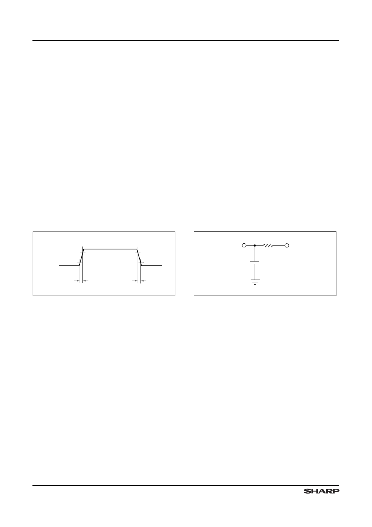
AC TEST CONDIT IO NS
1
PARAMETER RATING
Input Pulse Levels
0 to 3 V
Input Rise a nd Fall Tim es (10% / 90%)
Figure 4a
Input Timing Ref er ence Le vels
1.5 V
Output T iming Ref ere nce Lev e ls
1.5 V
Output Load for AC Timing Tests
Figure 4b
NOTE:
1. All vol tages are measured with respect to Vss.
CAPACITANCE
1,2
PARAMETER DESCRIPTION TEST CONDITIONS RATING
C
IN
Input Capacitanc e
TA = 2 5 °C, f = 1 MHz, VCC = 4.5 V 5 pF
C
OUT
Output Ca pacit ance TA = 2 5oC, f = 1 MHz, Vcc = 4.5 V
7 pF
NOTES:
1. All vol tages are measured with respect to Vss.
2. Sample tested onl y.
167 Ω
1.73 V
DEVICE
UNDER
TEST
CL = 30 pF *
5481-4
* INCLUDES JIG AND SCOPE CAPACITANCES
Figu r e 4b. Output Load Circuit
GND
10%10%
90%
90%
5 ns
5 ns
5481-18
3.0 V
Figur e 4a. Input Rise and Fall Ti mes
LH5481/91 64 × 8 / 64 × 9 FIFO
4

AC ELECTRI CAL CHARACTERIS TICS 1 (Over Operating Range)
SYMBOL PARAMETER
15MHz 25MHz 35MHz
UNITS
MIN MAX MIN MAX MIN MAX
f
O
Operating Frequency
2
15 25 35 MHz
t
PHSI
SI HIGH Time
3,8
15 11 9 ns
t
PLSI
SI LOW Time
3,8
20 18 17 ns
t
SSI
Data Setup to SI
4
–1 –1 –1 ns
t
HSI
Data Hold from SI
4
14 12 10 ns
t
DLIR
Delay, SI HIGH to IR LOW 20 18 16 ns
t
DHIR
Delay, SI LOW to IR HIGH 24 20 18 ns
t
PHSO
SO HIGH Time
3
15 11 9 ns
t
PLSO
SO LOW Time
3
20 18 17 ns
t
DLOR
Delay, SO HIGH to OR LOW 20 18 16 ns
t
DHOR
Delay, SO LOW to OR HIGH 24 20 18 ns
t
SOR
Data Setup to OR HIGH –1 –1 –1 ns
t
HSO
Data Hold from SO LOW 0 0 0 ns
t
FT
Fallt hrou gh T im e 36 34 30 ns
t
BT
Bubblethrough Time 28 26 25 ns
t
SIR
Data Setup to IR
5
555ns
t
HIR
Data Hold from IR
5
555ns
t
PIR
Input Ready Pulse HIGH
8
777ns
t
POR
Output Ready Pulse HIGH
8
777ns
t
DLZOE
OE LOW to LOW Z (LH5481)
6,9
35 30 25 ns
t
DHZOE
OE HIGH to HIGH Z (LH5481)
6,9
35 30 25 ns
t
DHHF
SI LOW to HF HIGH 40 40 36 ns
t
DLHF
SO LOW to HF LOW 40 40 36 ns
t
DLAFE
SO or SI LOW to AFE LOW 40 40 36 ns
t
DHAFE
SO or SI LOW to AFE HIGH
40 40 36 ns
t
PMR
MR Pulse Width 35 35 35 ns
t
DSI
MR HIGH to SI HIGH 25 25 22 ns
t
DOR
MR LOW to OR LOW
7
25 25 20 ns
t
DIR
MR LOW to IR HIGH
7
25 25 20 ns
t
LXMR
MR LOW to Output LOW
7
25 25 20 ns
t
AFE
MR LOW to AFE HIGH 30 30 30 ns
t
HF
MR LOW to HF LOW
30 30 30 ns
t
OD
SO LOW to Next Data Out Valid 26 22 20 ns
NOTES:
1. All time measurements performed at ‘AC Test Conditions.’
2. fO = fSI = fSO.
3. t
PHSI
+ t
PLSI
= t
PHSO
+ t
PLSO
= I/fO.
4t
SSI
and t
HSI
apply when memory is not full.
5. t
SIR
and t
HIR
apply when memory is full and SI is HIGH.
6. High-Z transitions are referenced to the steady-state VOH – 500 mV and VOL + 500 mV levels on the output.
7. After reset goes LOW, all Data outputs will be at LOW lev el, IR goes HIGH and O R goes LOW.
8. Common dash number devices are guaranteed by design to function properly in a cascaded configuration.
64 × 8 / 64 × 9 FIFO LH5481/91
5
 Loading...