


Sharp LH543621P-20, LH543621P-15, LH543621M-30, LH543621M-25, LH543621M-15 Datasheet
...LH543611/21 |
Synchronous Bidirectional FIFO |
|
512 × 36 × 2 / 1024 × 36 × 2 |
FEATURES
∙Pin-Compatible and Functionally Upwards-Compatible with Sharp LH5420 and LH543601, but Deeper
∙Expanded Control Register that is Fully Readable as well as Writeable
∙Fast Cycle Times: 18/20/25/30/35 ns
∙Improved Input Setup and Flag Out Timing
∙Two 512 × 36-bit FIFO Buffers (LH543611) or Two 1024 × 36-bit FIFO Buffers (LH543621)
∙Full 36-bit Word Width
∙Selectable 36/18/9-bit Word Width on Port B;
Selection May be Changed Without Resetting the BiFIFO
∙Programmable Byte-Order Reversal – ‘Big-Endian ↔ Little-Endian Conversion’
∙Independently-Synchronized (‘Fully-Asynchronous’) Operation of Port A and Port B
∙‘Synchronous’Enable-Plus-Clock Control at Both Ports
∙R/W, Enable, Request, and Address Control Inputs are Sampled on the Rising Clock Edge
∙Synchronous Request/Acknowledge ‘Handshake’ Capability; Use is Optional
∙Device Comes Up Into a Known Default State at Reset; Programming is Allowed, but is not Required
∙Asynchronous Output Enables
∙Five Status Flags per Port: Full, Almost-Full, Half-Full, Almost-Empty, and Empty
∙All Flags are Independently Programmable for Either Synchronous or Asynchronous Operation
∙Almost-Full Flag and Almost-Empty Flag Have Programmable Offsets
∙Mailbox Registers with Synchronized Flags
∙Data-Bypass Function
∙Data-Retransmit Function
∙Automatic Byte Parity Checking with
Programmable Parity Flag Latch
∙Programmable Byte Parity Generation
∙Programmable Byte, Half-Word, or Full-Word Oriented Parity Operations
∙8 mA-IOL High-Drive Three-State Outputs with Built-In Series Resistor
∙TTL/CMOS-Compatible I/O
∙Space-Saving PQFP and TQFP Packages
BOLD = Additions over the 5420/3601 feature set
FUNCTIONAL DESCRIPTION
The LH543611 and LH543621 contain two FIFO buffers, FIFO #1 and FIFO #2. These operate in parallel, but in opposite directions, for bidirectional data buffering. FIFO #1 and FIFO #2 each are organized as 512 or 1024 by 36 bits. The LH543611 and LH543621 are ideal either for wide unidirectional applications or for bidirectional data applications; component count and board area are reduced.
The LH543611 and LH543621 have two 36-bit ports, Port A and Port B. Each port has its own port-synchro- nous clock, but the two ports may operate asynchronously relative to each other. Data flow is initiated at a port by the rising edge of the appropriate clock; it is gated by the corresponding edge-sampled enable, request, and read/write control signals. At the maximum operating frequency, the clock duty cycle may vary from 40% to 60%. At lower frequencies, the clock waveform may be quite asymmetric, as long as the minimum pulse-width conditions for clock-HIGH and clock-LOW remain satisfied; the LH543611 and LH543621 are fully-static parts.
Conceptually, the port clocks CKA and CKB are freerunning, periodic ‘clock’ waveforms, used to control other signals which are edge-sensitive. However, there actually is not any absolute requirement that these ‘clock’ waveforms must be periodic. An ‘asynchronous’ mode of operation is possible, in one or both directions, independently, if the appropriate enable and request inputs are continuously asserted, and enough aperiodic ‘clock’ pulses of suitable duration are generated by external logic to cause all necessary actions to occur.
A synchronous request/acknowledge handshake facility is provided at each port for FIFO data access. This request/ acknowledge handshake resolves FIFO full and empty boundary conditions, when the two ports are operated asynchronously relative to each other.
FIFO status flags monitor the extent to which each FIFO buffer has been filled. Full, Almost-Full, Half-Full, Almost-Empty, and Empty flags are included for each FIFO. Each of these flags may be independently programmed for either synchronous or asynchronous operation. Also, the Almost-Full and Almost-Empty flags are programmable over the entire FIFO depth, but are automatically initialized to eight locations from the respective FIFO boundaries at reset. Adata block of 512 (LH543611) or 1024 (LH543621) or fewer words may be retransmitted any desired number of times.
1

LH543611/21 |
512 x 36 x 2/1024 x 36 x 2 BiFIFOs |
Two mailbox registers provide a separate path for passing control words or status words between ports. Each mailbox has a New-Mail-Alert Flag, which is synchronized to the reading port’s clock. This mailbox function facilitates the synchronization of data transfers between asynchronous systems.
Data-bypass mode allows Port A to directly transfer data to or from Port B at reset. In this mode, the device acts as a registered transceiver under the control of Port A. For instance, a master processor on Port A can use the data bypass feature to send or receive initialization or configuration information directly, to or from a peripheral device on Port B, during system startup.
A word-width-select option is provided on Port B for 36-bit, 18-bit, or 9-bit data access. This feature allows word-width matching between Port A and Port B, with no additional logic needed. It also ensures maximum utilization of bus band widths. Subject to meeting timing requirements, the word-width selection may be changed at any time during the operation of an LH543611 or LH543621, without the need either for a reset operation or for passing dummy words through Port B immediately after the
change; except that if the change is not made at a full-word boundary, at least one dummy word must be passed through Port B before any actual data words are transmitted.
A Byte Parity Check Flag at each port monitors data integrity. Control-Register bit 00 (zero) selects the parity mode, odd or even. This bit is initialized for odd data parity at reset; but it may be reprogrammed for even parity, or back again to odd parity, as desired. The parity flags may be programmed to operate either in a latched mode or in a flowthrough mode. The parity checking may be performed over 36-bit full-words, over 18-bit half-words, or over 9-bit single bytes.
Parity generation may be selected as well as parity checking, and may likewise be performed over full-words or half-words or single bytes. In any case, a parity bit of the proper mode is generated over the least-significant eight bits of a byte, and then is stored in the most-signifi- cant bit position of the byte as it passes through the LH543611/21, overwriting whatever bit was present in that bit position previously.
2
512 x 36 x 2/1024 x 36 x 2 BiFIFOs |
LH543611/21 |
PIN CONNECTIONS
132-PIN PQFP |
|
|
|
|
|
|
|
|
|
|
|
|
|
|
|
|
|
|
|
|
|
|
|
|
|
|
|
|
|
|
|
|
|
|
|
|
|
TOP VIEW |
|
|
11A |
12A |
13A |
14A |
SSO |
15A |
16A |
17A |
|
A |
1 |
1 |
1 |
CC |
A |
2A |
1A |
0A |
|
A |
A |
A |
A |
SS |
A |
2 |
2 |
2 |
18A |
19A |
SSO |
20A |
21A |
22A |
A |
|
|
|
|
|
|
23 |
|
|||||||||||||||||||||||||||||||||
|
|
D |
D |
D |
D |
V |
D D D |
PF |
HF |
AF |
FF V |
OE |
A |
A |
A |
CK |
R/W |
EN |
REQ |
V |
ACK |
EF |
AE |
MBF |
D |
D |
V |
D D |
D |
D |
|
|
||||||
VCCO |
18 |
17 |
16 |
15 |
14 |
13 |
12 |
11 |
10 |
9 |
8 |
7 |
6 |
5 |
4 |
3 |
2 |
Pin 1 |
Pin 132 |
131 |
130 |
129 |
128 |
127 |
126 |
125 |
124 |
123 |
122 |
121 |
120 119 |
118 |
117 |
116 |
VCCO |
|||
D10A |
19 |
|
|
|
|
|
|
|
|
|
|
|
|
|
|
|
|
|
|
|
|
|
|
|
|
|
|
|
|
|
|
|
|
|
|
|
115 |
D24A |
D9A |
20 |
|
|
|
|
|
|
|
|
|
|
|
|
|
|
|
|
|
|
|
|
|
|
|
|
|
|
|
|
|
|
|
|
|
|
|
114 |
D25A |
D8A |
21 |
|
|
|
|
|
|
|
|
|
|
CHAMFERED |
|
|
|
|
|
|
|
|
|
|
|
|
|
|
|
|
|
|
|
113 |
D26A |
|||||
VSSO |
22 |
|
|
|
|
|
|
|
|
|
|
|
EDGE |
|
|
|
|
|
|
|
|
|
|
|
|
|
|
|
|
|
|
|
|
|
112 |
VSSO |
||
D7A |
23 |
|
|
|
|
|
|
|
|
|
|
|
|
|
|
|
|
|
|
|
|
|
|
|
|
|
|
|
|
|
|
|
|
|
|
|
111 |
D27A |
D6A |
24 |
|
|
|
|
|
|
|
|
|
|
|
|
|
|
|
|
|
|
|
|
|
|
|
|
|
|
|
|
|
|
|
|
|
|
|
110 |
D28A |
D5A |
25 |
|
|
|
|
|
|
|
|
|
|
|
|
|
|
|
|
|
|
|
|
|
|
|
|
|
|
|
|
|
|
|
|
|
|
|
109 |
D29A |
VCCO |
26 |
|
|
|
|
|
|
|
|
|
|
|
|
|
|
|
|
|
|
|
|
|
|
|
|
|
|
|
|
|
|
|
|
|
|
|
108 |
VCCO |
D4A |
27 |
|
|
|
|
|
|
|
|
|
|
|
|
|
|
|
|
|
|
|
|
|
|
|
|
|
|
|
|
|
|
|
|
|
|
|
107 |
D30A |
D3A |
28 |
|
|
|
|
|
|
|
|
|
|
|
|
|
|
|
|
|
|
|
|
|
|
|
|
|
|
|
|
|
|
|
|
|
|
|
106 |
D31A |
D2A |
29 |
|
|
|
|
|
|
|
|
|
|
|
|
|
|
|
|
|
|
|
|
|
|
|
|
|
|
|
|
|
|
|
|
|
|
|
105 |
D32A |
VSSO |
30 |
|
|
|
|
|
|
|
|
|
|
|
|
|
|
|
|
|
|
|
|
|
|
|
|
|
|
|
|
|
|
|
|
|
|
|
104 |
VSSO |
D1A |
31 |
|
|
|
|
|
|
|
|
|
|
|
|
|
|
|
|
|
|
|
|
|
|
|
|
|
|
|
|
|
|
|
|
|
|
|
103 |
D33A |
D0A |
32 |
|
|
|
|
|
|
|
|
|
|
|
|
|
|
|
|
|
|
|
|
|
|
|
|
|
|
|
|
|
|
|
|
|
|
|
102 |
D34A |
RS |
33 |
|
|
|
|
|
|
|
|
|
|
|
|
|
|
|
|
|
|
|
|
|
|
|
|
|
|
|
|
|
|
|
|
|
|
|
101 |
D35A |
RT1 |
34 |
|
|
|
|
|
|
|
|
|
|
|
|
|
|
|
|
|
|
|
|
|
|
|
|
|
|
|
|
|
|
|
|
|
|
|
100 |
RT2 |
D0B |
35 |
|
|
|
|
|
|
|
|
|
|
|
|
|
|
|
|
|
|
|
|
|
|
|
|
|
|
|
|
|
|
|
|
|
|
|
99 |
VSS |
D1B |
36 |
|
|
|
|
|
|
|
|
|
|
|
|
|
|
|
|
|
|
|
|
|
|
|
|
|
|
|
|
|
|
|
|
|
|
|
98 |
D35B |
D2B |
37 |
|
|
|
|
|
|
|
|
|
|
|
|
|
|
|
|
|
|
|
|
|
|
|
|
|
|
|
|
|
|
|
|
|
|
|
97 |
D34B |
VSSO |
38 |
|
|
|
|
|
|
|
|
|
|
|
|
|
|
|
|
|
|
|
|
|
|
|
|
|
|
|
|
|
|
|
|
|
|
|
96 |
VSSO |
D3B |
39 |
|
|
|
|
|
|
|
|
|
|
|
|
|
|
|
|
|
|
|
|
|
|
|
|
|
|
|
|
|
|
|
|
|
|
|
95 |
D33B |
D4B |
40 |
|
|
|
|
|
|
|
|
|
|
|
|
|
|
|
|
|
|
|
|
|
|
|
|
|
|
|
|
|
|
|
|
|
|
|
94 |
D32B |
D5B |
41 |
|
|
|
|
|
|
|
|
|
|
|
|
|
|
|
|
|
|
|
|
|
|
|
|
|
|
|
|
|
|
|
|
|
|
|
93 |
D31B |
VCCO |
42 |
|
|
|
|
|
|
|
|
|
|
|
|
|
|
|
|
|
|
|
|
|
|
|
|
|
|
|
|
|
|
|
|
|
|
|
92 |
VCCO |
D6B |
43 |
|
|
|
|
|
|
|
|
|
|
|
|
|
|
|
|
|
|
|
|
|
|
|
|
|
|
|
|
|
|
|
|
|
|
|
91 |
D30B |
D7B |
44 |
|
|
|
|
|
|
|
|
|
|
|
|
|
|
|
|
|
|
|
|
|
|
|
|
|
|
|
|
|
|
|
|
|
|
|
90 |
D29B |
D8B |
45 |
|
|
|
|
|
|
|
|
|
|
|
|
|
|
|
|
|
|
|
|
|
|
|
|
|
|
|
|
|
|
|
|
|
|
|
89 |
D28B |
VSSO |
46 |
|
|
|
|
|
|
|
|
|
|
|
|
|
|
|
|
|
|
|
|
|
|
|
|
|
|
|
|
|
|
|
|
|
|
|
88 |
VSSO |
D9B |
47 |
|
|
|
|
|
|
|
|
|
|
|
|
|
|
|
|
|
|
|
|
|
|
|
|
|
|
|
|
|
|
|
|
|
|
|
87 |
D27B |
D10B |
48 |
|
|
|
|
|
|
|
|
|
|
|
|
|
|
|
|
|
|
|
|
|
|
|
|
|
|
|
|
|
|
|
|
|
|
|
86 |
D26B |
D11B |
49 |
|
|
|
|
|
|
|
|
|
|
|
|
|
|
|
|
|
|
|
|
|
|
|
|
|
|
|
|
|
|
|
|
|
|
|
85 |
D25B |
VCCO |
50 |
|
|
|
|
|
|
|
|
|
|
|
|
|
|
|
|
|
|
|
|
|
|
|
|
|
|
|
|
|
|
|
|
|
|
|
84 |
VCCO |
|
|
51 |
52 |
53 |
54 |
55 |
56 |
57 |
58 |
|
59 |
60 |
61 |
62 |
63 |
64 |
65 |
66 |
67 |
|
68 |
69 |
70 |
71 |
72 |
73 |
74 |
75 |
76 |
77 |
78 |
79 |
80 |
81 |
82 |
83 |
|
|
|
|
12B |
13B |
14B |
15B |
SSO |
16B |
17B |
1 |
1 |
1 |
B |
SS |
B |
B |
B |
B |
0B |
0 |
1 |
B |
CC |
2 |
2 |
2 |
B |
18B |
19B |
20B |
SSO |
21B |
22B |
B |
B |
|
|||
|
|
23 |
24 |
|
||||||||||||||||||||||||||||||||||
|
|
D |
D D |
D |
V |
D |
D |
MBF |
AE |
EF |
ACK |
V |
REQ |
EN |
R/W |
CK |
A |
WS |
WS |
OE |
V |
FF |
AF |
HF |
PF |
D |
D |
D |
V |
D |
D |
D D |
|
|||||
|
|
|
|
|
|
|
|
|
|
|
|
|
|
|
|
|
|
|
|
|
|
|
|
|
|
|
|
|
|
|
|
|
|
|
|
|
|
543611-1 |
Figure 1. Pin Connections for 132-Pin PQFP Package (Top View)
3

LH543611/21 |
|
|
|
|
|
|
|
|
|
|
|
|
|
|
|
|
|
|
|
|
|
|
|
|
|
|
|
512 x 36 x 2/1024 x 36 x 2 BiFIFOs |
||||||||||
144-PIN TQFP |
|
|
|
|
|
|
|
|
|
|
|
|
|
|
|
|
|
|
|
|
|
|
|
|
|
|
|
|
|
|
|
|
|
|
|
TOP VIEW |
||
|
SSO |
23A |
22A |
21A |
20A |
SSO |
19A |
18A |
2 |
2 |
2 |
A |
SS |
A |
A |
A |
A |
SS |
0A |
1A |
2A |
|
A |
CC |
1 |
1 |
1 |
A |
17A |
16A |
15A |
SSO |
14A |
13A |
12A |
11A |
SSO |
|
|
V |
D |
D |
D |
D |
V |
D D |
MBF |
AE |
EF |
ACK V |
REQ |
EN |
R/W CK |
V |
A A A |
OE |
V |
FF |
AF |
HF PF D |
D |
D |
V |
D |
D |
D |
D |
V |
|
||||||||
|
144 |
143 |
142 |
141 |
140 |
139 |
138 |
137 |
136 |
135 |
134 |
133 |
132 |
131 |
130 |
129 |
128 |
127 |
126 |
125 |
124 |
123 |
122 |
121 |
120 |
119 |
118 |
117 |
116 |
115 |
114 |
113 |
112 |
111 |
110 |
109 |
|
|
FR1 |
1 |
|
|
|
|
|
|
|
|
|
|
|
|
|
|
|
|
|
|
|
|
|
|
|
|
|
|
|
|
|
|
|
|
|
|
|
108 |
VCCO |
VCCO |
2 |
|
|
|
|
|
|
|
|
|
|
|
|
|
|
|
|
|
|
|
|
|
|
|
|
|
|
|
|
|
|
|
|
|
|
|
107 |
VCCO |
D24A |
3 |
|
|
|
|
|
|
|
|
|
|
|
|
|
|
|
|
|
|
|
|
|
|
|
|
|
|
|
|
|
|
|
|
|
|
|
106 |
D10A |
D25A |
4 |
|
|
|
|
|
|
|
|
|
|
|
|
|
|
|
|
|
|
|
|
|
|
|
|
|
|
|
|
|
|
|
|
|
|
|
105 |
D9A |
D26A |
5 |
|
|
|
|
|
|
|
|
|
|
|
|
|
|
|
|
|
|
|
|
|
|
|
|
|
|
|
|
|
|
|
|
|
|
|
104 |
D8A |
VSSO |
6 |
|
|
|
|
|
|
|
|
|
|
|
|
|
|
|
|
|
|
|
|
|
|
|
|
|
|
|
|
|
|
|
|
|
|
|
103 |
VSSO |
D27A |
7 |
|
|
|
|
|
|
|
|
|
|
|
|
|
|
|
|
|
|
|
|
|
|
|
|
|
|
|
|
|
|
|
|
|
|
|
102 |
D7A |
D28A |
8 |
|
|
|
|
|
|
|
|
|
|
|
|
|
|
|
|
|
|
|
|
|
|
|
|
|
|
|
|
|
|
|
|
|
|
|
101 |
D6A |
D29A |
9 |
|
|
|
|
|
|
|
|
|
|
|
|
|
|
|
|
|
|
|
|
|
|
|
|
|
|
|
|
|
|
|
|
|
|
|
100 |
D5A |
VCCO |
10 |
|
|
|
|
|
|
|
|
|
|
|
|
|
|
|
|
|
|
|
|
|
|
|
|
|
|
|
|
|
|
|
|
|
|
|
99 |
VCCO |
D30A |
11 |
|
|
|
|
|
|
|
|
|
|
|
|
|
|
|
|
|
|
|
|
|
|
|
|
|
|
|
|
|
|
|
|
|
|
|
98 |
D4A |
D31A |
12 |
|
|
|
|
|
|
|
|
|
|
|
|
|
|
|
|
|
|
|
|
|
|
|
|
|
|
|
|
|
|
|
|
|
|
|
97 |
D3A |
D32A |
13 |
|
|
|
|
|
|
|
|
|
|
|
|
|
|
|
|
|
|
|
|
|
|
|
|
|
|
|
|
|
|
|
|
|
|
|
96 |
D2A |
VSSO |
14 |
|
|
|
|
|
|
|
|
|
|
|
|
|
|
|
|
|
|
|
|
|
|
|
|
|
|
|
|
|
|
|
|
|
|
|
95 |
VSSO |
D33A |
15 |
|
|
|
|
|
|
|
|
|
|
|
|
|
|
|
|
|
|
|
|
|
|
|
|
|
|
|
|
|
|
|
|
|
|
|
94 |
D1A |
D34A |
16 |
|
|
|
|
|
|
|
|
|
|
|
|
|
|
|
|
|
|
|
|
|
|
|
|
|
|
|
|
|
|
|
|
|
|
|
93 |
D0A |
D35A |
17 |
|
|
|
|
|
|
|
|
|
|
|
|
|
|
|
|
|
|
|
|
|
|
|
|
|
|
|
|
|
|
|
|
|
|
|
92 |
RS |
RT2 |
18 |
|
|
|
|
|
|
|
|
|
|
|
|
|
|
|
|
|
|
|
|
|
|
|
|
|
|
|
|
|
|
|
|
|
|
|
91 |
RT1 |
VSSO |
19 |
|
|
|
|
|
|
|
|
|
|
|
|
|
|
|
|
|
|
|
|
|
|
|
|
|
|
|
|
|
|
|
|
|
|
|
90 |
VSSO |
VSS |
20 |
|
|
|
|
|
|
|
|
|
|
|
|
|
|
|
|
|
|
|
|
|
|
|
|
|
|
|
|
|
|
|
|
|
|
|
89 |
D0B |
D35B |
21 |
|
|
|
|
|
|
|
|
|
|
|
|
|
|
|
|
|
|
|
|
|
|
|
|
|
|
|
|
|
|
|
|
|
|
|
88 |
D1B |
D34B |
22 |
|
|
|
|
|
|
|
|
|
|
|
|
|
|
|
|
|
|
|
|
|
|
|
|
|
|
|
|
|
|
|
|
|
|
|
87 |
D2B |
VSSO |
23 |
|
|
|
|
|
|
|
|
|
|
|
|
|
|
|
|
|
|
|
|
|
|
|
|
|
|
|
|
|
|
|
|
|
|
|
86 |
VSSO |
D33B |
24 |
|
|
|
|
|
|
|
|
|
|
|
|
|
|
|
|
|
|
|
|
|
|
|
|
|
|
|
|
|
|
|
|
|
|
|
85 |
D3B |
D32B |
25 |
|
|
|
|
|
|
|
|
|
|
|
|
|
|
|
|
|
|
|
|
|
|
|
|
|
|
|
|
|
|
|
|
|
|
|
84 |
D4B |
D31B |
26 |
|
|
|
|
|
|
|
|
|
|
|
|
|
|
|
|
|
|
|
|
|
|
|
|
|
|
|
|
|
|
|
|
|
|
|
83 |
D5B |
VCCO |
27 |
|
|
|
|
|
|
|
|
|
|
|
|
|
|
|
|
|
|
|
|
|
|
|
|
|
|
|
|
|
|
|
|
|
|
|
82 |
VCCO |
D30B |
28 |
|
|
|
|
|
|
|
|
|
|
|
|
|
|
|
|
|
|
|
|
|
|
|
|
|
|
|
|
|
|
|
|
|
|
|
81 |
D6B |
D29B |
29 |
|
|
|
|
|
|
|
|
|
|
|
|
|
|
|
|
|
|
|
|
|
|
|
|
|
|
|
|
|
|
|
|
|
|
|
80 |
D7B |
D28B |
30 |
|
|
|
|
|
|
|
|
|
|
|
|
|
|
|
|
|
|
|
|
|
|
|
|
|
|
|
|
|
|
|
|
|
|
|
79 |
D8B |
VSSO |
31 |
|
|
|
|
|
|
|
|
|
|
|
|
|
|
|
|
|
|
|
|
|
|
|
|
|
|
|
|
|
|
|
|
|
|
|
78 |
VSSO |
D27B |
32 |
|
|
|
|
|
|
|
|
|
|
|
|
|
|
|
|
|
|
|
|
|
|
|
|
|
|
|
|
|
|
|
|
|
|
|
77 |
D9B |
D26B |
33 |
|
|
|
|
|
|
|
|
|
|
|
|
|
|
|
|
|
|
|
|
|
|
|
|
|
|
|
|
|
|
|
|
|
|
|
76 |
D10B |
D25B |
34 |
|
|
|
|
|
|
|
|
|
|
|
|
|
|
|
|
|
|
|
|
|
|
|
|
|
|
|
|
|
|
|
|
|
|
|
75 |
D11B |
VCCO |
35 |
|
|
|
|
|
|
|
|
|
|
|
|
|
|
|
|
|
|
|
|
|
|
|
|
|
|
|
|
|
|
|
|
|
|
|
74 |
VCCO |
VCCO |
36 |
|
|
|
|
|
|
|
|
|
|
|
|
|
|
|
|
|
|
|
|
|
|
|
|
|
|
|
|
|
|
|
|
|
|
|
73 |
FR2 |
|
37 |
38 |
39 |
40 |
41 |
42 |
43 |
44 |
45 |
46 |
47 |
48 |
49 |
50 |
51 |
52 |
53 |
54 |
55 |
56 |
57 |
|
58 |
59 |
60 |
61 |
62 |
63 |
64 |
65 |
66 |
67 |
68 |
69 |
70 |
71 |
72 |
|
|
SSO |
24B |
23B |
22B |
21B |
SSO |
20B |
19B |
18B |
B |
2 |
2 |
2 |
CC |
B |
1 |
0 |
SS |
0B |
B |
B |
B |
B |
SS |
B |
1 |
1 |
1 |
17B |
16B SSO |
15B |
14B 13B |
12B |
SSO |
|
|||
|
V |
D D |
D D |
V |
D |
D |
D |
PF |
HF |
AF |
FF |
V |
OE |
WS |
WS |
V |
A |
CK |
R/W |
EN |
REQ |
V |
ACK |
EF |
AE |
MBF |
D |
D |
V |
D |
D |
D |
D |
V |
|
|||
|
|
|
|
|
|
|
|
|
|
|
|
|
|
|
|
|
|
|
|
|
|
|
|
|
|
|
|
|
|
|
|
|
|
|
|
|
|
543611-2 |
Figure 2. Pin Connections for 144-Pin TQFP Package (Top View)
4

512 x 36 x 2/1024 x 36 x 2 BiFIFOs |
LH543611/21 |
PIN LIST
SIGNAL |
PQFP |
TQFP |
|||||
|
NAME |
PIN NO. |
PIN NO. |
||||
|
A0A |
1 |
126 |
||||
|
A1A |
2 |
125 |
||||
|
A2A |
3 |
124 |
||||
|
OE |
A |
4 |
123 |
|||
|
|
|
|
|
|
|
|
|
FF1 |
6 |
121 |
||||
|
|
|
|
|
|
|
|
|
AF1 |
7 |
120 |
||||
|
|
|
|
|
|
|
|
|
HF1 |
8 |
119 |
||||
|
|
|
|
|
|
|
|
|
PFA |
9 |
118 |
||||
|
D17A |
10 |
117 |
||||
D16A |
11 |
116 |
|||||
D15A |
12 |
115 |
|||||
D14A |
14 |
113 |
|||||
D13A |
15 |
112 |
|||||
D12A |
16 |
111 |
|||||
D11A |
17 |
110 |
|||||
D10A |
19 |
106 |
|||||
D9A |
20 |
105 |
|||||
D8A |
21 |
104 |
|||||
D7A |
23 |
102 |
|||||
D6A |
24 |
101 |
|||||
D5A |
25 |
100 |
|||||
D4A |
27 |
98 |
|||||
D3A |
28 |
97 |
|||||
D2A |
29 |
96 |
|||||
D1A |
31 |
94 |
|||||
D0A |
32 |
93 |
|||||
|
RS |
|
33 |
92 |
|||
|
|
|
|
|
|
||
|
RT1 |
34 |
91 |
||||
D0B |
35 |
89 |
|||||
D1B |
36 |
88 |
|||||
D2B |
37 |
87 |
|||||
D3B |
39 |
85 |
|||||
D4B |
40 |
84 |
|||||
D5B |
41 |
83 |
|||||
D6B |
43 |
81 |
|||||
D7B |
44 |
80 |
|||||
D8B |
45 |
79 |
|||||
D9B |
47 |
77 |
|||||
D10B |
48 |
76 |
|||||
D11B |
49 |
75 |
|||||
D12B |
51 |
71 |
|||||
D13B |
52 |
70 |
|||||
D14B |
53 |
69 |
|||||
D15B |
54 |
68 |
|||||
D16B |
56 |
66 |
|||||
D17B |
57 |
65 |
|||||
|
|
|
58 |
64 |
|||
|
MBF1 |
||||||
|
|
|
59 |
63 |
|||
|
AE1 |
||||||
SIGNAL |
PQFP |
TQFP |
||
NAME |
PIN NO. |
PIN NO. |
||
|
|
|
|
|
EF1 |
60 |
62 |
||
ACKB |
61 |
61 |
||
REQB |
63 |
59 |
||
ENB |
64 |
58 |
||
|
|
|
65 |
57 |
R/WB |
||||
CKB |
66 |
56 |
||
A0B |
67 |
55 |
||
WS0 |
68 |
53 |
||
WS1 |
69 |
52 |
||
OE |
B |
70 |
51 |
|
|
|
|
|
|
FF2 |
72 |
49 |
||
|
|
|
|
|
AF2 |
73 |
48 |
||
|
|
|
|
|
HF2 |
74 |
47 |
||
|
|
|
|
|
PFB |
75 |
46 |
||
D18B |
76 |
45 |
||
D19B |
77 |
44 |
||
D20B |
78 |
43 |
||
D21B |
80 |
41 |
||
D22B |
81 |
40 |
||
D23B |
82 |
39 |
||
D24B |
83 |
38 |
||
D25B |
85 |
34 |
||
D26B |
86 |
33 |
||
D27B |
87 |
32 |
||
D28B |
89 |
30 |
||
D29B |
90 |
29 |
||
D30B |
91 |
28 |
||
D31B |
93 |
26 |
||
D32B |
94 |
25 |
||
D33B |
95 |
24 |
||
D34B |
97 |
22 |
||
D35B |
98 |
21 |
||
|
|
|
|
|
RT2 |
100 |
18 |
||
D35A |
101 |
17 |
||
D34A |
102 |
16 |
||
D33A |
103 |
15 |
||
D32A |
105 |
13 |
||
D31A |
106 |
12 |
||
D30A |
107 |
11 |
||
D29A |
109 |
9 |
||
D28A |
110 |
8 |
||
D27A |
111 |
7 |
||
D26A |
113 |
5 |
||
D25A |
114 |
4 |
||
D24A |
115 |
3 |
||
D23A |
117 |
143 |
||
D22A |
118 |
142 |
||
D21A |
119 |
141 |
||
SIGNAL |
PQFP |
TQFP |
||||
|
NAME |
PIN122 NO. |
PIN NO. |
|||
|
D20A |
120 |
140 |
|||
|
D19A |
122 |
138 |
|||
|
D18A |
|
123 |
137 |
||
|
MBF2 |
124 |
136 |
|||
|
|
|
|
125 |
135 |
|
|
AE2 |
|||||
|
|
|
|
126 |
134 |
|
|
EF2 |
|||||
|
ACKA |
127 |
133 |
|||
|
REQA |
129 |
131 |
|||
|
ENA |
130 |
130 |
|||
|
|
|
A |
131 |
129 |
|
|
R/W |
|||||
|
CKA |
132 |
128 |
|||
|
VCC |
5 |
122 |
|||
|
VSSO |
13 |
114 |
|||
|
VSSO |
|
109 |
|||
|
VCCO |
|
108 |
|||
|
VCCO |
18 |
107 |
|||
|
VSSO |
22 |
103 |
|||
|
VCCO |
26 |
99 |
|||
|
VSSO |
30 |
95 |
|||
|
VSSO |
|
90 |
|||
|
VSSO |
38 |
86 |
|||
|
VCCO |
42 |
82 |
|||
|
VSSO |
46 |
78 |
|||
|
VCCO |
50 |
74 |
|||
|
VCCO |
|
73 |
|||
|
VSSO |
|
72 |
|||
|
VSSO |
55 |
67 |
|||
|
VSS |
62 |
60 |
|||
|
VSS |
|
54 |
|||
|
VCC |
71 |
50 |
|||
|
VSSO |
79 |
42 |
|||
|
VSSO |
|
37 |
|||
|
VCCO |
|
36 |
|||
|
VCCO |
84 |
35 |
|||
|
VSSO |
88 |
31 |
|||
|
VCCO |
92 |
27 |
|||
|
VSSO |
96 |
23 |
|||
|
VSS |
99 |
20 |
|||
|
VSSO |
|
19 |
|||
|
VSSO |
104 |
14 |
|||
|
VCCO |
108 |
10 |
|||
|
VSSO |
112 |
6 |
|||
|
VCCO |
116 |
2 |
|||
|
VCCO |
|
1 |
|||
|
VSSO |
|
144 |
|||
|
VSSO |
121 |
139 |
|||
|
VSS |
128 |
132 |
|||
|
VSS |
|
127 |
|||
NOTE:
PINS
VCC
VCCO
COMMENTS
Supply internal logic. Connected to each other.
Supply output drivers only. Connected to each other.
PINS
VSS
VSSO
COMMENTS
Supply internal logic. Connected to each other.
Supply output drivers only. Connected to each other.
5

LH543611/21 |
|
|
|
|
|
|
512 x 36 x 2/1024 x 36 x 2 BiFIFOs |
||||||||
|
|
|
|
|
|
|
|
|
|
|
|
|
|
|
|
|
|
|
WRITE |
|
READ |
|
|
|
|||||||
|
|
PORT A |
FIFO 1 |
PORT B |
|
|
|||||||||
|
|
|
|
|
|
|
|
|
|
|
|
|
|||
|
|
|
|
|
|
|
|
|
|
|
|
|
|||
|
|||||||||||||||
|
|
I/O |
|
|
|
|
|
WRITE |
I/O |
|
|
||||
|
|
|
|
READ |
FIFO 2 |
|
|
|
|
||||||
|
|
|
|
|
|
|
|
|
|
|
|
|
|
|
|
|
|
|
|
|
|
|
|
|
|
|
|
|
|
|
|
|
|
|
|
|
|
|
|
|
|
|
|
|
|
||
|
|
PORT A |
|
|
|
|
|
|
|
|
|
PORT B |
|
|
|
|
|
CONTROL |
|
|
|
|
|
|
|
CONTROL |
|
|
|||
|
|
|
|
|
|
|
|
|
|
|
|
|
|
|
|
|
|
|
|
|
|
|
543611-3 |
|
|||||||
Figure 3a. Simplified LH543611/21 Block Diagram
|
|
BYPASS |
|
|
|
FR1 |
RESET |
FR2 |
|
|
MBF1 |
|
|
|
|||
|
MAILBOX |
|
|
||
RS |
LOGIC |
|
|
||
|
REGISTER |
|
|
||
|
|
#1 |
|
|
|
MBF2 |
|
|
|
|
|
|
|
MAILBOX |
|
|
|
A2A |
COMMAND |
REGISTER |
COMMAND |
|
|
#2 |
|
A0B |
|||
A1A |
PORT AND |
|
|
PORT AND |
|
A0A |
REGISTER |
|
|
REGISTER |
|
FIFO #1 |
|
|
|||
|
|
|
|
||
|
|
MEMORY ARRAY |
|
|
|
CKA |
|
512 x 36/1024 x 36 |
|
CKB |
|
PORT A |
|
|
PORT B |
||
R/WA |
|
|
R/WB |
||
SYNCH- |
|
|
SYNCH- |
||
ENA |
RONOUS |
WRITE |
READ |
RONOUS |
ENB |
REQA |
CONTROL |
POINTER |
POINTER |
CONTROL |
REQB |
ACKA |
LOGIC |
|
|
LOGIC |
ACKB |
|
|
|
|||
FF1 |
|
FIXED AND |
|
EF1 |
|
AF1 |
|
PROGRAMMABLE |
|
||
|
|
AE1 |
|||
HF1 |
|
STATUS FLAGS |
|
||
|
|
|
|
RT1 |
|
RT2 |
|
|
|
|
|
EF2 |
|
FIXED AND |
|
FF2 |
|
|
PROGRAMMABLE |
|
AF2 |
||
AE2 |
|
|
|||
|
STATUS FLAGS |
|
HF2 |
||
|
|
|
|
|
|
|
|
READ |
WRITE |
|
OEB |
OEA |
PORT A |
POINTER |
POINTER |
PORT B |
|
|
|
|
|||
|
|
|
D0B - D35B |
||
D0A - D35A |
I/O |
|
|
I/O |
|
|
FIFO #2 |
|
WS0, WS1 |
||
|
|
|
|||
|
|
MEMORY ARRAY |
|
|
|
|
|
512 x 36/1024 x 36 |
|
|
|
|
PARITY |
|
|
PARITY |
|
PFA |
CHECKING |
RESOURCE |
CHECKING |
PFB |
|
AND |
AND |
||||
|
GENERATION |
REGISTERS |
GENERATION |
|
|
|
|
|
|
||
|
|
|
|
|
543611-4 |
Figure 3b. Detailed LH543611/21 Block Diagram
6

512 x 36 x 2/1024 x 36 x 2 BiFIFOs |
LH543611/21 |
PIN DESCRIPTIONS
|
|
|
|
|
|
|
|
|
PIN |
PIN TYPE 1 |
DESCRIPTION |
|
|
|
|
|
|
|
|
|
|
|
GENERAL |
|
|
VCC, VSS |
V |
Power, Ground |
|||||||
|
|
|
|
|
|
|
|
|
|
I |
|
|
|
RS |
Reset |
||||||||
|
|
|
|
|
|
|
|
|
|
|
|
|
|
|
|
|
|
|
|
|
|
|
PORT A |
|
CKA |
I |
Port A Free-Running Clock |
||||||||
|
|
|
|
|
|
|
|
I |
Port A Edge-Sampled Read/Write Control |
||
|
R/W |
A |
|||||||||
ENA |
I |
Port A Edge-Sampled Enable |
|||||||||
|
A0A, A1A, A2A |
I |
Port A Edge-Sampled Address Pins |
||||||||
|
|
|
|
|
|
I |
|
||||
|
OEA |
Port A Level-Sensitive Output Enable |
|||||||||
|
REQA |
I |
Port A Request/Enable |
||||||||
|
|
|
|
|
I |
|
|||||
|
RT2 |
FIFO #2 Retransmit |
|||||||||
|
D0A – D35A |
I/O/Z |
Port A Bidirectional Data Bus |
||||||||
|
|
|
|
O |
|
||||||
|
FF1 |
FIFO #1 Full Flag (Write Boundary) |
|||||||||
|
|
|
|
O |
|
||||||
|
AF1 |
FIFO #1 Programmable Almost-Full Flag (Write Boundary) |
|||||||||
|
|
|
|
O |
|
||||||
|
HF1 |
FIFO #1 Half-Full Flag |
|||||||||
|
|
|
|
O |
|
||||||
|
AE2 |
FIFO #2 Programmable Almost-Empty Flag (Read Boundary) |
|||||||||
|
|
|
O |
FIFO #2 Empty Flag (Read Boundary) |
|||||||
|
EF |
2 |
|
||||||||
|
|
|
O |
|
|||||||
|
MBF2 |
New-Mail-Alert Flag for Mailbox #2 |
|||||||||
|
|
|
O |
|
|||||||
|
PFA |
Port A Parity Flag |
|||||||||
ACKA |
O |
Port A Acknowledge |
|||||||||
|
|
|
|
|
|
|
|
|
|
|
PORT B |
CKB |
I |
||||||
|
|
|
|
|
|
|
I |
R/WB |
|||||||
ENB |
I |
||||||
A0B |
I |
||||||
|
|
|
|
|
I |
||
OEB |
|||||||
WS0, WS1 |
I |
||||||
REQB |
I |
||||||
|
|
|
I |
||||
RT |
1 |
|
|||||
D0B – D35B |
I/O/Z |
||||||
|
|
|
O |
||||
FF2 |
|||||||
|
|
|
O |
||||
AF2 |
|||||||
|
|
|
O |
||||
HF2 |
|||||||
|
|
|
O |
||||
AE1 |
|||||||
|
|
|
O |
||||
EF1 |
|||||||
|
|
O |
|||||
MBF1 |
|||||||
|
|
O |
|||||
PFB |
|||||||
ACKB |
O |
||||||
NOTE:
Port B Free-Running Clock
Port B Edge-Sampled Read/Write Control
Port B Edge-Sampled Enable
Port B Edge-Sampled Address Pin
Port B Level-Sensitive Output Enable
Port B Word-Width Select
Port B Request/Enable
FIFO #1 Retransmit
Port B Bidirectional Data Bus
FIFO #2 Full Flag (Write Boundary)
FIFO #2 Programmable Almost-Full Flag (Write Boundary) FIFO #2 Half-Full Flag
FIFO #1 Programmable Almost-Empty Flag (Read Boundary) FIFO #1 Empty Flag (Read Boundary)
New-Mail-Alert Flag for Mailbox #1
Port B Parity Flag
Port B Acknowledge
1. I = Input, O = Output, Z = High-Impedance, V = Power Voltage Level
7

LH543611/21 512 x 36 x 2/1024 x 36 x 2 BiFIFOs
ABSOLUTE MAXIMUM RATINGS 1
PARAMETER |
|
RATING |
Supply Voltage to VSS Potential |
–0.5 |
V to 7 V |
Signal Pin Voltage to VSS Potential 3 |
–0.5 |
V to VCC + 0.5 V |
DC Output Current 2 |
± 40 mA |
|
Storage Temperature Range |
–65oC to 150oC |
|
Power Dissipation (Package Limit) |
2 Watts (Quad Flat Pack) |
|
NOTES:
1.Stresses greater than those listed under ‘Absolute Maximum Ratings’ may cause permanent damage to the device. This is a stress rating for transient conditions only. Functional operation of the device at these or any other conditions outside those indicated in the ‘Operating Range’ of this specification is not implied. Exposure to absolute maximum rating conditions for extended periods may affect reliability.
2.Outputs should not be shorted for more than 30 seconds. No more than one output should be shorted at any time.
3.Negative undershoot of 1.5 V in amplitude is permitted for up to 10 ns, once per cycle.
OPERATING RANGE
SYMBOL |
PARAMETER |
MIN |
MAX |
UNIT |
|
TA |
Temperature, Ambient |
0 |
70 |
oC |
|
Vcc |
Supply Voltage |
4.5 |
5.5 |
V |
|
Vss |
Supply Voltage |
0 |
0 |
V |
|
VIL |
Logic LOW |
– 0.5 |
0.8 |
V |
|
Input Voltage1 |
|||||
|
|
|
|||
VIH |
Logic HIGH |
2.2 |
Vcc + 0.5 |
V |
|
Input Voltage |
|||||
|
|
|
|
NOTE:
1.Negative undershoot of 1.5 V in amplitude is permitted for up to 10 ns, once per cycle.
DC ELECTRICAL CHARACTERISTICS (OVER OPERATING RANGE)
SYMBOL |
PARAMETER |
|
ILI |
Input Leakage Current |
|
ILO |
I/O Leakage Current |
|
VOL |
Logic LOW Output Voltage |
|
VOH |
Logic HIGH Output Voltage |
|
ICC |
Average Supply Current 1, 2 |
|
ICC2 |
Average Standby Supply |
|
Current |
1, 3 |
|
|
|
|
ICC3 |
Power-Down Supply |
|
Current |
1 |
|
|
|
|
ICC4 |
Power-Down Supply |
|
Current |
1, 3 |
|
|
|
|
NOTES: |
|
|
|
TEST CONDITIONS |
MIN |
TYP |
MAX |
UNIT |
|
VCC = 5.5 V, VIN = 0 V To VCC |
–10 |
– |
10 |
mA |
||
|
³ VIH, 0 V £ VOUT £ VCC |
–10 |
– |
10 |
mA |
|
OE |
||||||
IOL = 8.0 mA |
– |
– |
0.4 |
V |
||
IOH = –8.0 mA |
2.4 |
– |
– |
V |
||
Measured at fCC = MAX |
– |
180 |
280 |
mA |
||
All Inputs = VIHMIN (Clocks idle) |
– |
13 |
25 |
mA |
||
All Inputs = VCC – 0.2 V (Clocks idle) |
– |
0.002 |
1 |
mA |
||
All Inputs = VCC – 0.2 V |
– |
10 |
25 |
mA |
||
(Clocks running at fCC = MAX) |
||||||
|
|
|
|
|||
1.ICC, ICC2, ICC3, and ICC4 are dependent upon actual output loading, and ICC, ICC4 are also dependent on cycle rates. Specified values are with outputs open (for ICC: CL = 0 pF); and, for ICC and ICC4, operating at minimum cycle times.
2. ICC (MAX.) using VCC = MAX = 5.5 V and ‘worst case’ data pattern. ICC (TYP.) using VCC = 5 V and ‘average’ data pattern. 3. ICC2 (TYP.) and ICC4 (TYP.) using VCC = 5 V and TA = 25°C.
8

512 x 36 x 2/1024 x 36 x 2 BiFIFOs |
LH543611/21 |
AC TEST CONDITIONS |
|
|
+5 V |
|
|
||||||
PARAMETER |
RATING |
|
|
|
|
|
|
|
|
|
|
Input Pulse Levels |
VSS to 3 V |
|
470 Ω |
|
|
||||||
DEVICE |
|
|
|||||||||
Input Rise and Fall Times |
|
|
|
||||||||
5 ns |
UNDER |
|
|
|
|
|
|||||
|
|
|
|
|
|||||||
(10% to 90%) |
TEST |
|
|
||||||||
|
|
30 pF * |
|||||||||
Output Reference Levels |
1.5 V |
|
240 Ω |
|
|
||||||
|
|
|
|||||||||
|
|
|
|
|
|
|
|
|
|
||
Input Timing Reference Levels |
1.5 V |
|
|
|
|
|
|
|
|
|
|
|
|
|
|
|
|
|
|
|
|
||
Output Load, Timing Tests |
Figure 5 |
|
|
|
|
|
|
|
|
|
|
|
|
|
|
|
|
|
|
|
|
||
|
|
|
|
|
|
|
|
|
|
||
CAPACITANCE 1,2 |
|
NOTE: * = Includes jig and scope capacitances 543611-14 |
|||||||||
|
Figure 4. Output Load Circuit |
||||||||||
|
|
||||||||||
PARAMETER |
RATING |
|
|
|
|
|
|
|
|
|
|
CIN (Input Capacitance) |
8 pF |
|
|
|
|
|
|
|
|
|
|
COUT (Output Capacitance) |
8 pF |
|
|
|
|
|
|
|
|
|
|
NOTES:
1.Sample tested only.
2.Capacitances are maximum values at 25oC, measured at 1.0 MHz, with VIN = 0 V.
9

LH543611/21 |
512 x 36 x 2/1024 x 36 x 2 BiFIFOs |
AC ELECTRICAL CHARACTERISTICS 1 (VCC = 5 V ± +10%, TA = 0°C to 70°C)
SYMBOL |
DESCRIPTION |
–18 |
–20 |
–25 |
–30 |
|
–35 |
UNITS |
||||||||||||
MIN |
MAX |
MIN |
MAX |
MIN |
MAX |
MIN |
|
|
|
|||||||||||
|
|
|
|
|
|
|
|
|
MAX MIN MAX |
|||||||||||
fCC |
Clock Cycle Frequency |
— |
55 |
— |
50 |
— |
40 |
— |
33 |
— |
28.5 |
MHz |
||||||||
tCC |
Clock Cycle Time |
18 |
— |
20 |
— |
25 |
— |
30 |
— |
35 |
— |
ns |
||||||||
tCH |
Clock HIGH Time |
7 |
— |
8 |
— |
10 |
— |
12 |
— |
15 |
— |
ns |
||||||||
tCL |
Clock LOW Time |
7 |
— |
8 |
— |
10 |
— |
12 |
— |
15 |
— |
ns |
||||||||
tDS |
Data Setup Time |
7.5 |
— |
7.5 |
— |
9 |
— |
10 |
— |
12 |
— |
ns |
||||||||
tDH |
Data Hold Time |
0.5 |
— |
0.5 |
— |
0.5 |
— |
0.5 |
— |
0.5 |
— |
ns |
||||||||
tES |
Enable Setup Time |
5.5 |
— |
5.5 |
— |
7.5 |
— |
8.5 |
— |
10.5 |
— |
ns |
||||||||
tEH |
Enable Hold Time |
0.5 |
— |
0.5 |
— |
0.5 |
— |
0.5 |
— |
0.5 |
— |
ns |
||||||||
tRWS |
Read/Write Setup Time |
5.5 |
— |
5.5 |
— |
7.5 |
— |
8.5 |
— |
10.5 |
— |
ns |
||||||||
tRWH |
Read/Write Hold Time |
0.5 |
— |
0.5 |
— |
0.5 |
— |
0.5 |
— |
0.5 |
— |
ns |
||||||||
tRQS |
Request Setup Time |
5.5 |
— |
5.5 |
— |
7.5 |
— |
8.5 |
— |
10.5 |
— |
ns |
||||||||
tRQH |
Request Hold Time |
0.5 |
— |
0.5 |
— |
0.5 |
— |
0.5 |
— |
0.5 |
— |
ns |
||||||||
tAS |
Address Setup Time 2 |
7.5 |
— |
7.5 |
— |
9 |
— |
10 |
— |
12 |
— |
ns |
||||||||
tAH |
Address Hold Time 2 |
0.5 |
— |
0.5 |
— |
0.5 |
— |
0.5 |
— |
0.5 |
— |
ns |
||||||||
tWSS |
Width Select Setup Time |
5.5 |
— |
5.5 |
— |
7.5 |
— |
8.5 |
— |
10.5 |
— |
ns |
||||||||
tWSH |
Width Select Hold Time 3 |
0.5 |
— |
0.5 |
— |
0.5 |
— |
0.5 |
— |
0.5 |
— |
ns |
||||||||
tA |
Data Output Access Time |
— |
13 |
— |
13.8 |
— |
16 |
— |
20 |
— |
25 |
ns |
||||||||
tACK |
Acknowledge Access Time |
— |
9.5 |
— |
9.5 |
— |
13 |
— |
16 |
— |
18 |
ns |
||||||||
tOH |
Output Hold Time |
|
|
4 |
— |
4 |
— |
4 |
— |
4 |
— |
4 |
— |
ns |
||||||
tZX |
Output Enable Time, OE LOW to |
1.5 |
— |
1.5 |
— |
2 |
— |
3 |
— |
3 |
— |
ns |
||||||||
D0 – D35 Low-Z 3 |
||||||||||||||||||||
|
|
|
|
|
|
|
|
|
|
|
||||||||||
tXZ |
Output Disable Time, |
OE |
HIGH |
— |
9 |
— |
9 |
— |
12 |
— |
15 |
— |
20 |
ns |
||||||
to D0 – D35 High-Z 3 |
||||||||||||||||||||
|
|
|
|
|
|
|
|
|
|
|
||||||||||
|
|
|
|
|
— |
14 |
— |
14.5 |
— |
19 |
— |
22 |
— |
27 |
ns |
|||||
tEF |
Clock to EF Flag Valid |
|||||||||||||||||||
tFF |
|
|
|
— |
14 |
— |
14.5 |
— |
19 |
— |
22 |
— |
27 |
ns |
||||||
Clock to FF Flag Valid |
||||||||||||||||||||
tHF |
|
|
|
|
— |
14 |
— |
14.5 |
— |
19 |
— |
22 |
— |
27 |
ns |
|||||
Clock to HF Flag Valid |
||||||||||||||||||||
tAE |
|
|
|
|
— |
14.5 |
— |
15 |
— |
19 |
— |
22 |
— |
27 |
ns |
|||||
Clock to AE Flag Valid |
||||||||||||||||||||
tAF |
|
|
|
|
— |
14.5 |
— |
15 |
— |
19 |
— |
22 |
— |
27 |
ns |
|||||
Clock to AF Flag Valid |
||||||||||||||||||||
tMBF |
|
|
|
— |
10 |
— |
10 |
— |
13 |
— |
18 |
— |
23 |
ns |
||||||
Clock to MBF Flag Valid |
||||||||||||||||||||
tPF |
Data to Parity Flag Valid 4 |
— |
14 |
— |
14 |
— |
17 |
— |
20 |
— |
25 |
ns |
||||||||
tRS |
Reset/Retransmit Pulse Width 5 |
18 |
— |
20 |
— |
25 |
— |
30 |
— |
35 |
— |
ns |
||||||||
tRSS |
Reset/Retransmit Setup Time 6 |
15 |
— |
16 |
— |
20 |
— |
25 |
— |
30 |
— |
ns |
||||||||
tRSH |
Reset/Retransmit Hold Time 6 |
7.2 |
— |
8 |
— |
10 |
— |
15 |
— |
20 |
— |
ns |
||||||||
tRF |
Reset LOW to Flag Valid |
— |
21 |
— |
21 |
— |
25 |
— |
30 |
— |
35 |
ns |
||||||||
tFRL |
First Read Latency 7 |
18 |
— |
20 |
— |
25 |
— |
30 |
— |
35 |
— |
ns |
||||||||
tFWL |
First Write Latency 8 |
18 |
— |
20 |
— |
25 |
— |
30 |
— |
35 |
— |
ns |
||||||||
tBS |
Bypass Data Setup |
8.5 |
— |
8.5 |
— |
10 |
— |
13 |
— |
15 |
— |
ns |
||||||||
tBH |
Bypass Data Hold |
2 |
— |
2 |
— |
3 |
— |
4 |
— |
5 |
— |
ns |
||||||||
tBA |
Bypass Data Access |
— |
15.5 |
— |
16 |
— |
18 |
— |
23 |
— |
28 |
ns |
||||||||
tSKEW1 |
Skew Time Read-to-Write Clock |
14 |
— |
14.5 |
– |
19 |
— |
22 |
— |
27 |
— |
ns |
||||||||
tSKEW2 |
Skew Time Write-to-Read Clock |
14 |
— |
14.5 |
— |
19 |
— |
22 |
— |
27 |
— |
ns |
||||||||
NOTES:
1.Timing measurements performed at ‘AC Test Condition’evels.
2.tAS, tAH address setup times and hold times need only be satisfied at clock edges which occur while the corresponding enables are being asserted.
3.Values are guaranteed by design; not currently production tested.
4.Measured with Parity Flag operating in flowthrough mode.
5.When CKA or CKB is enabled; tRS = tRSS + tCH + tRSH.
6.tRSS and/or tRSH need not be met unless a rising edge of CKA occurs while ENA is being asserted, or else a rising edge of CKB occurs while ENB is being asserted.
7.tFRL is the minimum first-write-to-first-read delay, following an empty condition, which is required to assure valid read data.
8.tFWL is the minimum first-read-to-first-write delay, following a full condition, which is required to assure successful writing of data.
10
512 x 36 x 2/1024 x 36 x 2 BiFIFOs |
LH543611/21 |
OPERATIONAL DESCRIPTION
Reset
The device is reset whenever the asynchronous Reset (RS) input is taken LOW, and at least one rising edge and one falling edge of both CKA and CKB occur while RS is LOW. A reset operation is required after power-up, before the first write operation may occur. The LH543611/21 is fully ready for operation after being reset. No device programming is required if the default states described below are acceptable.
A reset operation initializes the read-address and write-address pointers for FIFO #1 and FIFO #2 to those FIFO’s first physical memory locations. If the respective outputs are enabled, the initial contents of these first locations appear at the outputs. FIFO and mailbox status flags are updated to indicate an empty condition. In addition, the programmable-status-flag offset values are
initialized to eight. Thus, the AE1/AE2 flags get asserted within eight locations of an empty condition, and the AF1/AF2 flags likewise get asserted within eight locations of a full condition, for FIFO #1/FIFO #2 respectively.
Bypass Operation
During reset (whenever RS is LOW) the device acts as a registered transceiver, bypassing the internal FIFO memories. Port A acts as the master port. A write or read operation on Port A during reset transfers data directly to or from Port B. Port B is considered to be the slave, and cannot perform write or read operations independently on its own during reset.
The direction of the bypass data transmission is determined by the R/WA control input, which does not get
overridden by the RS input. Here, a ‘write’ operation means passing data from Port A to Port B, and a ‘read’ operation means passing data from Port B to Port A.
The bypass capability may be used to pass initialization or configuration data directly between a master processor and a peripheral device during reset.
Address Modes
Table 1. Resource-Register Addresses
A2A |
A1A |
A0A |
|
|
|
|
|
RESOURCE |
||||
|
|
|
|
|
|
PORT A |
||||||
H |
H |
H |
FIFO |
|||||||||
H |
H |
L |
Mailbox |
|||||||||
|
|
|
|
2, |
|
2, |
|
1, |
|
1 Flag Offsets |
||
H |
L |
H |
AF |
AE |
AF |
AE |
||||||
Register (36-Bit Mode) |
||||||||||||
|
|
|
||||||||||
|
|
|
Control Register Flag- |
|||||||||
H |
L |
L |
Synchronization and Parity |
|||||||||
|
|
|
Operating Mode |
|||||||||
L |
H |
H |
|
1 Flag Offset Register |
||||||||
AE |
||||||||||||
L |
H |
L |
|
1 Flag Offset Register |
||||||||
AF |
||||||||||||
|
|
|
|
2 Flag Offset Register |
||||||||
L |
L |
H |
AE |
|||||||||
L |
L |
L |
|
2 Flag Offset Register |
||||||||
AF |
||||||||||||
|
|
|
|
|
|
|
|
|
|
|
|
|
|
A0B |
|
|
|
|
|
|
RESOURCE |
||||
|
|
|
|
|
|
PORT B |
||||||
|
H |
|
FIFO |
|||||||||
|
L |
|
Mailbox |
|||||||||
Control Register
The eighteen Control-Register bits govern the synchronization mode of the fullness-status flags at each port, the choice of odd or even parity at both ports, the enabling of parity generation for data flow at each port, the optional latching behavior of the parity-error flags at each port, and the selection of a full-word or half-word or single-byte field for parity checking. A reset operation initializes the LH543611/21 Control Register for LH5420/LH543601-compatible operation, but it may be reprogrammed at will at any time during LH543611/21 operation.
FIFO Write
Port A writes to FIFO #1, and Port B writes to FIFO #2. A write operation is initiated on the rising edge of a clock (CKA or CKB) whenever: the appropriate enable (ENA or ENB) is held HIGH; the appropriate request (REQA or REQB) is held HIGH; the appropriate Read/Write control
Address pins select the device resource to be accessed by each port. Port A has three resource-regis- ter-select inputs,A0A,A1A, and A2A, which select between FIFO access, mailbox-register access, control-register access, and programmable flag-offset-value-register access. Port B has a single address input, A0B, to select between FIFO access or mailbox-register access.
The status of the resource-register-select inputs is sampled at the rising edge of an enabled clock (CKA or CKB). Resource-register select-input address definitions are summarized in Table 1.
(R/WA or R/WB) is held LOW; the FIFO address is selected for the address inputs (A2A – A0A or A0B); and the prescribed setup times and hold times are observed for all of these signals. Setup times and hold times must also be observed on the data-bus pins (D0A – D35A or D0B – D35B).
Normally, the appropriate Output Enable signal (OEA
or OEB) is HIGH, to disable the outputs at that port, so that the data word present on the bus from external sources gets stored. However, a ‘loopback’ mode of operation also is possible,in which the data word supplied by the outputs of one internal FIFO is ‘turned around’ at the port and read back into the other FIFO. In this mode, the outputs at the port are not disabled. To remain within specification for all timing parameters, the Clock Cycle Frequency must be reduced slightly below the value
11

LH543611/21 |
512 x 36 x 2/1024 x 36 x 2 BiFIFOs |
OPERATIONAL DESCRIPTION (cont’d)
which otherwise would be permissible for that speed grade of LH543611/21.
When a FIFO full condition is reached, write operations are locked out. Following the first read operation from a full FIFO, another memory location is freed up, and the corresponding Full Flag is deasserted (FF = HIGH). The first write operation should begin no earlier than a First Write Latency (tFWL) after the first read operation from a full FIFO, to ensure that correct read data are retrieved. (See Figures 33 and 34.)
FIFO Read
PortA reads from FIFO #2, and PortB reads from FIFO #1. A read operation is initiated on the rising edge of a clock (CKA or CKB) whenever: the appropriate enable (ENA or ENB) is held HIGH; the appropriate request (REQA or R EQB) is held HIGH; the appropriate Read/Write control (R/WA or R/WB) is held HIGH; the FIFO address is selected for the address inputs (A2A – A0A or A0B); and the prescribed setup times and hold times are observed for all of these signals. Read data becomes valid on the data-bus pins (D0A – D35A or D0B – D35B) by a time tA after the rising clock (CKA or CKB) edge, provided that the data outputs are enabled.
OEA and OEB are assertive-LOW, asynchronous, Output Enable control input signals. Their effect is only to enable or disable the output drivers of the respective port. Disabling the outputs does not disable a read operation; data transmitted to the corresponding output register will remain available later, when the outputs again are enabled, unless it subsequently is overwritten.
When an empty condition is reached, read operations are locked out until a valid write operation(s) has loaded additional data into the FIFO. Following the first write to an empty FIFO, the corresponding empty flag (EF) will be deasserted (HIGH). The first read operation should begin no earlier than a First Read Latency (tFRL) after the first write to an empty FIFO, to ensure that correct read data words are retrieved. (See Figures 31 and 32.)
Dedicated FIFO Status Flags
Six dedicated FIFO status flags are included for Full (FF1 and FF2), Half-Full (HF1 and HF2), and Empty (EF1
and EF2). FF1, HF1, and EF1 indicate the status of FIFO
#1; and FF2, HF2, and EF2 indicate the status of FIFO #2. A Full Flag is asserted following the first subsequent rising clock edge for a write operation which fills the FIFO. A Full Flag is deasserted following the first subsequent falling clock edge for a read operation to a full FIFO. A Half-Full Flag is updated following the first subsequent rising clock edge of a read or write operation to a FIFO which changes its ‘half-full’ status. An Empty Flag is asserted following the first subsequent rising clock edge for a read operation which empties the FIFO. An Empty Flag is deasserted following the falling clock edge for a
write operation to an empty FIFO.
Programmable Status Flags
Four programmable FIFO status flags are provided, two for Almost-Full (AF1 and AF2), and two for Almost-
Empty (AE1 and AE2). Thus, each port has two programmable flags to monitor the status of the two internal FIFO buffer memories. The offset values for these flags are initialized to eight locations from the respective FIFO boundaries during reset, but can be reprogrammed over the entire FIFO depth.
An Almost-Full Flag is asserted following the first subsequent rising clock edge after a write operation which has partially filled the FIFO up to the ‘almost-full’ offset point. An Almost-Full Flag is deasserted following the first subsequent falling clock edge after a read operation which has partially emptied the FIFO down past the ‘almost-full’ offset point. An Almost-Empty Flag is asserted following the first subsequent rising clock edge after a read operation which has partially emptied the FIFO down to the ‘almost-empty’ offset point. An Almost-Empty Flag is deasserted following the first subsequent falling clock edge after a write operation which has partially filled the FIFO up past the ‘almost-empty’ offset point.
Flag offsets may be written or read through the Port A data bus. All four programmable FIFO status flag offsets can be set simultaneously through a single 36-bit status word; or, each programmable flag offset can be set individually, through one of four nine-bit (LH543611) or ten-bit (LH543621) status words. Tables 3a and 3b illustrate the data format for flag-programming words. Note that when all four offsets are set simultaneously in an LH543621, the settings are limited to magnitudes expressible in nine bits; for larger offset values, the individual setting option must be used. (See Figure 3b.)
Also, Tables 4a and 4b define the meaning of each of the five flags, both the dedicated flags and the programmable flags, for the LH543611 and LH543621 respectively.
NOTE: Control inputs which may affect the computation of flag values at a port generally should not change while the clock for that port is HIGH, since some updating of flag values takes place on the falling edge of the clock.
Mailbox Operation
Two mailbox registers are provided for passing system hardware or software control/status words between ports. Each port can read its own mailbox and write to the other port’s mailbox. Mailbox access is performed on the rising edge of the controlling FIFO’s clock, with the mailbox address selected and the enable (ENA or ENB) HIGH. That is, writing to Mailbox Register #1, or reading from Mailbox Register #2, is synchronized to CKA; and writing to MailboxRegister #2, or reading from Mailbox Register #1, is synchronized to CKB.
The R/WA/B and OEA/B pins control the direction and availability of mailbox-register accesses. Each mailbox register has its own New-Mail-Alert Flag (MBF1 and
12

512 x 36 x 2/1024 x 36 x 2 BiFIFOs |
LH543611/21 |
OPERATIONAL DESCRIPTION (cont’d)
MBF2), which is synchronized to the reading port’s clock. These New-Mail-Alert Flags are status indicators only, and cannot inhibit mailbox-register read or write operations.
Request Acknowledge Handshake
A synchronous request-acknowledge handshake feature is provided for each port, to perform boundary synchronization between asynchronously-operated ports. The use of this feature is optional. When it is used, the Request input (REQA/B) is sampled at a rising clock edge.
With REQA/B HIGH, R/WA/B determines whether a FIFO read operation or a FIFO write operation is being requested. The Acknowledge output (ACKA/B) is updated during the following clock cycle(s). ACKA/B meets the setup and hold time requirements of the Enable input (ENA or ENB). Therefore, ACKA/B may be tied back to the enable input to directly gate FIFO accesses, at a slight decrease in maximum operating frequency.
The assertion of ACKA/B signifies that REQA/B was asserted. However, ACKA/B does not depend logically on ENA/B; and thus the assertion of ACKA/B does not prove that a FIFO write access or a FIFO read access actually took place. While REQA/B and ENA/B are being held HIGH, ACKA/B may be considered as a synchronous, predictive boundary flag. That is, ACKA/B acts as a synchronized predictorofthe Almost-Full Flag AF for write operations, or as a synchronized predictor of the AlmostEmpty Flag AE for read operations.
Outside the ‘almost-full’ region and the ‘almost-empty’ region, ACKA/B remains continuously HIGH whenever REQA/B is held continuouslyHIGH. Within the ‘almost-full’ region or the ‘almost-empty’ region, ACKA/B occurs only on every third cycle, to prevent an overrun of the FIFO’s actual full or empty boundaries and to ensure thatthe tFWL (first write latency) and tFRL (first read latency) specifications are satisfied before ACKA/B is received.
The ‘almost-full egion’r is defined as ‘thatregion, where the Almost-Full Flag is being asserted’; and the ‘almostempty region’ as ‘that region, where the Almost-Empty Flag is being asserted.’ Thus, the extent of these ‘almost’ regions depends on how the systemhas programmed the offset values for the Almost-Full Flags and the AlmostEmpty Flags. If the system has not programmed them, then these offset values remain at their default values, eight in each case.
If a write attempt is unsuccessful because the corresponding FIFO is full, or if a read attempt is unsuccessful because the corresponding FIFO is empty, ACKA/B is not asserted in response to REQA/B.
If the REQ/ACK handshake is not used, then the REQA/B input may be used as a second enable input, at a possible minor loss in maximum operating speed. In this case, the ACKA/B output may be ignored.
WARNING: Whether or not the REQ/ACK handshake is being used, the REQA/B input for a port must be asserted for that port to function at all – for FIFO, mailbox, or databypass operation.
Data Retransmit
Aretransmit operation resets the read-address pointerof the corresponding FIFO (#1 or #2) back to the first FIFO physical memory location, so that data may be reread. The write pointer is not affected. The status flags are updated; and a block of up to 512 or 1024 data words, which previously had been written into and read from a FIFO, can be retrieved. The block to be retransmitted is bounded by the first FIFO memory location, and the FIFO memory location addressed by the write pointer. FIFO #1 retransmit is initiatedby strobing the RT1 pin LOW. FIFO#2 retransmit
is initiated by strobing the RT2 pin LOW. Read and write operations to a FIFO should be stopped while the corresponding Retransmit signal is being asserted.
Parity Checking
The Parity Check Flags, PFA and PFB, are asserted (LOW) whenever there is a parity error in the data word present on the Port A data bus or the Port B data bus respectively. The inputs to the parity-evaluation logic come directly (via isolation transistors) from the data-bus bonding pads, in each case. Thus, PFA and PFB provide parity-error indications for whatever 36-bit words are present at Port A and Port B respectively, regardless of whether those words originated within the LH543611/21 or in the external system.
The four bytes of a 36-bit data word are grouped as D0 – D8, D9 – D17, D18 – D26, and D27 – D35. The parity of each nine-bit byte is individually checked, and the four single-bit parity indications are logically ORed and inverted to produce the Parity-Flag output.
If the Parity Policy bit (Control-Register bit 09) is HIGH, then parity at Port B will be computed over the field defined by the Word-Width Selection control inputs WS0 and WS1, and then may be for full-words, for half-words, or for single bytes. Otherwise, parity will be computed over full-words regardless of the setting of WS0 and WS1.
Parity checking is initialized for odd parity at reset, but can be reprogrammed for even parity or for odd parity during operation. Control-Register bit 00 (zero) selects the parity mode, odd or even. (See Tables 3, 5, and 6, and Figure 10.)
13

LH543611/21 |
512 x 36 x 2/1024 x 36 x 2 BiFIFOs |
All nine bits of each byte are treated alike by the parity logic. The byte parity over the nine bits is compared with the Parity Mode bit in the Control Register, to generate a byte-parity-error indication. Then, the four byte-parity- error signals are NORed together, to compute the asser- tive-LOW parity-flag value. This value may pass through to the output pin on a flowthrough basis, or it may be latched, according to the setting of the Control-Register latching bit for that port (bit 02 or bit 11). (See Figure 6 for an example of parity checking.)
Parity Generation
Unlike parity checking, parity generation at a port operates only when it is explicitly invoked by setting the corresponding Control-Register bit for that port (bit 01 or bit 10) HIGH. The presumed division of words into bytes still remains the same as for parity checking. However, it is no longer true that all nine bits of each byte are treated alike; now, the most-significant bit of each byte is explicitly designated as the parity bit for that byte. The parity-gen- eration process records a new value into that bit position for each byte passing through the port. (See Figure 6 for an example of parity generation.)
Ifthe Parity Policy bit (Control Register bit 09), is HIGH, parity at Port B will be generated for full-words, for halfwords, or for single bytes according to the setting of the Word-Width Selection control inputs WS0 and WS1. Otherwise, parity will be generated for full-words regardless of the setting of WS0 and WS1.
The parity bits generated may be even or odd, according to the setting of Control-Register bit 00, which is the same bit that governs their interpretation during parity checking.
Word-Width Selection and Byte-Order Reversal on Port B
The word width of data access on Port B is selected by the WS0 and WS1 control inputs. WS0 and WS1 both are tied HIGH for 36-bit access; they both are tied LOW for single-byte access. For double-byte access, WS1 is tied LOW; WS0 is tied HIGH for straight-through transmission of 36-bit words, or tied LOW for on-the-fly byte-order reversal of the four bytes in the word (‘big-endian↔ little-endian conversion’). (See Table 2a and 2b.)
In the single-byte-access or double-byte-access modes, FIFO write operations on Port B essentially pack the data to form 36-bit words, as viewed from Port A. Similarly, singlebyte or double-byte FIFO read operations on Port B essentially unpack 36-bit words through a series of shift operations. FIFO status flags are updated following the last access which forms a complete 36-bit transfer.
Since the values for each status flag are computed by logic directly associated with one of the two FIFO-memory arrays, and not by logic associated with Port B, the flag values reflect the array fullness situation in terms of complete 36-bit words, and not in terms ofbytesordouble bytes.
However, there is no such restriction for switching from writing to reading, or from reading to writing, at Port B. As long as tRWS, tDS, and tA are satisfied, R/WB may change state after any single-byte or double-byte access, and not only after a full 36-bit-word access.
Also, WS0 and WS1 may be changed between fullwords during FIFO operation, without the need for any reset operation, or for passing any dummy words on through in advance of real data. If such a change is made other than at a full-word boundary, however, at least one dummy word should be used.
Also, the word-width-matching feature continues to operate properly in ‘loopback’ mode.
Note that the programmable word-width-matching feature is only supported for FIFO accesses. Mailbox and Data Bypass operations do not support word-width matching between Port A and Port B. Tables 2a and 2b and Figures 7, 8, and 9, summarize word-width selection for Port B.
Table 2a. Port B Word-Width Selection
WS1 |
WS0 |
PORT B DATA WIDTH |
|
H |
H |
36-Bit |
|
H |
L |
36-Bit with |
|
Byte-Order Reversal |
|||
|
|
||
L |
H |
18-Bit |
|
L |
L |
9-Bit |
14
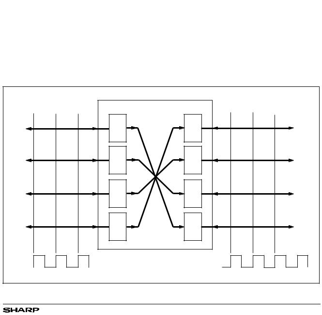
512 x 36 x 2/1024 x 36 x 2 BiFIFOs |
|
|
|
|
|
|
|
LH543611/21 |
|
|
|
|
|
|
|
|
|
|
PARITY CHECKING |
|
|
|
|
|
|
|
|
DA/B35 |
|
|
|
|
DA/B0 |
||
Output word: |
100111100 |
000111100 |
100111000 |
000111000 |
||||
Odd parity: |
Parity of Bytes = 0110; (1 = Byte Parity Error) |
|
|
|
= L |
|||
PF |
||||||||
Even parity: |
Parity of Bytes = 1001; (1 = Byte Parity Error) |
|
= L |
|||||
PF |
||||||||
|
PARITY GENERATION |
|
|
|
|
|
|
|
|
DA/B35 |
|
|
|
|
DA/B0 |
||
Input word: |
100111100 |
000111100 |
100111000 |
000111000 |
||||
Output, odd parity: |
100111100 |
100111100 |
000111000 |
000111000 |
||||
Output, even parity: |
000111100 |
000111100 |
100111000 |
100111000 |
||||
|
|
|
|
|
|
|
|
|
Figure 6. Example of Parity Checking and Generation
|
|
|
|
|
|
Table 2b. Bus Funneling/Defunneling * |
|
|
|
|
|
|
|
|
||||||||
|
|
DA[35:0] |
|
|
WS = 3 (HH) |
|
|
WS = 2 (HL) |
|
|
WS = 1 (LH) |
|
|
|
WS = 0 (LL) |
|||||||
|
|
|
|
|
DB[35:0] |
|
|
DB[35:0] |
|
DB[35:18] |
DB[17:0] |
DB[35:9] |
DB[8:0] |
|||||||||
|
|
|
|
|
|
|
|
|
|
|||||||||||||
0 |
B3 |
B2 |
B1 |
B0 |
0 |
B3 |
B2 |
B1 |
B0 |
B0 |
B1 |
B2 |
B3 |
B3 |
B2 |
B1 |
B0 |
B3 |
B2 |
B1 |
B0 |
|
1 |
B7 |
B6 |
B5 |
B4 |
1 |
B7 |
B6 |
B5 |
B4 |
B4 |
B5 |
B6 |
B7 |
B1 |
B0 |
B3 |
B2 |
B0 |
B3 |
B2 |
B1 |
|
|
|
|
|
|
2 |
|
|
|
|
|
|
|
|
B7 |
B6 |
B5 |
B4 |
B1 |
B0 |
B3 |
B2 |
|
|
|
|
|
|
3 |
|
|
|
|
|
|
|
|
B5 |
B4 |
B7 |
B6 |
B2 |
B1 |
B0 |
B3 |
|
|
|
|
|
|
4 |
|
|
|
|
|
|
|
|
|
|
|
|
|
B7 |
B6 |
B5 |
B4 |
* NOTE: B0, B1, . . ., represent data bytes. |
|
|
|
|
|
|
|
|
|
|
|
|
|
|
|
|
|
|||||
|
INPUT |
|
|
|
LH543611/21 |
|
|
|
|
|
|
|
OUTPUT: WS[1:0]= 2 (HL) |
|
||||||||
|
B3 |
|
B7 |
|
|
DA35 |
|
|
|
|
DB35 |
|
|
B0 |
|
B4 |
|
|
|
|
||
|
BYTE #4 |
BYTE #8 |
|
. |
|
|
|
|
|
. |
|
|
BYTE #1 |
BYTE #5 |
|
|
|
|||||
|
|
|
|
|
|
. . |
|
|
|
|
|
. . |
|
|
|
|
|
|
|
|
|
Bus Example: IBM, Motorala, etc. |
Bus Example: Intel, DEC, etc. |
|
|
|
|
|
DA27 |
|
|
|
|
DB27 |
|
|
|
|
|
|
|
|
|
||
B2 |
|
B6 |
|
|
DA26 |
|
|
|
|
DB26 |
|
|
B1 |
|
B5 |
|
|
|
||||
BYTE #3 |
BYTE #7 |
|
. |
|
|
|
|
|
. |
|
|
BYTE #2 |
BYTE #6 |
|
|
|||||||
|
. . |
|
|
|
|
|
. . |
|
|
|
|
|||||||||||
|
|
|
|
|
|
|
|
|
|
|
|
|
|
|
|
|
|
|
||||
|
|
|
|
|
DA18 |
|
|
|
|
DB18 |
|
|
|
|
|
|
|
|
|
|||
B1 |
|
B5 |
|
|
DA17 |
|
|
|
|
DB17 |
|
|
B2 |
|
B6 |
|
|
|
||||
BYTE #2 |
BYTE #6 |
|
. |
|
|
|
|
|
. |
|
|
BYTE #3 |
BYTE #7 |
|
|
|||||||
|
. . |
|
|
|
|
|
. . |
|
|
|
|
|||||||||||
|
|
|
|
|
|
|
|
|
|
|
|
|
|
|
|
|
|
|
||||
|
|
|
|
|
DA9 |
|
|
|
|
|
DB9 |
|
|
|
|
|
|
|
|
|
||
B0 |
|
B4 |
|
|
DA8 |
|
|
|
|
|
DB8 |
|
|
B3 |
|
B7 |
|
|
|
|||
|
|
|
|
|
|
|
|
|
|
|
|
|
|
|
|
|||||||
|
BYTE #1 |
BYTE #5 |
|
. |
|
|
|
|
|
. |
|
|
BYTE #4 |
BYTE #8 |
|
|
|
|||||
|
|
. . |
|
|
|
|
|
. . |
|
|
|
|
|
|||||||||
|
|
|
|
|
|
|
|
|
|
|
|
|
|
|
|
|
|
|
|
|
||
|
|
|
|
|
|
DA0 |
|
|
|
|
|
DB0 |
|
|
|
|
|
|
|
|
|
|
|
0 |
|
1 |
|
2 |
|
|
|
|
|
|
|
|
|
0 |
|
|
1 |
|
2 |
|
3 |
|
|
|
|
CKA |
|
|
|
|
|
|
|
|
|
|
|
CKB |
|
|
|
|
||
|
|
|
|
|
|
|
|
|
|
|
|
|
|
|
|
|
|
|
|
|
|
543611-52 |
Figure 7. Example of 36-to-36 Byte Order Reversal
15

LH543611/21 |
512 x 36 x 2/1024 x 36 x 2 BiFIFOs |
PORT B WORD-WIDTH SELECTION
PORT
A
36-Bit Data Stream |
|
|
|
18-Bit Data Streams |
|
|
|||||
D35A |
|
|
|
Bits 18-35 |
|
|
|
|
D35B |
|
|
18 |
Bits |
(2nd Halfword) |
|
|
|
18 |
|
2nd Halfword, then 1st Halfword |
|||
|
|
|
|
|
|
|
|||||
|
|
|
|
|
|
|
|||||
|
|
|
|
|
|
|
|
|
|
||
|
|
(2nd |
18- |
35 |
|
|
|
|
|
|
|
D18A |
|
|
Halfword) |
0 |
|
|
D18B |
|
|
||
|
|
|
|
|
-17 |
|
|
|
PORT |
||
|
|
|
|
Bits |
Halfword) |
|
|||||
|
|
|
|
|
|
|
|
|
|
||
|
|
|
|
|
(1st |
|
|
|
|
|
B |
|
|
|
|
|
|
|
|
|
|
|
|
D17A |
|
|
|
|
|
|
|
|
D17B |
|
1st Halfword, then 2nd Halfword |
18 |
|
|
Bits 0-17 |
|
18 |
|
|||||
D0A |
|
|
|
|
|
D0B |
|
||||
|
|
|
|
|
|
||||||
|
|
|
|
|
|
|
|
|
|||
|
|
|
|
|
|
|
|
|
|||
|
|
|
(1st Halfword) |
|
|
|
|
|
|
||
|
|
|
|
|
|
|
|
|
|
|
|
543611-15
Figure 8a. 36-to-18 Funneling Through FIFO #1
36-Bit Data Stream |
9-Bit Data Streams |
|
|||||
D35A |
|
Bits 27-35 |
|
|
|
D35B |
|
|
|
|
|
|
|||
|
9 |
(4th Byte) |
|
|
9 |
|
4th Byte, then 1st Byte, then 2nd Byte, then 3rd Byte |
|
|
|
|
|
|||
D27A |
|
|
|
D27B |
|||
|
|
|
|
|
|
||
|
|
|
|
|
|
||
D26A |
|
Bits 18-26 |
|
|
|
D26B |
|
|
|
|
|
|
|||
|
9 |
(3rd Byte) |
|
|
9 |
|
3rd Byte, then 4th Byte, then 1st Byte, then 2nd Byte |
|
|
|
|
|
|||
D18A |
|
|
|
D18B |
|||
|
|
|
|
|
|
||
|
|
|
|
|
|
||
PORT |
|
|
|
|
|
|
PORT |
A |
|
|
|
|
|
|
B |
D17A |
|
Bits 9-17 |
|
|
|
D17B |
|
|
|
|
|
|
|||
|
9 |
(2nd Byte) |
|
|
9 |
|
2nd Byte, then 3rd Byte, then 4th Byte, then 1st Byte |
|
|
|
|
|
|||
D9A |
|
|
|
D9B |
|||
|
|
|
|
|
|
||
|
|
|
|
|
|
||
D8A |
|
Bits 0-8 |
|
|
|
D8B |
|
|
|
|
|
|
|||
|
9 |
(1st Byte) |
|
|
9 |
|
1st Byte, then 2nd Byte, then 3rd Byte, then 4th Byte |
|
|
|
|
|
|||
D0A |
|
|
|
D0B |
|||
|
|
|
|
|
543611-16 |
||
|
|
|
|
|
|||
|
|
|
|
|
|
|
|
|
|
Figure 8b. |
36-to-9 Funneling Through FIFO #1 |
||||
NOTES:
1.The heavy black borders on register segments indicate the main data path, suitable for most applications. Alternate paths feature a different ordering of bytes within a word, at Port B.
2.The funneling process does not change the ordering of bits within a byte. Halfwords (Figure 8a) or bytes (Figure 8b) are transferred in parallel form from Port A to Port B.
3.The word-width setting may be changed during system operation; however, two clock intervals should be allowed for these signals to settle, before again attempting to read D0B – D35B. Also, incomplete data words may occur, when the word width is changed from shorter to longer at an inappropriate point in the data block passing through the FIFO.
16
512 x 36 x 2/1024 x 36 x 2 BiFIFOs |
LH543611/21 |
PORT B WORD-WIDTH SELECTION
36-Bit Data Stream |
18-Bit Data Stream |
D35A
18
D18A
PORT
A
D17A
18
D0A
Bits |
|
|
(2nd |
18- |
35 |
|
Halfword) |
|
Bits 0-17
(1st Halfword)
D35B
18
D18B
PORT
B
D17B
18 |
1st Halfword, then 2nd Halfword |
D0B
543611-17
|
|
|
Figure 9a. |
18-to-36 Defunneling Through FIFO #2 |
||||
|
|
|
||||||
36-Bit Data Stream |
9-Bit Data Stream |
|
||||||
D35A |
|
|
|
|
|
D35B |
|
|
9 |
|
Bits 27-35 |
|
9 |
|
|||
|
|
|
|
|
|
|||
D27A |
|
|
(4th Byte) |
|
|
D27B |
|
|
|
|
|
|
|
|
|||
|
|
|
|
|
|
|||
D26A |
|
|
Bits 18-26 |
|
|
D26B |
|
|
9 |
|
|
9 |
|
||||
|
|
|
|
|
|
|||
|
|
(3rd Byte) |
|
|
|
|
||
|
|
|
|
|
|
|
|
|
D18A |
|
|
|
|
|
D18B |
|
|
|
|
|
|
|
|
|||
PORT |
|
|
|
|
|
|
PORT |
|
A |
|
|
|
|
|
|
B |
|
D17A |
|
|
Bits 9-17 |
|
|
D17B |
|
|
9 |
|
|
9 |
|
||||
|
|
|
|
|
|
|||
|
|
(2nd Byte) |
|
|
|
|
||
D9A |
|
|
|
|
|
D9B |
|
|
|
|
|
|
|
|
|||
D8A |
|
|
Bits 0-8 |
|
|
D8B |
|
|
9 |
|
|
9 |
1st Byte, then 2nd Byte, then 3rd Byte, then 4th Byte |
||||
|
|
|
|
|
||||
|
|
|
|
|
||||
|
|
|
(1st Byte) |
|
|
|
|
|
D0A |
|
|
|
|
|
D0B |
543611-18 |
|
|
|
|
|
|
||||
|
|
|
|
|
|
|
|
|
|
|
|
Figure 9b. |
9-to-36 Defunneling Through FIFO #2 |
||||
NOTES:
1.The heavy black borders on register segments indicate the only data paths used. The other byte segments of Port B do not participate in the data path during defunneling.
2.The defunneling process does not change the ordering of bits within a byte. Halfwords (Figure 9a) or bytes (Figure 9b) are transferred in parallel form from Port B to Port A.
3.The word-width setting may be changed during system operation; however, two clock intervals should be allowed for these signals to settle, before again attempting to send data. Also, incomplete data words may occur, when the word width is changed from shorter to longer at an inappropriate point in the data block passing through the FIFO.
17

LH543611/21 |
|
|
|
|
|
|
|
|
|
|
|
|
|
|
|
|
|
|
|
512 x 36 x 2/1024 x 36 x 2 BiFIFOs |
|||||||||||||
|
|
|
|
|
Table 3a. LH543611 Resource-Register Programming |
|
|
|
|
|
|
|
|
|
|
||||||||||||||||||
RESOURCE- |
|
|
|
|
|
|
|
|
|
|
|
|
|
|
|
|
|
|
|
|
|
|
|
|
|
|
|
|
|
|
|
||
REGISTER |
|
|
|
|
|
|
|
|
RESOURCE-REGISTER CONTENTS |
|
|
|
|
|
|
|
|
|
|
|
|||||||||||||
ADDRESS |
|
|
|
|
|
|
|
|
|
|
|
|
|
|
|
|
|
|
|
||||||||||||||
|
|
|
|
|
|
|
|
|
|
|
|
|
|
|
|
|
|
|
|
|
|
|
|
|
|
|
|
|
|
|
|||
A2A |
A1A |
A0A |
|
|
|
|
|
|
|
|
|
|
|
|
|
|
|
|
|
|
|
|
|
|
|
|
|
|
|
|
|
|
|
|
|
|
|
|
|
|
|
|
|
|
|
NORMAL FIFO OPERATION |
|
|
|
|
|
|
|
|
|
|
|
||||||||||
|
|
|
D35A |
|
|
|
|
|
|
|
|
|
|
|
|
|
|
|
|
|
|
|
|
|
|
|
|
|
|
D0A |
|||
H |
H |
H |
X... |
|
|
|
|
|
|
|
|
|
|
|
|
|
|
|
|
|
|
|
|
|
|
|
|
|
|
...X |
|||
|
|
|
|
|
|
|
|
|
|
|
|
|
|
|
|
|
|
|
|
|
|
|
|
|
|
|
|
|
|
|
|
|
|
|
|
|
|
|
|
|
|
|
|
|
|
|
|
|
|
|
|
|
MAILBOX |
|
|
|
|
|
|
|
|
|
|
|
|||
|
|
|
D35A |
|
|
|
|
|
|
|
|
|
|
|
|
|
|
|
|
|
|
|
|
|
|
|
|
|
|
D0A |
|||
H |
H |
L |
X... |
|
|
|
|
|
|
|
|
|
|
|
|
|
|
|
|
|
|
|
|
|
|
|
|
|
|
...X |
|||
|
|
|
|
|
|
|
|
|
|
|
|
|
|
|
|
|
|
|
|
|
|
|
|
|
|
|
|
|
|
|
|||
|
|
|
|
|
|
|
|
2, |
|
|
2, |
|
1, |
|
|
|
1 FLAG REGISTER (36-BIT MODE) |
|
|
|
|
|
|
|
|
|
|||||||
|
|
|
|
|
|
AF |
AE |
AF |
AE |
|
|
|
|
|
|
|
|
|
|||||||||||||||
|
|
|
|
D35A . . . D27A |
|
D26A . . . D18A |
|
D17A . . . D9A |
|
|
D8A . . . D0A |
|
|
||||||||||||||||||||
H |
L |
H |
|
|
2 Offset 1 |
|
|
2 Offset 1 |
|
|
1 Offset 1 |
|
|
|
|
|
1 Offset 1 |
|
|
||||||||||||||
|
AF |
AE |
AF |
|
|
AE |
|
|
|||||||||||||||||||||||||
|
|
|
|
|
|
|
|
|
|
|
|
|
|
|
|
|
|
|
|
|
|
|
|
|
|
|
|
|
|
||||
|
|
|
|
|
CONTROL REGISTER: FLAG SYNCHRONIZATION, PARITY CONFIGURATION |
|
|
||||||||||||||||||||||||||
|
|
|
D35A |
|
|
|
|
|
|
|
|
|
|
|
|
D18A |
D17A |
D9A |
D8A |
|
|
|
|
|
|
D1A |
D0A |
||||||
H |
L |
L |
X... |
|
|
|
|
|
|
|
|
|
|
|
|
|
...X |
Port B Control 3 |
Port A Control 3 |
PM 2 |
|||||||||||||
|
|
|
|
|
|
|
|
|
|
|
|
|
|
|
|
|
|
|
|
|
|
|
|
|
|
|
|
|
|
|
|
|
|
|
|
|
|
|
|
|
|
|
|
|
|
|
|
|
|
|
|
|
|
|
|
|
|
||||||||||
|
|
|
|
|
|
|
|
|
|
9-BIT |
AE |
|
1 FLAG OFFSET REGISTER |
|
|
|
|
|
|
|
|
|
|
|
|||||||||
|
|
|
D35A |
|
|
|
|
|
|
|
|
|
|
|
|
|
|
|
|
|
|
D9A |
|
|
|
D8A . . . D0A |
|
|
|||||
L |
H |
H |
X... |
|
|
|
|
|
|
|
|
|
|
|
|
|
|
|
|
|
|
...X |
|
|
|
1 Offset 1 |
|
|
|||||
|
|
|
|
|
|
|
|
|
|
|
|
|
|
|
|
|
|
|
AE |
|
|
||||||||||||
|
|
|
|
|
|
|
|
|
|
|
|
|
|
|
|
|
|
|
|
|
|
|
|
|
|
|
|
|
|
|
|
|
|
|
|
|
|
|
|
|
|
|
|
|
|
|
|
|
|
|
|
|
|
|
|
|
|||||||||||
|
|
|
|
|
|
|
|
|
|
9-BIT |
AF |
1 FLAG OFFSET REGISTER |
|
|
|
|
|
|
|
|
|
|
|
||||||||||
|
|
|
D35A |
|
|
|
|
|
|
|
|
|
|
|
|
|
|
|
|
|
|
D9A |
|
|
|
D8A . . . D0A |
|
|
|||||
L |
H |
L |
X... |
|
|
|
|
|
|
|
|
|
|
|
|
|
|
|
|
|
|
..X |
|
|
|
1 Offset 1 |
|
|
|||||
|
|
|
|
|
|
|
|
|
|
|
|
|
|
|
|
|
|
|
AF |
|
|
||||||||||||
|
|
|
|
|
|
|
|
|
|
|
|
|
|
|
|
|
|
|
|
|
|
|
|
|
|
|
|
|
|
|
|
|
|
|
|
|
|
|
|
|
|
|
|
|
|
|
|
|
|
|
|
|
|
|
|
||||||||||||
|
|
|
|
|
|
|
|
|
|
9-BIT |
AE |
2 FLAG OFFSET REGISTER |
|
|
|
|
|
|
|
|
|
|
|
||||||||||
|
|
|
D35A |
|
|
|
|
|
|
|
|
|
|
|
|
|
|
|
|
|
|
D9A |
|
|
|
D8A . . . D0A |
|
|
|||||
L |
L |
H |
X... |
|
|
|
|
|
|
|
|
|
|
|
|
|
|
|
|
|
|
...X |
|
|
|
2 Offset 1 |
|
|
|||||
|
|
|
|
|
|
|
|
|
|
|
|
|
|
|
|
|
|
|
AE |
|
|
||||||||||||
|
|
|
|
|
|
|
|
|
|
|
|
|
|
|
|
|
|
|
|
|
|
|
|
|
|
|
|
|
|
|
|
|
|
|
|
|
|
|
|
|
|
|
|
|
|
|
|
|
|
|
|
|
|
|
|
||||||||||||
|
|
|
|
|
|
|
|
|
|
9-BIT |
AF |
2 FLAG OFFSET REGISTER |
|
|
|
|
|
|
|
|
|
|
|
||||||||||
|
|
|
D35A |
|
|
|
|
|
|
|
|
|
|
|
|
|
|
|
|
|
|
D9A |
|
|
|
D8A . . . D0A |
|
|
|||||
L |
L |
L |
X... |
|
|
|
|
|
|
|
|
|
|
|
|
|
|
|
|
|
|
...X |
|
|
|
2 Offset 1 |
|
|
|||||
|
|
|
|
|
|
|
|
|
|
|
|
|
|
|
|
|
|
|
AF |
|
|
||||||||||||
NOTES:
1.All four programmable-flag-offset values are initialized to eight (8) during a reset operation.
2.Parity Mode: Odd parity = HIGH; even parity = LOW. The parity mode is initialized to odd during a reset operation.
3.See Tables 5 and 6 and Figure 10 for the detailed format of the Control Register word.
18
 Loading...