

Page 1

PLASMA DISPLAY TV
Chassis : D53A(P)
Model: PS42P2SDX/XEC
PLASMA DIAPLAY TV CONTENTS
Precautions
Reference Information
Specifications
Alignment and Adjustments
Circuit Operation Description
Troubleshooting
Exploded View and Parts List
Electric Parts List
Handling Description
Glossary
Wiring Diagram
Schematic Diagrams
1.
2.
3.
4.
5.
6.
7.
8.
9.
10.
11.
12.
Page 2

1. Precautions
1-1 Safety Precautions
1. Be sure that all of the built-in protective
devices are replaced. Restore any missing
protective shields.
2. When reinstalling the chassis and its
assemblies, be sure to restore all protective
devices, including: nonmetallic control knobs
and compartment covers.
3. Make sure that there are no cabinet openings
through which people—particularly
children—might insert fingers and contact
dangerous voltages. Such openings include
the spacing between fornt cabinet and back
cabinet, excessively wide cabinet
ventilation slots, and improperly fitted back
covers.
4. Leakage Current Hot Check (Figure 1-1):
Warning: Do not use an isolation
transformer during this test. Use a leakagecurrent tester or a metering system that
complies with American National Standards
Institute (ANSI C101.1, Leakage Current for
Appliances), and Underwriters Laboratories
(UL Publication UL1950.5.2).
5. With the unit completely reassembled, plug
the AC line cord directly into the power
outlet. With the unit’s AC switch first in the
ON position and then OFF, measure the
current between a known earth ground (metal
water pipe, conduit, etc.) and all exposed
metal parts, including: antennas, handle
brackets, metal cabinets, screwheads and
control shafts. The current measured should
not exceed 3.5 milliamp. Reverse the powerplug prongs in the AC outlet and repeat the
test.
Fig. 1-1 AC Leakage Test
6. Antenna Cold Check:
With the unit’s AC plug disconnected from the
AC source, connect an electrical jumper across
the two AC prongs. Connect one lead of the
ohmmeter to an AC prong. Connect the other
lead to the coaxial connector.
7. High Voltage Limits:
High voltage must be measured each time servicing is done on the B+, horizontal deflection
or high voltage circuits.
Precautions
Samsung Electronics 1-1
LEAKAGE
CURRENT
TESTER
DEVICE
UNDER
TEST
TEST ALL
EXPOSED METAL
SURFACES
2-WIRE CORD
ALSO TEST WITH
PLUG REVERSED
(USING AC ADAPTER
PLUG AS REQUIRED)
EARTH
GROUND
(READING SHOULD
NOT BE ABOVE
0.5mA)
Follow these safety, servicing and ESD precautions to prevent damage and protect against potential
hazards such as electrical shock and X-rays.
Page 3

1-2 Safety Precautions (Continued)
8. High voltage is maintained within specified
limits by close-tolerance, safety-related
components and adjustments. If the high
voltage exceeds the specified limits, check
each of the special components.
9. Design Alteration Warning:
Never alter or add to the mechanical or
electrical design of this unit. Example: Do not
add auxiliary audio or video connectors. Such
alterations might create a safety hazard. Also,
any design changes or additions will void the
manufacturer’s warranty.
10. Hot Chassis Warning:
Some TV receiver chassis are electrically
connected directly to one conductor of the AC
power cord. If an isolation transformer is not
used, these units may be safely serviced only
if the AC power plug is inserted so that the
chassis is connected to the ground side of the
AC source.
To confirm that the AC power plug is inserted
correctly, do the following: Using an AC
voltmeter, measure the voltage between the
chassis and a known earth ground. If the
reading is greater than 1.0V, remove the AC
power plug, reverse its polarity and reinsert.
Re-measure the voltage between the chassis
and ground.
11. Some TV chassis are designed to operate with
85 volts AC between chassis and ground,
regardless of the AC plug polarity. These units
can be safely serviced only if an isolation
transformer inserted between the receiver and
the power source.
12. Some TV chassis have a secondary ground
system in addition to the main chassis ground.
This secondary ground system is not
isolated from the AC power line. The two
ground systems are electrically separated by
insulating material that must not be defeated
or altered.
13. Components, parts and wiring that appear to
have overheated or that are otherwise
damaged should be replaced with parts that
meet the original specifications. Always
determine the cause of damage or overheating, and correct any potential hazards.
14. Observe the original lead dress, especially
near the following areas: Antenna wiring,
sharp edges, and especially the AC and high
voltage power supplies. Always inspect for
pinched, out-of-place, or frayed wiring. Do
not change the spacing between components
and the printed circuit board. Check the AC
power cord for damage. Make sure that leads
and components do not touch thermally hot
parts.
15. Product Safety Notice:
Some electrical and mechanical parts have
special safety-related characteristics which
might not be obvious from visual inspection.
These safety features and the protection they
give might be lost if the replacement component differs from the original—even if the
replacement is rated for higher voltage,
wattage, etc.
Components that are critical for safety are
indicated in the circuit diagram by shading,
( ) or ( ).
Use replacement components that have the
same ratings, especially for flame resistance
and dielectric strength specifications.
A replacement part that does not have the
same safety characteristics as the original
might create shock, fire or other hazards.
Precautions
1-2 Samsung Electronics
!
Page 4

1-3 Servicing Precautions
1. Servicing precautions are printed on the
cabinet. Follow them.
2. Always unplug the unit’s AC power cord from
the AC power source before attempting to: (a)
Remove or reinstall any component or
assembly, (b) Disconnect an electrical plug or
connector, (c) Connect a test component in
parallel with an electrolytic capacitor.
3. Some components are raised above the printed
circuit board for safety. An insulation tube or
tape is sometimes used. The internal wiring is
sometimes clamped to prevent contact with
thermally hot components. Reinstall all such
elements to their original position.
4. After servicing, always check that the screws,
components and wiring have been correctly
reinstalled. Make sure that the portion around
the serviced part has not been damaged.
5. Check the insulation between the blades of the
AC plug and accessible conductive parts
(examples: metal panels, input terminals and
earphone jacks).
6. Never defeat any of the B+ voltage interlocks.
Do not apply AC power to the unit (or any of
its assemblies) unless all solid-state heat sinks
are correctly installed.
7. Always connect a test instrument’s ground
lead to the instrument chassis ground before
connecting the positive lead; always remove
the instrument’s ground lead last.
8. Plasma display panels have partial afterimages when a same picture continues to be displayed for a certain time. This happens due to
the degradation of brightness caused by a
scale-down effect.
To prevent such afterimages when displaying
a same picture for a certain time, be sure to
reduce the level of brightness and contrast.
ex) Contrast : 50 or 75, Brightness : 25
9. Plasma display is an array of pixels(cells).
Therefore, if at least 99.9% pixels keep normal,
the appropriate panel is judged as ‘approved
product.’ Even though some of pixels keep
luminescent or always light off, do not worry
because the panel is approved.
Precautions
Samsung Electronics 1-3
Warning 1 : First read the “Safety Precautions” section of this manual. If some unforeseen circumstance creates a
conflict between the servicing and safety precautions, always follow the safety precautions.
Warning 2 : An electrolytic capacitor installed with the wrong polarity might explode.
Page 5

1-4 Precautions for Electrostatically Sensitive Devices (ESDs)
1. Some semiconductor (“solid state”) devices
are easily damaged by static electricity. Such
components are called Electrostatically
Sensitive Devices (ESDs); examples include
integrated circuits and some field-effect
transistors. The following techniques will
reduce the occurrence of component damage
caused by static electricity.
2. Immediately before handling any semicon
ductor components or assemblies, drain the
electrostatic charge from your body by
touching a known earth ground. Alternatively,
wear a discharging wrist-strap device. (Be
sure to remove it prior to applying power—
this is an electric shock precaution.)
3. After removing an ESD-equipped assembly,
place it on a conductive surface such as
aluminum foil to prevent accumulation of
electrostatic charge.
4. Do not use freon-propelled chemicals. These
can generate electrical charges that damage
ESDs.
5. Use only a grounded-tip soldering iron when
soldering or unsoldering ESDs.
6. Use only an anti-static solder removal device.
Many solder removal devices are not rated as
“anti-static”; these can accumulate sufficient
electrical charge to damage ESDs.
7. Do not remove a replacement ESD from its
protective package until you are ready to
install it. Most replacement ESDs are
packaged with leads that are electrically
shorted together by conductive foam,
aluminum foil or other conductive materials.
8. Immediately before removing the protective
material from the leads of a replacement ESD,
touch the protective material to the chassis or
circuit assembly into which the device will be
installed.
9. Minimize body motions when handling
unpackaged replacement ESDs. Motions such
as brushing clothes together, or lifting a foot
from a carpeted floor can generate enough
static electricity to damage an ESD.
Precautions
1-4 Samsung Electronics
Page 6

Reference Information
Samsung Electronics 2-1
2. Reference Information
2-1 Tables of Abbreviations and Acronyms
A
Ah
Å
dB
dBm
°C
°F
°K
F
G
GHz
g
H
Hz
h
ips
kWh
kg
kHz
kΩ
km
km/h
kV
kVA
kW
I
MHz
Ampere
Ampere-hour
Angstrom
Decibel
Decibel Referenced to One
Milliwatt
Degree Celsius
Degree Fahrenheit
degree Kelvin
Farad
Gauss
Gigahertz
Gram
Henry
Hertz
Hour
Inches Per Second
Kilowatt-hour
Kilogram
Kilohertz
Kilohm
Kilometer
Kilometer Per Hour
Kilovolt
Kilovolt-ampere
Kilowatt
Liter
Megahertz
MV
MW
MΩ
m
µA
µF
µH
µm
µs
µW
mA
mg
mH
mI
mm
ms
mV
nF
Ω
pF
Ib
rpm
rps
s
V
VA
W
Wh
Megavolt
Megawatt
Megohm
Meter
Microampere
Microfarad
Microhenry
Micrometer
Microsecond
Microwatt
Milliampere
Milligram
Millihenry
Milliliter
Millimeter
Millisecond
Millivolt
Nanofarad
Ohm
Picofarad
Pound
Revolutions Per Minute
Revolutions Per Second
Second (Time)
Volt
Volt-ampere
Watt
Watt-hour
Table 2-1 Abbreviations
Page 7

Reference Information
2-2 Samsung Electronics
Table 2-2 Table of Acronyms
ABL
AC
ACC
AF
AFC
AFT
AGC
AM
ANSI
APC
APC
A/V
AVC
BAL
BPF
B-Y
CATV
CB
CCD
CCTV
Ch
CRT
CW
DC
DVM
EIA
ESD
ESD
FBP
FBT
FF
FM
FS
GND
G-Y
H
HF
HI-FI
IC
IC
IF
Automatic Brightness Limiter
Alternating Current
Automatic Chroma Control
Audio Frequency
Automatic Frequency Control
Automatic Fine Tuning
Automatic Gain Control
Amplitude Modulation
American National Standards Institute
Automatic Phase Control
Automatic Picture Control
Audio-Video
Automatic Volume Control
Balance
Bandpass Filter
Blue-Y
Community Antenna Television (Cable TV)
Citizens Band
Charge Coupled Device
Closed Circuit Television
Channel
Cathode Ray Tube
Continuous Wave
Direct Current
Digital Volt Meter
Electronics Industries Association
Electrostatic Discharge
Electrostatically Sensitive Device
Feedback Pulse
Flyback Transformer
Flip-Flop
Frequency Modulation
Fail Safe
Ground
Green-Y
High
High-Frequency
High Fidelity
Inductance-Capacitance
Integrated Circuit
Intermediate Frequency
I/O
L
L
LED
LF
MOSFET
MTS
NAB
NEC
NTSC
OSD
PCB
PLL
PWM
QIF
R
RC
RF
R-Y
SAP
SAW
SIF
SMPS
S/N
SW
TP
TTL
TV
UHF
UL
UV
VCD
VCO
VCXO
VHF
VIF
VR
VTR
VTVM
TR
Input/output
Left
Low
Light Emitting Diode
Low Frequency
Metal-Oxide-Semiconductor-Field-Effect-Tr
Multi-channel Television Sound
National Association of Broadcasters
National Electric Code
National Television Systems Committee
On Screen Display
Printed Circuit Board
Phase-Locked Loop
Pulse Width Modulation
Quadrature Intermediate Frequency
Right
Resistor & Capacitor
Radio Frequency
Red-Y
Second Audio Program
Surface Acoustic Wave(Filter)
Sound Intermediate Frequency
Switching Mode Power Supply
Signal/Noise
Switch
Test Point
Transistor Transistor Logic
Television
Ultra High Frequency
Underwriters Laboratories
Ultraviolet
Variable-Capacitance Diode
Voltage Controlled Oscillator
Voltage Controlled Crystal Oscillator
Very High Frequency
Video Intermediate Frequency
Variable Resistor
Video Tape Recorder
Vacuum Tube Voltmeter
Transistor
Page 8

Specifications
Samsung Electronics 3-1
3. Specifications
MODEL
SCREEN SIZE
3-1 Display(PDP Monitor)
Display
Remote Control
Display
Remote Control
Front
Back
Power Supply
Power Consumption
Screen Size
Adjustment System
Dimensions
(mm/inch)
Terminal
In/Out
Terminals
PS-42P2S
16:9
1039(W) x 89(D) x 635(H)/40.9(W) x 3.5(D) x 25(H)
54(W) x 31.5(D) x 220(H)/2.13(W) x 1.24(D) x 8.66(H)
32Kg/70.54\bs
150g/0.33\bs
POWER , MUTE, -VOLME+, ▲SELECT▼, MENU,SOURCE
AV1(S-VHS IN, VIDEO IN)
AV2(SCART IN)
PC IN
AUDIO IN(AV1, PC)
RS232C(only for service)
External Speaker Out
AC220V 50/60Hz
350W
852 x 474(106 cm)/33.54 x 18.66(42inchs)
Electronic Function Adjustment
Page 9

3-2 Samsung Electronics
MENO
Page 10

Alignment and Adjustments
Samsung Electronics 4-1
4. Alignment and Adjustments
4-1 Service Mode
4-1-1 SERVICE MODE ENTRY METHOD (General Transmitter)
1. Turn off the power to make the SET STAND-BY mode.
2. In order to enter the Service Mode, select MUTE-1-8-2-POWER.
✳ In case entry into SERVICE MODE is unsuccessful, repeat the procedures above.
4-1-2 Initial DISPLAY State in times of SERVICE MODE Switch overs
4-1-2(A) OSD DISPLAY
4-1-2(B) BUTTONS OPERATIONS WITHIN SERVICE MODE
#Notice
1. In case of no signal in ALL MODE. entry into the FACTORY MODE cannot be made.
1. PWS364A 9. PinP Control
2. VPC3230 10. OSD Position
3. SDA9400 11. Test Position
4. SDA9280 12. Option Table
5. AD9884-Video 13. Reset
6. AD9884-DTV/PC
7. CXA2101Q-1
8. CXA2101Q-2
Release Time :
Menu
Joystick UP/DOWN
Joystick
Entire menu display
Cursor move to select items
Enable to increase and decrease the data of the selected items
Page 11

Alignment and Adjustments
4-2 Samsung Electronics
4-1-3 Details of Control
4-1-3(A) PW364A
No OSD Item Range Default Description
1
2
3
4
5
6
7
8
9
10
11
12
13
14
15
16
H Position
V Position
Red Gain
Green Gain
Blue Gain
Red offset
Green offset
Blue offset
APL on/off
High Light
Low Light
Shift Pixel
Test
Pixel Number
Shift Line
Time
H Position
V Position
Red Gain
Green Gain
Blue Gain
Red Cutoff
Green Cutoff
Blue Cutoff
APL on/off
High Light
Low Light
Shift Pixel
Test
Pixel Number
Shift Live
Time
0 ~ 127
0 ~ 84
0 ~ 255
0 ~ 255
0 ~ 255
0 ~ 255
0 ~ 255
0 ~ 255
0, 1
0 ~ 255
0 ~ 255
off, on
0,1
0 ~ 5
0 ~ 5
0 ~ 60
30
34
116
116
116
128
128
128
1
116
128
Off
0
4
4
4
H-Position(The Picture moves left when the value increase)
V-Position(The Picture moves up when the value increase)
High Light Adjustment(Variable)
High Light Adjustment(Variable)
High Light Adjustment(Fixed)
Low Light Adjustment(Variable)
Low Light Adjustment(Variable)
Low Light Adjustment(Fixed)
Fixed, Shipment Setting : APL On
4-1-3(B) VPC3230
No OSD Item Range Default Description
1
2
3
4
5
6
7
8
9
10
11
12
13
Bright YUV
Cont YUV
IF Comp
Chroma band
Ena Luma
HPLL Speed
Luma Delay
3230 Bright
3230 Contrast
H LPF Y/C
H LPF Chroma
H Peaking
Coaring Off/On
Brightness of YUV
Contrast of YUV
IF Compensation
Chroma band width
Enable Luma, LPF
HPLL Speed
Luma/Chroma Delay
Brightness
Contrast
H LPF for Y/C
H LPF Chroma
H Peaking Filter
Coaring Off/On
0 ~ 255
0 ~ 63
0 ~ 3
0 ~ 4
0 ~ 1
0 ~ 3
0 ~ 9
0 ~ 255
0 ~ 63
0 ~ 4
0 ~ 2
0 ~ 3
0, 1
195
27
2
3
1
1
5
168
36
0
0
2
1
Comp, (DVD) Bright, Level (Fixed)
Comp, (DVD) Cont, Level (Fixed)
Air IF Frequency Characteristic Setting (Fixed)
Chroma Band Setting (Fixed)
Determines whether LPF is used or not (Fixed)
VCR/Air Sync, Response Velocity Setting
Y/C Delay
By pass, f1, f2, f3
Board, Med, Narrow
Coaring off, on
Page 12

Alignment and Adjustments
Samsung Electronics 4-3
4-1-3(C) SDP9400
No OSD Item Range Default Description
1
2
3
4
5
6
SNR On
VCSNR On
HCSNR On
DTNR On
TNRCLY
TNRCNC
SNR On
VCSNR On
HCSNR On
DTNR On
TNRCLY
TNRCNC
0, 1
0, 1
0, 1
0, 1
0 ~ 15
0 ~ 15
1
1
0
1
5
5
Spatial Noise Reduction
Vertical Spatial Noise Reduction
Horiz, Spatial Noise Reduction
Frame/Field Selection
4-1-3(D) SDA9280
No OSD Item Range Default Description
1
2
3
4
5
6
7
8
CTI Thresh
CTI Trawid
Y-Delay
LPF Gain
BPF Gain
HPF Gain
Phacom
Cor
CTI Thresh
CTI Trawid
Y-Delay
LPF Gain
BPF Gain
HPF Gain
Phacom
Cor
0 ~ 15
0 ~ 15
0 ~ 15
0 ~ 7
0 ~ 15
0 ~ 15
0 ~ 3
0, 1
0
0
11
4
8
8
0
1
4-1-3(E) AD9884-VIDEO
No OSD Item Range Default Description
1
2
3
4
5
6
Red Gain
Green Gain
Blue Gain
Red Offset
Green Offset
Blue Offset
Red Gain
Green Gain
Blue Gain
Red Offset
Green Offset
Blue Offset
0 ~ 255
0 ~ 255
0 ~ 255
0 ~ 63
0 ~ 63
0 ~ 63
137
128
141
27
32
36
PC Mode W/B (Fixed)
PC Mode W/B (Fixed)
PC Mode W/B (Fixed)
PC Mode W/B (Fixed)
PC Mode W/B (Fixed)
PC Mode W/B (Fixed)
Page 13

Alignment and Adjustments
4-4 Samsung Electronics
4-1-3(F) AD9884 DTV/PC
No OSD Item Range Default Description
1
2
3
4
5
6
7
8
9
10
11
12
13
14
15
16
17
Sub Bright
Limit Level
System
D-Color
R Drive
G Drive
B Drive
R CutOff
G CutOff
B CutOff
ABL Mode
ABL TH
H Sep Sel.
Fix Sync.
V Time Con
H Width
HHD timi Con
Sub Bright
Limit Level
System
D-Color
R Drive
G Drive
B Drive
R CutOff
G CutOff
B CutOff
ABL Mode
ABL-TH
H Sep Sel.
Fix Sync.
V Time Constant
H Width
H timi Constant
0 ~ 63
0 ~ 3
0 ~ 3
0 ~ 2
0 ~ 63
0 ~ 63
0 ~ 63
0 ~ 63
0 ~ 63
0 ~ 63
0 ~ 3
0 ~ 3
0, 1
0 ~ 3
0 ~ 3
0 ~ 3
0, 1
51
0
1
1
32
32
32
32
32
32
0
0
0
0
1
1
0
Limits the input level (Fixed)
480p, 720p, 1080i
Dynamic Color
DTV W/B (Fixed)
DTV W/B (Fixed)
DTV W/B (Fixed)
DTV W/B (Fixed)
DTV W/B (Fixed)
DTV W/B (Fixed)
ABL Mode Setting
Voltage
H-Sync, Seperation System
0 : Auto
Set the time constant for V-Sync Seperation
H-Sync Width Adjustment
4-1-3(G) CXA2101Q-1
No OSD Item Range Default Description
1
2
3
4
5
6
Red Gain
Green Gain
Blue Gain
Red Offset
Green Offset
Blue Offset
Red Gain
Green Gain
Blue Gain
Red Offset
Green Offset
Blue Offset
0 ~ 255
0 ~ 255
0 ~ 255
0 ~ 63
0 ~ 63
0 ~ 63
125
128
127
40
32
39
PC Mode W/B (Fixed)
PC Mode W/B (Fixed)
PC Mode W/B (Fixed)
PC Mode W/B (Fixed)
PC Mode W/B (Fixed)
PC Mode W/B (Fixed)
Page 14

Alignment and Adjustments
Samsung Electronics 4-5
4-1-3(H) CXA2101QQ-2
No OSD Item Range Default Description
1
2
3
4
5
6
7
8
9
10
11
12
13
14
15
16
HS Mask
Sub Cont
Sub Color
Sub Hue
Sub SHP
R-Y/R
R-Y/B
G-Y/R
G-Y/B
PABL Level
SHP FO
Pre/over
CTI Level
LTI Level
DC-Tran
D-Pic
HS Mask
Sub Contrast
Sub Color
Sub Hue
Sub SHP
R-Y/R
R-Y/B
G-Y/R
G-Y/B
PABL Level
SHP FO
Pre/over
CTI Level
LTI Level
DC-Tran
D-Pic
0, 1
0 ~ 15
0 ~ 15
0 ~ 15
0 ~ 4
0 ~ 15
0 ~ 15
0 ~ 15
0 ~ 15
0 ~ 15
0 ~ 4
0 ~ 3
0 ~ 3
0 ~ 3
0 ~ 3
0 ~ 3
1
7
5
8
2
13
15
8
4
8
2
3
1
0
1
1
13 (PAL), 5(NT)
4 (PAL), 8 (NT)
Peak ABL
Sharpness FO Selection
0=Pre. : Over=1:1.3 3=3:1
C Transition Level
Y Transition Level
Y DC Transmission Rate
Dynamic Picture
4-1-3(I) PINP CONTROL
No OSD Item Range Default Description
1
2
3
4
5
6
7
PIP HPos
PIP VPos
Bright YUV
Cont YUV
Luma Delay
3230 Bright
3230 Contrast
PIP HPos
PIP VPos
Bright YUV
Cont YUV
Luma Delay
3230 Bright
3230 Contrast
0 ~ 63
0 ~ 63
0 ~ 255
0 ~ 63
0
0 ~ 63
0 ~ 63
6
13
195
27
0
40
38
PinP Horizontal Position
PinP Vertical Position
Comp. Bright. Level (Fixed)
Comp. Bright. Level (Fixed)
Y/C Delay
Page 15

Alignment and Adjustments
4-6 Samsung Electronics
4-1-3(J) OSD POSITION
No OSD Item Range Default Description
1
2
Horiz
Vert
Horiz(Left, Right)
Vert(Up, Down)
8 ~ 104
8 ~ 40
10440Move 8 by 8 (Total : 12 Step), Fixed
Move 8 by 8 (Total : 4 Step), Fixed
No OSD Range Default Description
1
2
3
4
5
6
7
8
Pseudo Color Bar
Luma Ramp
White 16
White 90
White 240
Red
Green
Blue
0 ~ 15
0 ~ 15
0 ~ 15
0 ~ 7
0 ~ 15
0 ~ 15
0 ~ 3
0, 1
-
-
-
-
-
-
-
-
4-1-3(K) TEST PATTERN
No ITEM Default Description
1
2
3
4
5
6
7
Rear Jack
Blue Screen
Picture Size-Aspect
Frame Lock
Remocon Pin
Pivot
Panel Life Time
Scart
30
Last Memory
On
01
On
-
Scart <--> RCA
0 → 5 → 10 → 15 → 20 → 25 → 30 → 0
Wide <--> Last Memory
On <--> Off
00 ~ 99
On <--> Off
Indicate total elapsed time
4-1-3(L) OPTION TABLE
Page 16

Samsung Electronics 4-7
Alignment and Adjustments
4-1-4 White Balance Adjust Method
1. Press MUTE-1-8-2-POWER to enter the factory mode.
2. Enter PW364A.
3. Adjust LOW coordinates as R, G, OFFSET and HIGH coordinates as R, G, GAIN.(Blue is fixed)
4. Adjust LOW light as Center Offset.
5. Adjust HIGH light as Gain Max.
6. Adjust fine as B-Offset and B-Gain.
- W/B Adjustment SPEC(Suwon Factory Toshiba PATTERN)
➣ VIDEO MODE
➣ PC MODE
Adjustment
Coordinates
H-LIGHT
L-LIGHT
Coordinates
Value
x : 282
y : 296
Y : 24.5[f\]
x : 282
y : 296
Y : 0.95[f\]
Adjustment
Deviation
±: 3
±: 3
±: 1
±: 5
±: 5
± : 0.1
Adjustment
Coordinates
H-LIGHT
L-LIGHT
Coordinates
Value
x : 282
y : 296
Y : 15[f\]
x : 282
y : 296
Y : 0.33[f\]
Adjustment
Deviation
±: 3
±: 3
±: 1
±: 5
±: 5
± : 0.05
Page 17

4-8 Samsung Electronics
Alignment and Adjustments
SPK4215M PC
USER
V-Position
Factory
HP/VP/P
PHASE
CLOCK/
fO(Hz)
125/22/0/0
125/16/0/0
125/22/0/0
125/16/0/0
70.1
70.0
125/8/0/1
124/31/0/0
125/8/0/1
124/31/0/0
85
75
125/2/0/0
125/31/0/0
125/2/0/0
125/31/0/0
72.8
59.9
125/9/1/2
125/0/0/1
125/9/1/2
125/0/0/1
75
85.1
125/31/0/2
125/15/0/1
125/31/0/2
125/15/0/1
72.2
60.3
126/1/0/1
126/14/2/3
126/1/0/1
126/14/2/3
85
56.3
125/20/1/3
125/21/1/3
125/20/1/3
125/21/1/3
75
70.1
125/16/1/2
125/16/1/2
60
HFreqSec
/99=31.777
/99=31.777
HS1Period
31.777u/10.1n=3146.2
31.777u/10.1n=3146.2
Dot_c
V_P
H_P
VTotal
28.232
1
0
449
31.777
25.175
0
1
449
31.777
HFreqSes
=23.111
=26.666
=2288.21
=2640.29
36.0
31.5
0
0
0
0
509
500
23.111
26.667
=26.414
=31.777
=2615.14
=3146.23
31.5
25.175
0
0
0
0
520
525
26.413
31.777
=18.626
=21.333
=1844.65
=2112.17
49.5
56.25
1
1
1
1
631
625
18.631
21.333
=20.797
=26.393
=2059.4
=2613.86
50.0
40.0
1
1
1
1
666
628
20.800
26.400
=28.444
=14.555
=2816.23
=1441.68
36.0
94.5
1
1
625
808
28.444
14.561
=16.656
=17.707
=1649.50
=1753.16
78.75
75.000
1
0
1
0
800
806
16.660
17.707
=20.676
=2047.22
65.000
0
0
806
20.677
400
350
480
480
480
480
600
600
600
600
600
768
768
768
1024
14
768
1024
15
VRes
720
640
640
640
640
640
800
800
800
800
800
1024
12
1024
13
HRes
1
2
3
4
5
6
7
8
9
10
NO
11
Page 18

Samsung Electronics 4-9
Alignment and Adjustments
4-3 Discharge Voltage Adjustment Method (Monitor) in Times of ASS’Y Repair
and Replacement
-All VR (Variable Resistor), except for VR for Vs, voltage goes down when turned counterclockwise.
● Vsc and Vy Adjustment Method
● Vs and Va Adjustment Method
■ Vsc is the voltage of the left terminal
for D5207
■ Voltage adjustment is made for Vsc by
using VR5201
■ Standard voltage for Vsc is –55V±10V
■ Vy is the voltage of the right terminal
for D5207
■ Voltage adjustment is made for Vy by
using VR5200
■ Standard voltage for Vy is 132V±10V
■ Vs is the voltage of the no.11 PIN of
SX Connector.
■ Voltage adjustment is made for Vs by
using VR in 7
■ Vs is 175±5V
■ Va is the voltage of the no.7 PIN of SX
Connector.
■ Voltage adjustment is made for Va by
using right VR in 6
■ Va is 75±5V
Y-Main
Page 19

4-10 Samsung Electronics
Alignment and Adjustments
● Vw Adjustment Method
■ Vw is the voltage of the right terminal
for R4414
■ Voltage adjustment is made for Vw by
using VR4400
■ Standard voltage for Vw is 175V±5V
Page 20

Samsung Electronics 4-11
Alignment and Adjustments
4-4 Fault Finding Using MULTI METER
Parts defects can be found for DIODE TRANSISTOR IC, using MULTI TEST including
Forward/Reverse direction Multi Test. Of course, in case resistance of several ohms and COIL are connected in parallel circuit, the lock out circuit parallel connected to part must be severed.
1.DIODE
2. TRANSISTOR
● For NPN(KSC815-Y, 2SC2068, 2SC2331-Y)
● For PNP(KSA539-Y)
Forward Direction
Hundreds of ohms
Reverse Direction
Infinity
Between Anode and Cathode
C (COLLECTOR)
E
B(BASE)
BC
C (COLLECTOR)
E
B(BASE)
BC
E (EMITTER)
E (EMITTER)
Forward Direction
Hundreds of ohms
Hundreds of ohms
Infinity
Reverse Direction
Infinity
Infinity
Infinity
Between B and E
Between B and C
Between E and C
Forward Direction
Hundreds of ohms
Hundreds of ohms
Infinity
Reverse Direction
Infinity
Infinity
Infinity
Between B and E
Between B and C
Between E and C
+- +-
Page 21

4-12 Samsung Electronics
Alignment and Adjustments
3. IC (INTEGRATED CIRCUIT)
IC has built in DIODE against overvoltage in PIN. Generally, except for internal circuit defects, IC defects
can be found, by measuring the DIODE.
✴ Defects have SHORT(0 ohm) for both forward and reverse direction.
Hundreds of ohms
Forward Direction
Reverse Direction
Varying depending on IC but generally normal
Infinity in DIODE TEST MODE
Page 22

Circuit Operation Description
Samsung Electronics 5-1
5. Circuit Description
5-1 Power supply
5-1-1 Outline(PDP SMPS)
Considering various related conditions, the switching regulator with good efficiency and allowing for its
small size and lightweight was used as the power supply for PDP. Most of the power supply components
used forward converter, and Vsamp and Vsb used simple flyback converter.
To comply with the international harmonics standards and improve the power factor, active PFC (Power
Factor Correction) was used to rectify AC input into +400V DC output, which in turns used as input to the
switching regulator.
5-1-2 42"SD SMPS SPECIFICATION
5-1-2(A) INPUT
PDP-42PS board is designed so that input power can be used within AC 90 VAC to 264 VAC with
50/60Hz ± 3Hz.
5-1-2(B) OUTPUT
PDP-42PS board provides 13 output switching power supplies for PDP 50inch (+165Vs, +220Set, +185Ve,
+75Va, +80Scan, +18Vg, +5Vsb, +5V(D), +5V(A), +12V. +9V, +12Vfan, and +12Vsamp). The output voltage, and current requirements for continuous operation are stated below (Table 3).
Table1. Specifications of Output Power Supplies for PDP SMPS
Output Name
Vs
Va
Vscan
Vset
Ve
Vg
Vfan
V9
V5(A)
V5(D)
Vsb
V12
Vsamp
Output Voltage
+165V
+75V
+80V
+220V
+185V
+18.3V
+12V
+9V
+5V
+5.3V
+5V
+12V
+12V
Output Current
1.4A
0.5A
0.05A
0.05A
0.05A
0.3A
0.8A
0.3A
1.0A
3.5A
0.4
1.2A
1.5A
Using in PDP driving
Sustain Voltage of Drive Board
Address Voltage of Drive Board
Analog IC Drive Voltage of Video Board
IC Drive Voltage of Logic Board
Stand-by for Remote Control
Page 23

Circuit Operation Description
5-2 Samsung Electronics
Table 2. Specifications to Protect PDP SMPS
Division
Vs
Va
+5V
OCP Current
5A
2A
10A
OVP Voltage
195V
90V
6.2V
Short Circuit
O.K
O.K
O.K
5-1-2(C) FUNCTION OF BOARD
(1) Remote control
Using 250V/ 10A relay, the board makes remote control available.
(2) Free voltage
The board designed so that input voltage can be used within 90 VAC to 264VAC.
(3) Embedded thermal sensor
The board is equipped with thermal sensor to detect the internal temperature of the unit, and to short
relay when the internal temperature is higher than specified temperature so as to shutdown the unit.
(4) Improvement of power factor
The board is designed using PFC circuit so that PF (Power Factor) can be over 0.95, because low PF
can be a problem in high voltage power.
(5) Protection
The OCP (Over Current Protection), the OVP (Over voltage Protection), and the Short Circuit
Protection functions are added against system malfunction.
Page 24

Circuit Operation Description
Samsung Electronics 5-3
5-1-2(D) PDP-PS-42 BLOCK DIAGRAM
Page 25

Circuit Operation Description
5-4 Samsung Electronics
(1) AC-DC Converter
PDP-42PS outputs +400V DC from the common AC power supply using the active PFC booster converter. This converter is designed for improving the power factor and preventing the noise with high
frequency and finally becomes the input power system for the switching regulator on the output side.
(2) Auxiliary Power Supply
The auxiliary power supply is a block generating power of •Ï-com for remote controlling. Once the
power plug is inserted, this block always comes into operation, causing •Ï-com to get into the standby state for the output. Thus, this output is called the stand-by voltage. And with the relay ON signal
inputted through the remote controller, this block turns the mechanical switch of relay to ON for driving the main power supply.
(3) Implementation of Sustain Voltage
As the main part of a SMPS for PDP, sustain voltage must supply a high power, +165V/ 1.4A. It is
designed using forward converter basically. At the output stage two 90V converters are connected
serially for high efficiency and reduction of system size against a single 180V converter.
(4) Implementation of Small Power Output (Va, V(D), V(A), Vfan, V9, Vsamp, Ve, Vset, Vscan, V12, and
Vg)Vset, Ve, and Vscan used DC-DC module. V(D), Va, V12, and Vfan used forward converter, and
Vsamp used flyback converter. V(A), V9, and Vg are simply implemented using switching regulator.
5-1-3 Requirements of PDP SMPS
Since SMPS does not operate alone, but it operates with the load of the whole system, it should be designed
carefully considering the load of the system. In addition, it should be designed considering emerging issues
such as EMC, and protection against heat as well as system stability especially.
5-1-3(A) SAFETY AND REMOTE CONTROL CAPABILITY
Stability is one of the most important requirements for SMPS. SMPS should be designed to prevent
abnormal status due to abnormal load variation so as to keep the system stable, and guarantee customer
safety.
The protection circuits of SMPS include over-current protection (OCP), over voltage protection (OVP),
and under voltage lock-out (UVLO), and short circuit protection circuit. Although each circuit can be
implemented by various procedures, the most popular is implementing with comparator that compares
current value with that of standard and determine abnormality of the circuit.
In addition, surge current protection, insulation management, and static electricity protection circuit
should be added, because it uses commercial power source as an input.
PDP SMPS should be designed using auxiliary power and relay to provide remote control capability.
Page 26

Circuit Operation Description
Samsung Electronics 5-5
5-1-3(B) THE RELATION BETWEEN POWER CONSUMPTION AND POWER CONVERSION Efficiency
The power consumption and the power conversion efficiency of SMPS affect protection against heat and
system operation much.
[ If the power conversion efficiency of 100W SMPS is 70%, is the power loss of internal circuit 30W? ]
Output power consumption Po is determined by the multiplication of DC output voltage Vo and output
current Io. Input power consumption Pi is determined by the addition of output power consumption
Po and internal power loss of SMPS Pl.
Provided that the power conversion efficiency is _,
If the power conversion efficiency of 100W SMPS is 70%, the internal power loss is about 42.8W by
Equation (1). If the power conversion efficiency of 400W SMPS for 42"SD is 82%, the internal power loss
is 87.8W by Equation (1). Table 4 shows internal power loss as a function of output power for various
power conversion efficiencies.
Table 4. Power Conversion Efficiency vs. Internal Power Loss
0
20
40
60
80
100
120
140
160
180
200
120 140 160 180 200 240220 260 280 300
50%
60%
90%
70%
80%
η
=
η
=
η
=
η
=
η
=
Internal
Power
Loss ( W)
Direct Current Output Power (W)
Page 27

Circuit Operation Description
5-6 Samsung Electronics
5-1-3(C) PFC (Power Factor Correction) Circuit Descriptions
The current electric devices use DC power supply and require a rectifier circuit converting AC into DC.
As most rectifier circuits apply a capacitor input type, the rectifier circuit becomes the core of the occurrence of harmonics with lower reverse rate.If various electronic and electric devices are connected to a
power system, high-frequency current will occur due to a power rectifier circuit, a phase control circuit
with power input current of non-sine wave, or components with non-linear load characteristics, such as
capacitor, inductor, etc. As the result, the disturbance of voltage occurs, and finally a power capacitor or
a transformer generates heat, fire or noise occurs, controls malfunction, or the accessed devices abnormally operate or their lives are shortened.To prevent those symptoms, IEC (International
Electrotechnical Commission) regulated standards for Power Supply Harmonics.
(Refer to IEC 1000-3-2.)Figure 8 shows the basic structure of Active Boost PFC and waveforms.
Standards for Power Supply Harmonics
Scale: Devices accessed to 220V/380V, 230V/400V, 240V/425V and lower than 16A (IEC 100-3-2)
Devices with AC 230V and lower than 16A (IEC 555-2)
Applied Classes :
♣ Class A: Devices not included in another class
♣ Class B : Portable tools
♣ Class C : Lighting devices
♣ Class D : Devices with special current waveforms
Application Schedule : Except the devices less than rating input of 75W (1996~1999)
Except the devices less than rating input of 50W (2000 and after)
Page 28

Circuit Operation Description
Samsung Electronics 5-7
5-1-3(D) CONCLUSION
Although SMPS (Switching Mode Power Supply) enables small lightweight high-power consumption
power design, it is hard to be used when stability and precise control are required. Power stage for PDP
can be designed using the lightweight SMPS feature. It is important to design SMPS considering
system load, stability, and related international standards.
The architecture and the pulse of active boost PFC
Page 29

Circuit Operation Description
5-8 Samsung Electronics
5-2 Driver Circuit
5-2-1 Driver Circuit Overview
5-2-1(A) WHAT IS THE DEFINITION OF DRIVE CIRCUIT?
It is a circuit generating an appropriate pulse (High voltage pulse) and then driving the panel to implement
images in the external terminals (X electrode group, Y electrode group and address electrode), and this high
voltage switching pulse is generated by a combination of MOSFET’s.
5-2-1(B) PANEL DRIVING PRINCIPLES
In PDP, images are implemented by impressing voltage on the X electrode, Y electrode and address electrode, components of each pixel on the panel, under appropriate conditions. Currently, ADS (Address &
Display Separate: Driving is made by separating address and sustaining sections) is most widely used to
generate the drive pulse. Discharges conducted within PDP pixels using this method can largely be classified into 3 types, as follows:
(1) Address discharge : This functions to generate wall voltage within pixels to be lighted by addressing
information to them (i.e., impressing data voltage)
(2) Sustain discharge : This means a display section where only pixels with wall voltage by the address
discharge display self-sustaining discharge by the support of such wall voltage. (Optic outputs realizing images are generated.)
(3) Erase discharge : To have address discharge occur selectively in pixels, all pixels in the panel must
have the same conditions (i.e., the same state of wall and space electric discharges). The ramp reset
discharge section, therefore, is important to secure the drive margin, and methods most widely used
to date include wall voltage controlling by ramp pulse.
Page 30

Circuit Operation Description
Samsung Electronics 5-9
5-2-1(C) TYPES AND DETAILED EXPLANATION OF DRIVE DISCHARGES
(1 ) Sustaining discharge
Sustaining discharge means a self-sustaining discharge generated by the total of the sustaining pulse
voltage (usually, 160~170V) alternately given to X and Y electrodes during the sustaining period and
the wall voltage that varies depending upon pixels' previous discharge status. It is operated by the
memory function (through this, the current status is defined by previous operation conditions) AC
PDP basically possesses. That is, when there is existing wall voltage in pixels (in other words, when
pixels remain ON), the total of wall voltage and a sustaining voltage to be impressed subsequently
impresses a voltage equal to or above the discharge start voltage, thereby generating discharge again,
but when there is no existing wall voltage in pixels (in other words, when pixels remain OFF), the sustaining voltage only does not reach the discharge start voltage, thus causing no discharge. The sustaining discharge is a section generating actual optic outputs used in displaying images.
(2) Address discharge
This means a discharge type generated by the difference between positive voltage of the address electrode (normally 70~75V determined by supplied Va voltage + positive wall charge) and the negative
potential of Y electrode (supplied GND level voltage + negative wall charge). The address discharge
serves to generate wall voltage in pixels where images are to be displayed (that is, discharge is to be
generated) prior to the sustaining discharge section. Namely, pixels with wall voltage by the address
discharge will generate sustaining discharge by the following sustaining pulses.
(3) Erase discharge
The purpose of resetting or erase discharge is to make even wall voltage in all pixels on the panel.
Wall voltage, which may vary depending upon the previous sustaining discharge status, must be
made even. That is, wall voltage generated by the sustaining discharge must surely be removed, by
making discharges and then supplying ions or electrons. Wall voltage can be removed by making discharges and then setting a limitation on time for opposite polarity charging of the wall voltage or generating weak discharge (Low voltage erasing) to supply an appropriate quantity of ions or electrons
and keep polarities from being charged oppositely. The weak discharge (Low voltage erasing) methods, which have been known to date, can largely be into two types: 1) the log pulse adopted by most
companies including F Company, and 2) the ramp pulse adopted by Matsushita. In both two methods,
impression is made with a slow rising slope of the erasing pulse. Because the total of the existing wall
voltage and a voltage on the rising pulse must be at least the drive start voltage to generate discharges, external impressed voltage is adjusted based on the difference in wall voltage between pixels.
And, weak discharge is generated because of a small impressed voltage.
Page 31
Circuit Operation Description
5-10 Samsung Electronics
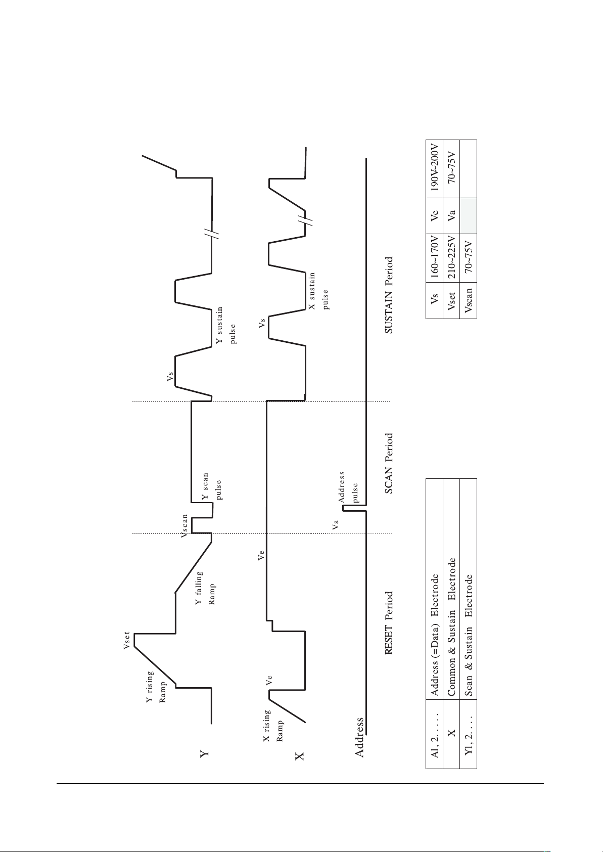
5-2-2 SPECIFICATION OF DRIVE PULSES
5-2-2(A) DRIVE PULSES
Page 32

Circuit Operation Description
Samsung Electronics 5-11
5-2-2(B) FUNCTIONS OF PULSES
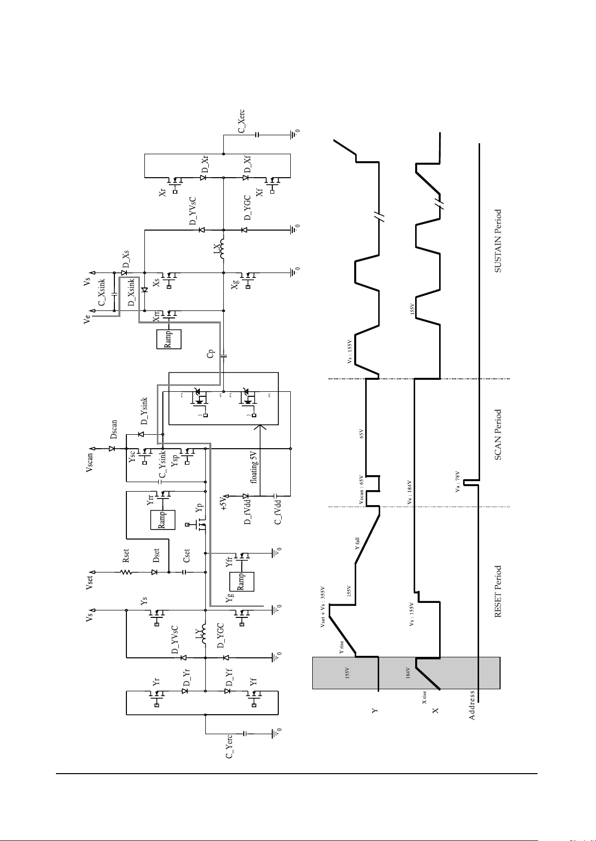
(1) X rising ramp pulse
Just before X rising ramp pulse is impressed, the last Y electrode sustain pulse of previous sub field is
impressed. The pulse causes sustain discharge. Consequently, positive wall charge is accumulated in X
electrode, and negative wall charge is accumulated in Y electrode. X rising ramp erases wall charge
produced by the last sustain discharge pulse using weak-discharge.
(2) Y rising ramp pulse
During Y rising ramp period, weak-discharge begins when external voltage of about 390V~400V is
impressed to Y electrode, and each gap voltage is equal to discharge start voltage. Sustaining the
weak-discharge, positive wall charge is accumulated in X electrode and address electrode, and negative wall charge is accumulated in Y electrode of the entire panel.
(3) Y falling ramp pulse
During Y falling ramp period, the negative wall charge in Y electrode accumulated by 200V of X bias
is used to erase positive wall charge in X electrode. Address electrode (0V) sustains most of the positive electric charge accumulated during rising ramp period so that it can maintain wall charge distribution beneficial to the upcoming address discharge.
(4) Y scan pulse
This is called the scan pulse, selecting each of Y electrodes on a one-line-at-a-time basis. In this case,
Vscan means the scan bias voltage. About 70 V (Vscan) voltage is impressed on the selected electrode
lines, while 0 V (GND) voltage is impressed on the other lines.
In the cells the address pulse (70V~75V) is impressed on, address discharge is occurred because negative wall charge is accumulated in Y electrode, positive wall charge is accumulated in address electrode by the applied ramp pulse, and the sum of impressed voltage is greater than discharge start
voltage. Thus, because scan pulse and data pulse are impressed line by line, very long time is taken
for PDP addressing.
(5) 1st sustain pulse
The sustaining pulse always begins with the Y electrode. This is because when address discharge is
generated, positive wall voltage is generated on the Y electrodes. Because wall electric charge generated by address discharge is generally smaller than wall voltage generated by sustaining discharge, initial discharges have small discharge strength, and stabilization is usually obtained after 5~6 times discharges, subject to variations depending on the structure and environment of electrodes. The purpose
of impressing the initial sustaining pulses long is to obtain stable initial discharges and generate wall
electric charges as much as possible.
Page 33
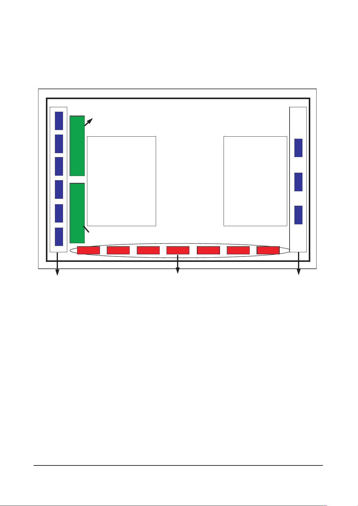
5-2-3(A) FUNCTIONS OF EACH BOARD
(1) X board
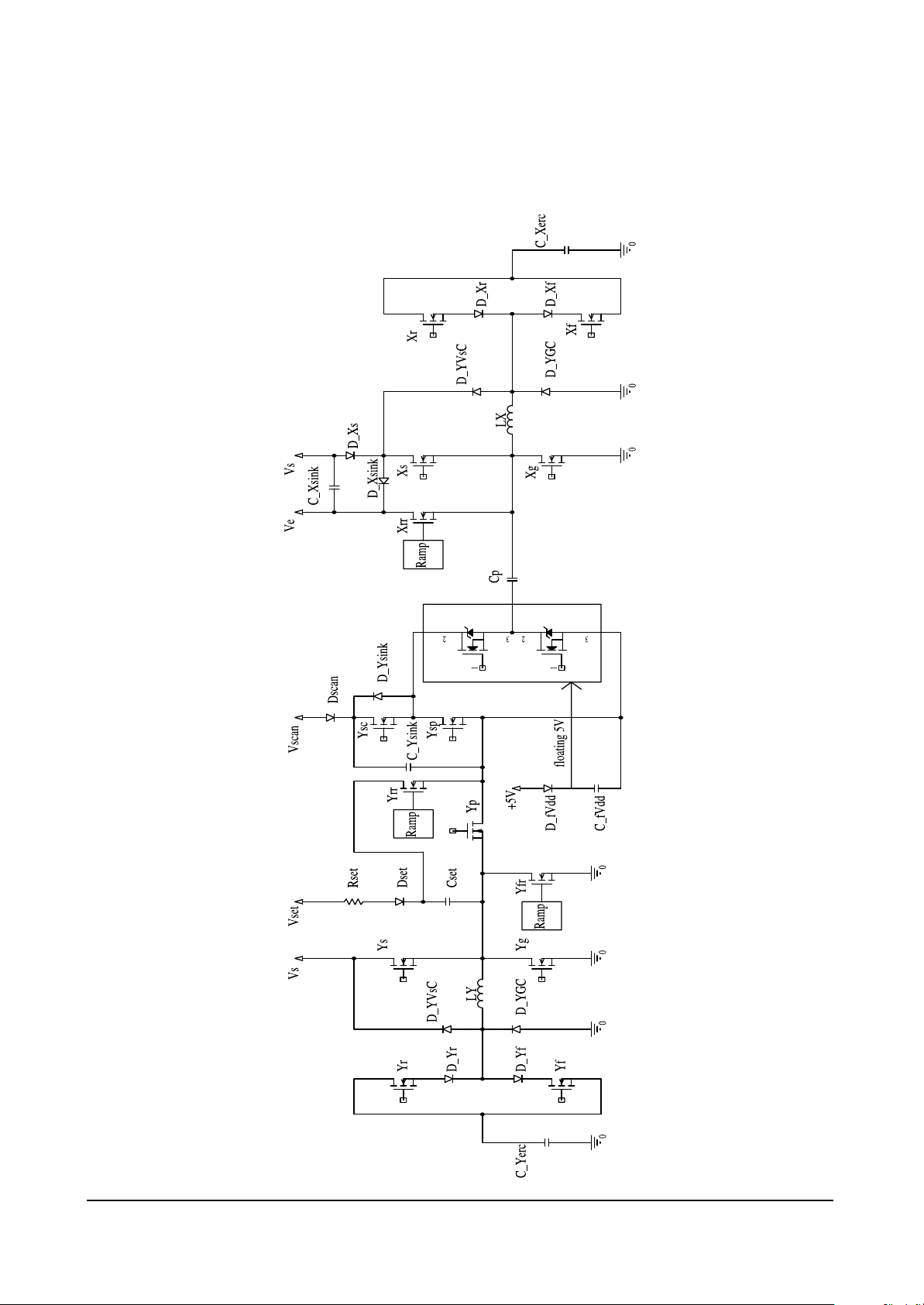
X board is connected to the panel’s X-electrode blocks, 1) generates sustain voltage pulse (including
ERC), 2) generates X rising ramp pulse, and 3) sustains Ve bias during scan period.
(2) Y board
Y board is connected to the Y-electrode blocks of panel, 1) generates sustain voltage pulse (including
ERC), 2) generates Y rising and falling ramp pulse, and 3) sustains Vscan bias.
(3) Y buffer board (upper and lower)
Y buffer board impresses scan pulse to Y electrodes, and consists of upper and lower sub-boards. In
case of SD class, one board is equipped with 4 scan driver IC’s (STMicroelectronics STV7617 with 64
or 65 outputs).
(4) COF
Impresses Va pulse on address electrodes in the address section and generates address discharge
based on a difference between such Va pulse and scan pulse impressed on Y electrodes. It is in the
form of COF, and a COF is equipped with 4 data drive IC’s (STMicroelectronics STV7610A with 96
outputs). For a single scan, 7 COF’s are required.
Circuit Operation Description
5-12 Samsung Electronics
5-2-3 Configuration and Operation Principles of Driver Circuit
Y-Buffer (Upper)
Y Drive board
- Sustain pulse
(Energy recovery)
- Rising ramp pulse
- Falling ramp pulse
X Drive board
- Sustain pulse
(Energy recovery)
- Rising ramp pulse
- Ve bias
- Vscan pulse
Y-Buffer (Lower)
Y-electrode blocks
COF X-electrode blocks
(6 blocks)
(3 blocks)
Page 34
Circuit Operation Description
Samsung Electronics 5-13
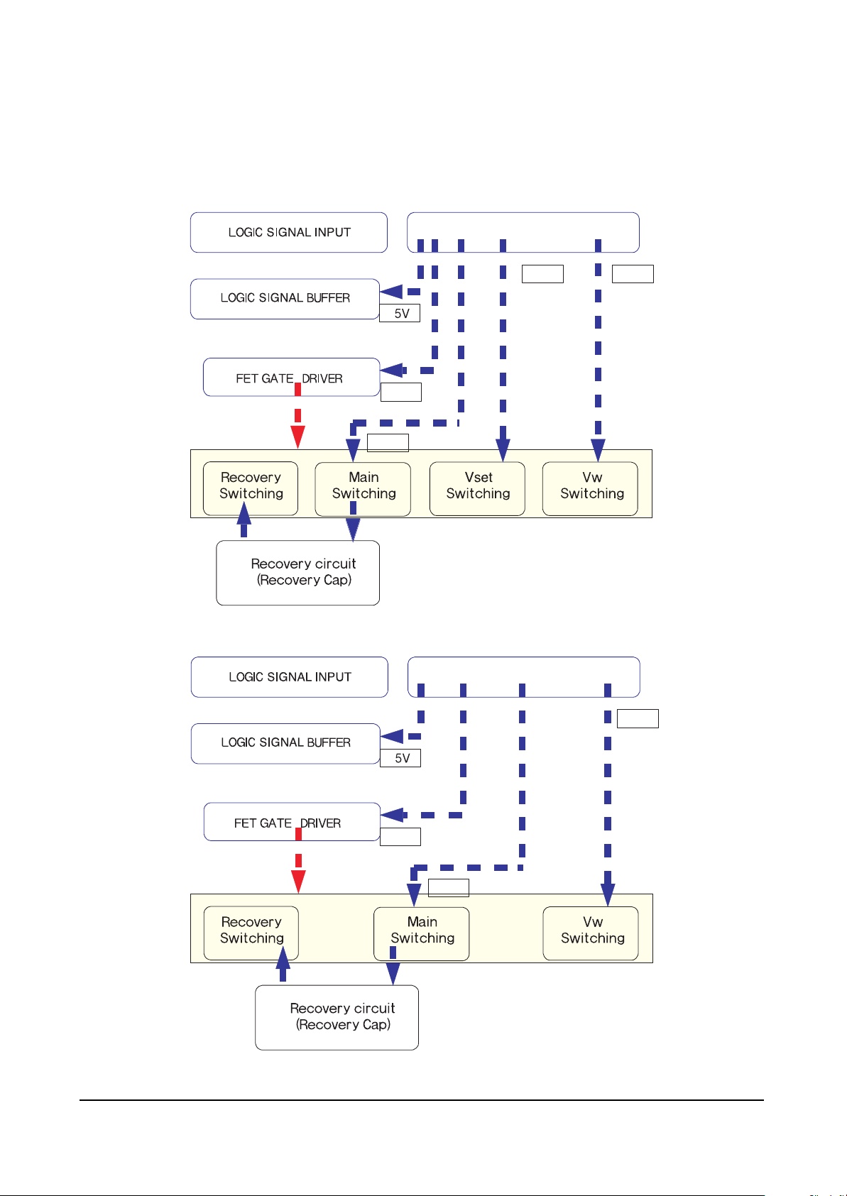
5-2-3(B) DRIVING BOARD'S BLOCK DIAGRAM
(1) Y
(2) X
17V
170V
POWER
220V
75V
POWER
220V
17V
170V
Page 35

Circuit Operation Description
5-14 Samsung Electronics
➣ Components of driving board's operations
1. Power supply
1) Supplied from the power supply board
- For sustaining discharge: 180V;
- For logic signaling buffer: 5V; and
- For gate driver IC: 15V.
2) Generated by the internal DC/DC part
- For generating Vw pulse: 180V.
2. Logic signal
1) Supplied from the logic board
- Gate signals for FETs.
Page 36
Circuit Operation Description
Samsung Electronics 5-15
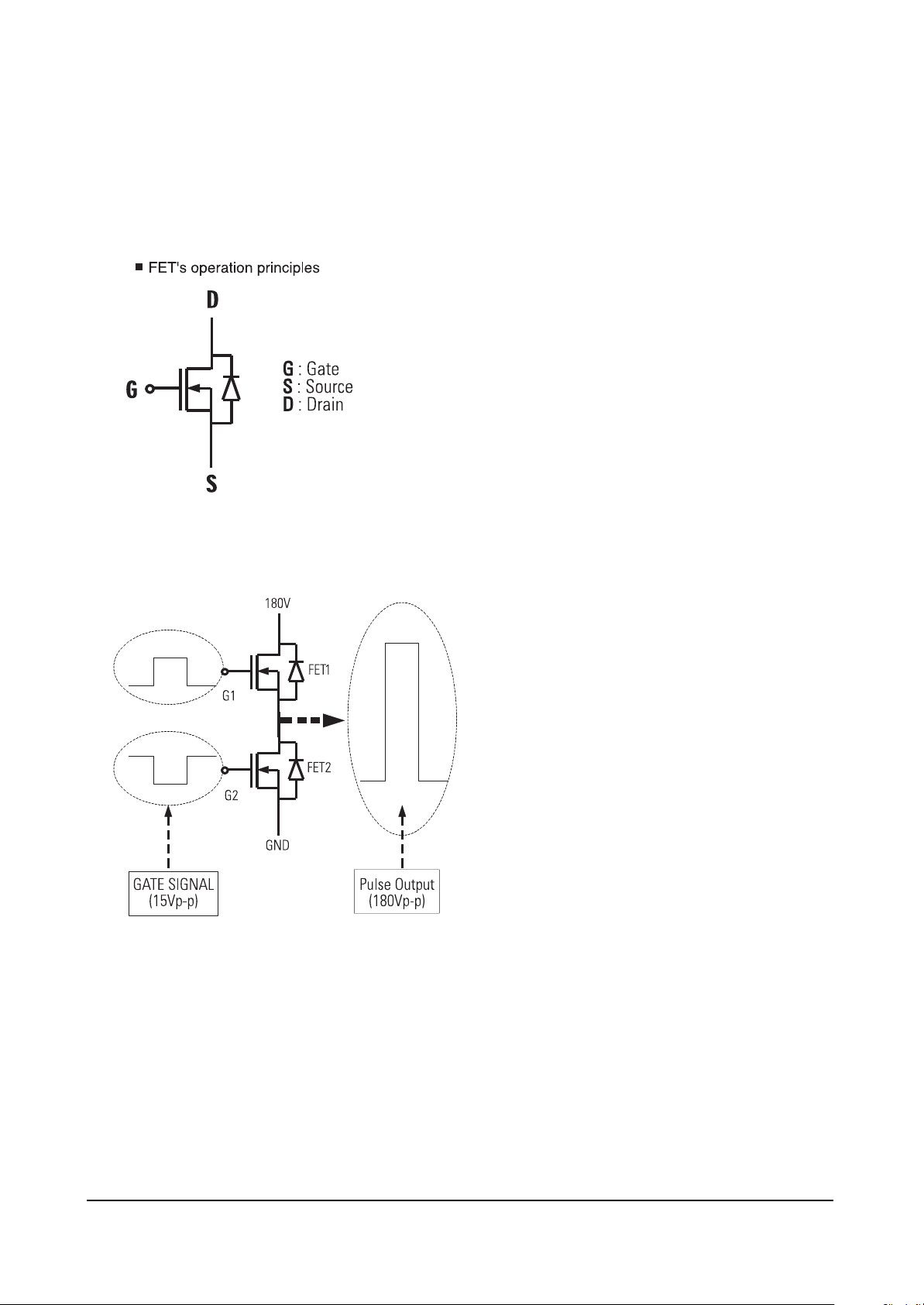
5-2-3(C) PRINCIPLES OF FET’S OPERATION AND HIGH VOLTAGE SWITCHIng
❏ FET’s operation principles
❏ FET’s high voltage switching principles
(1) With no signal impressed on G1, FET1 gets
open-circuited, and with signal impressed on
G2, FET2 gets short-circuited, thereby causing
GND to be outputted to output terminals.
(2) With signal impressed on G1, FET1 gets short-
circuited, and with no signal impressed on G2,
FET2 gets open-circuited, thereby causing
180V to be outputted to output terminals.
(1) With signal impressed on the gate (Positive voltage),
FET gets short-circuited (a conducting wire of zero (0)
resistance); and
(2) With no signal impressed on the gate (GND), FET gets
open-circuited (a non-conducting wire of ∞ resistance).
Page 37
Circuit Operation Description
5-16 Samsung Electronics
5-2-3 (D) DRIVER CIRCUIT DIAGRAM
Page 38
Circuit Operation Description
Samsung Electronics 5-17
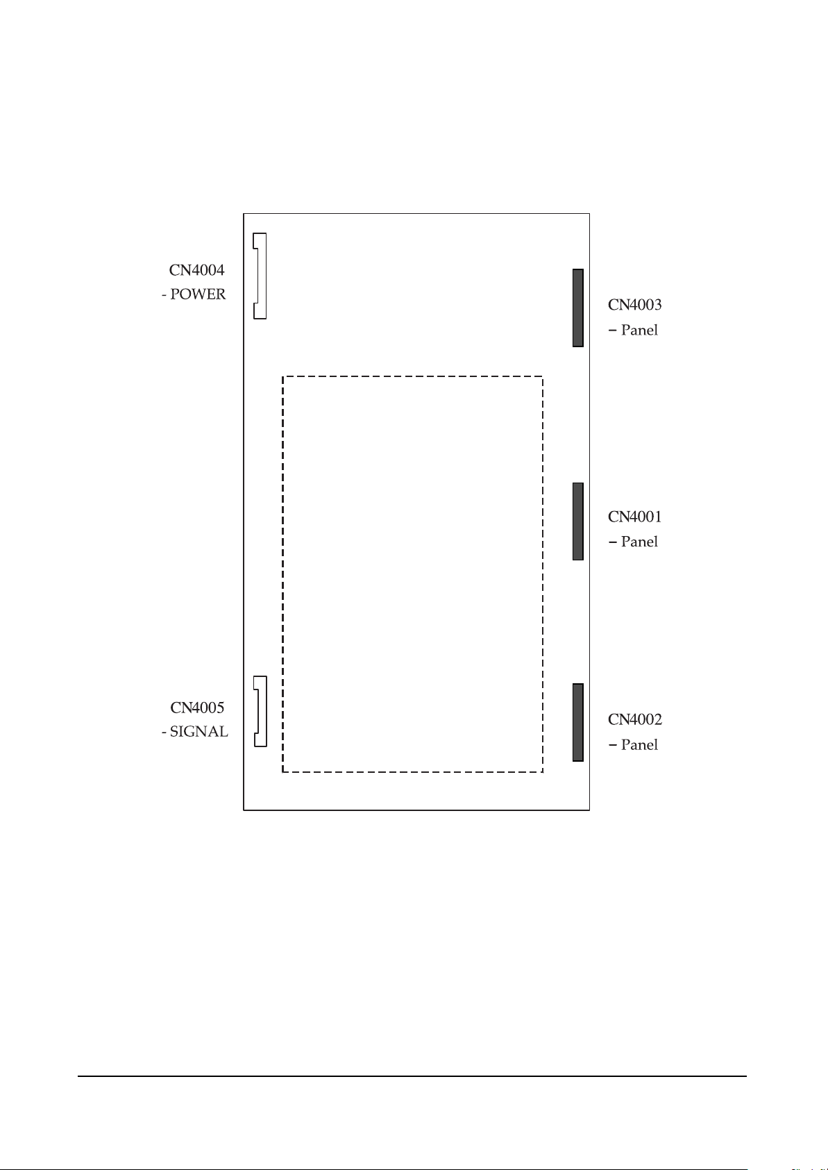
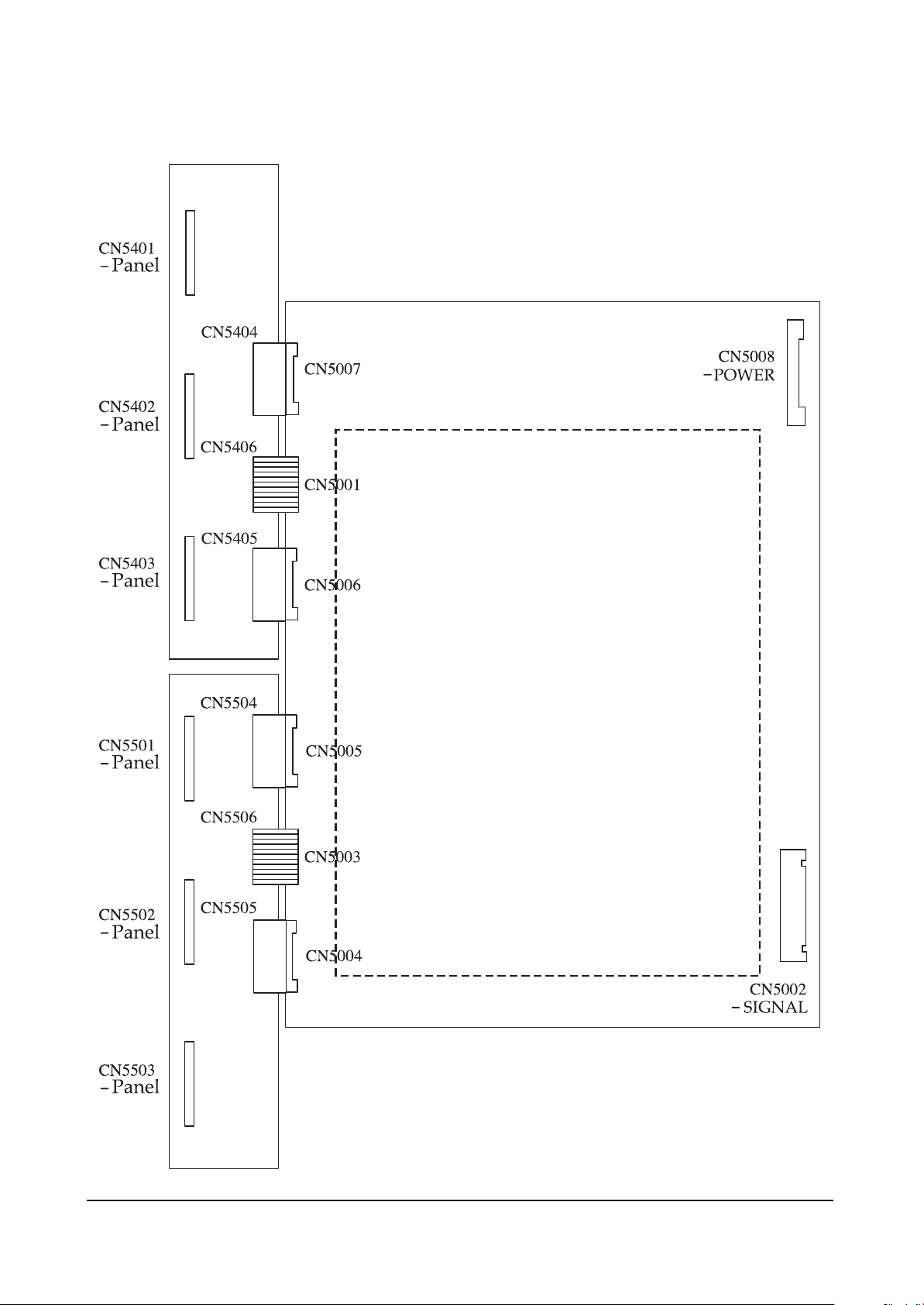
5-2-3(E) DRIVER BOARD CONNECTOR LAYOUT
Page 39
Circuit Operation Description
5-18 Samsung Electronics
Page 40
Circuit Operation Description
Samsung Electronics 5-19
Page 41
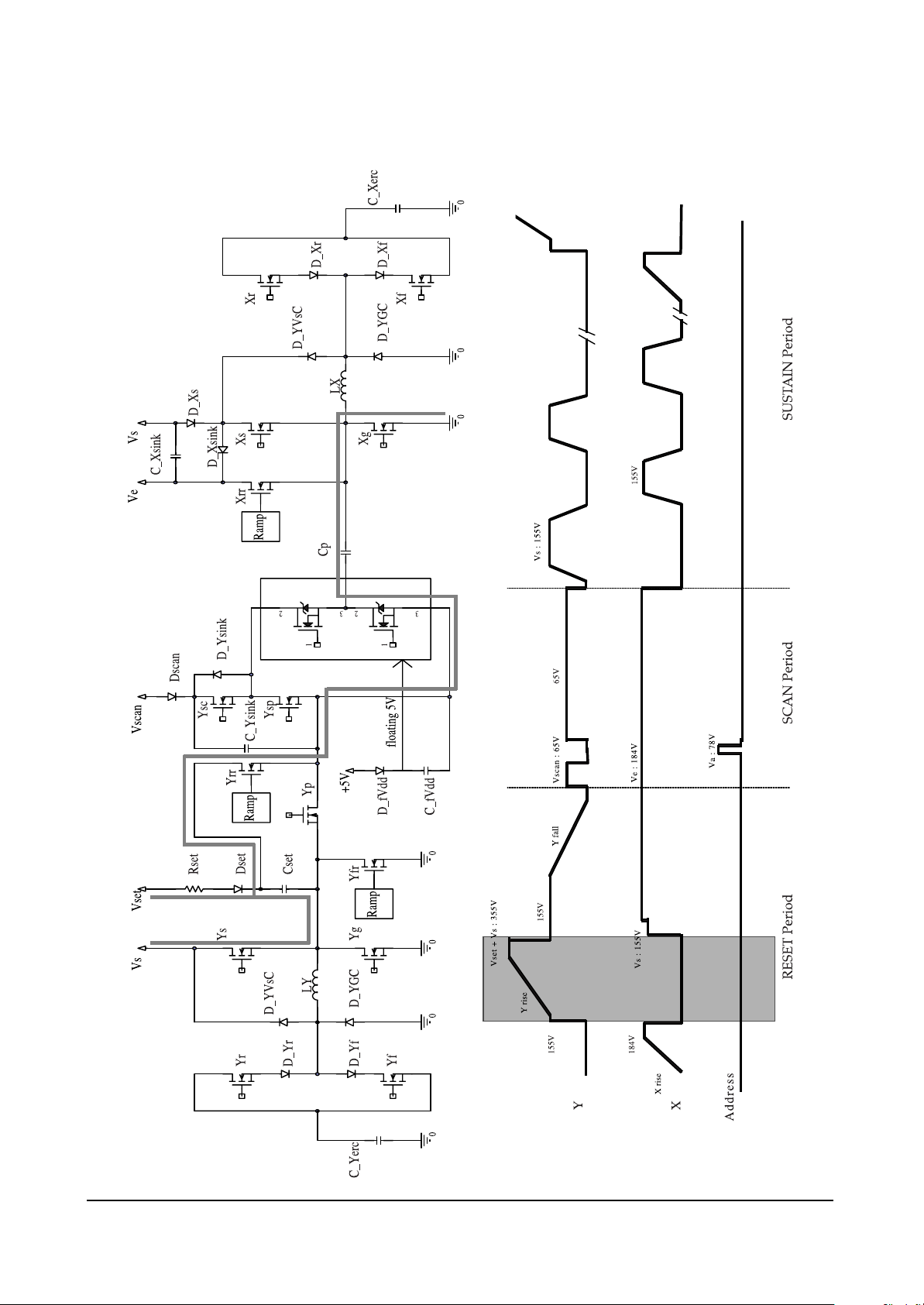
Circuit Operation Description
5-20 Samsung Electronics
Page 42
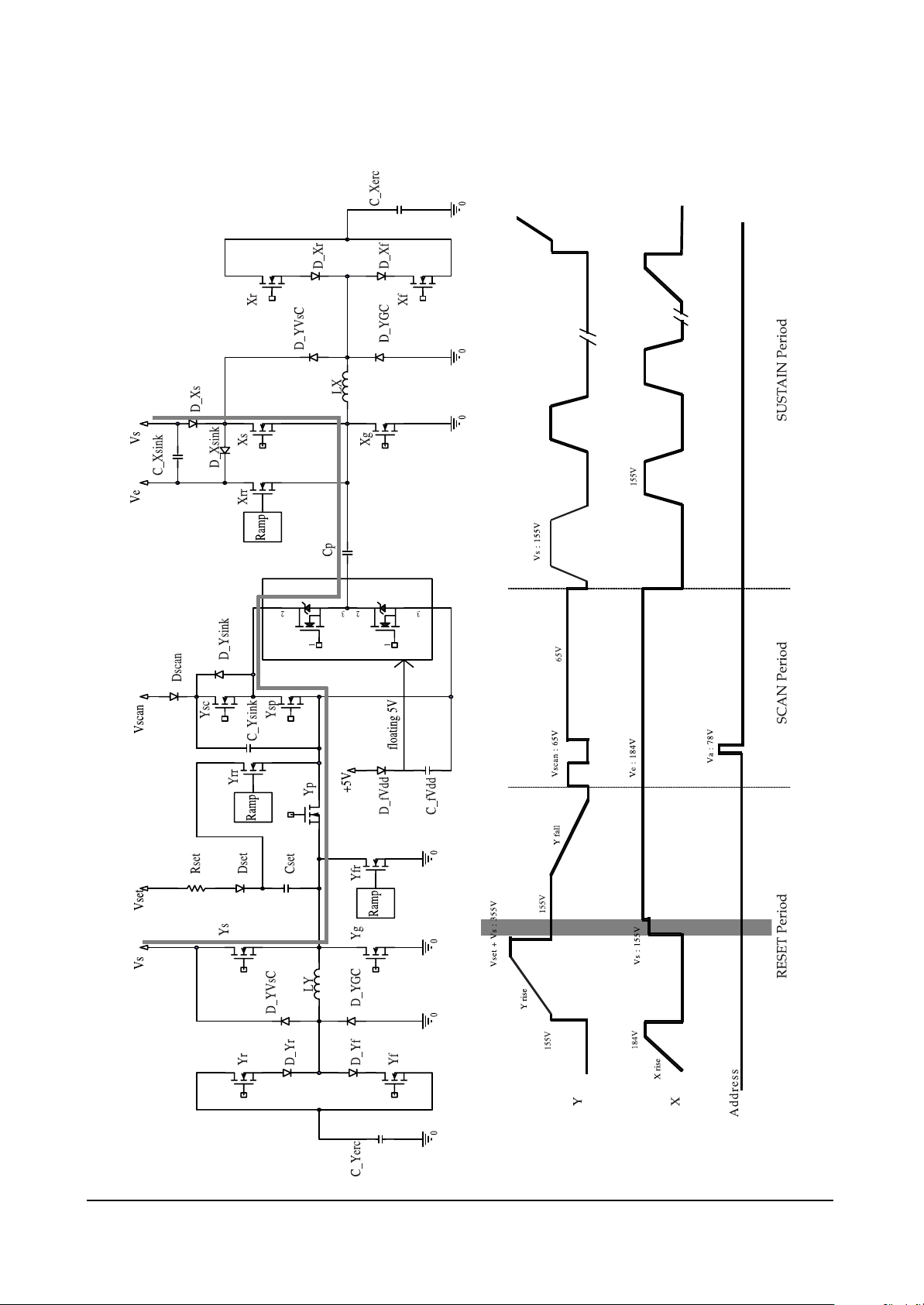
Circuit Operation Description
Samsung Electronics 5-21
Page 43
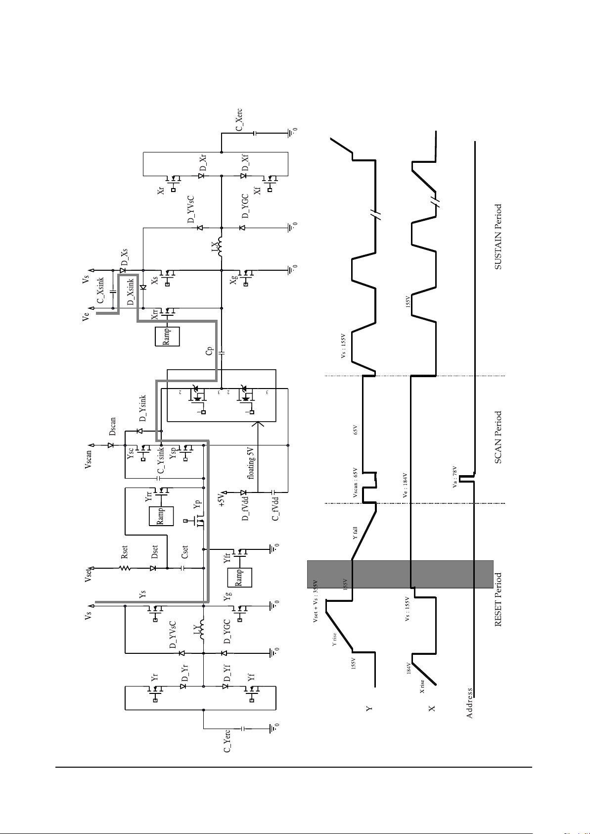
Circuit Operation Description
5-22 Samsung Electronics
Page 44
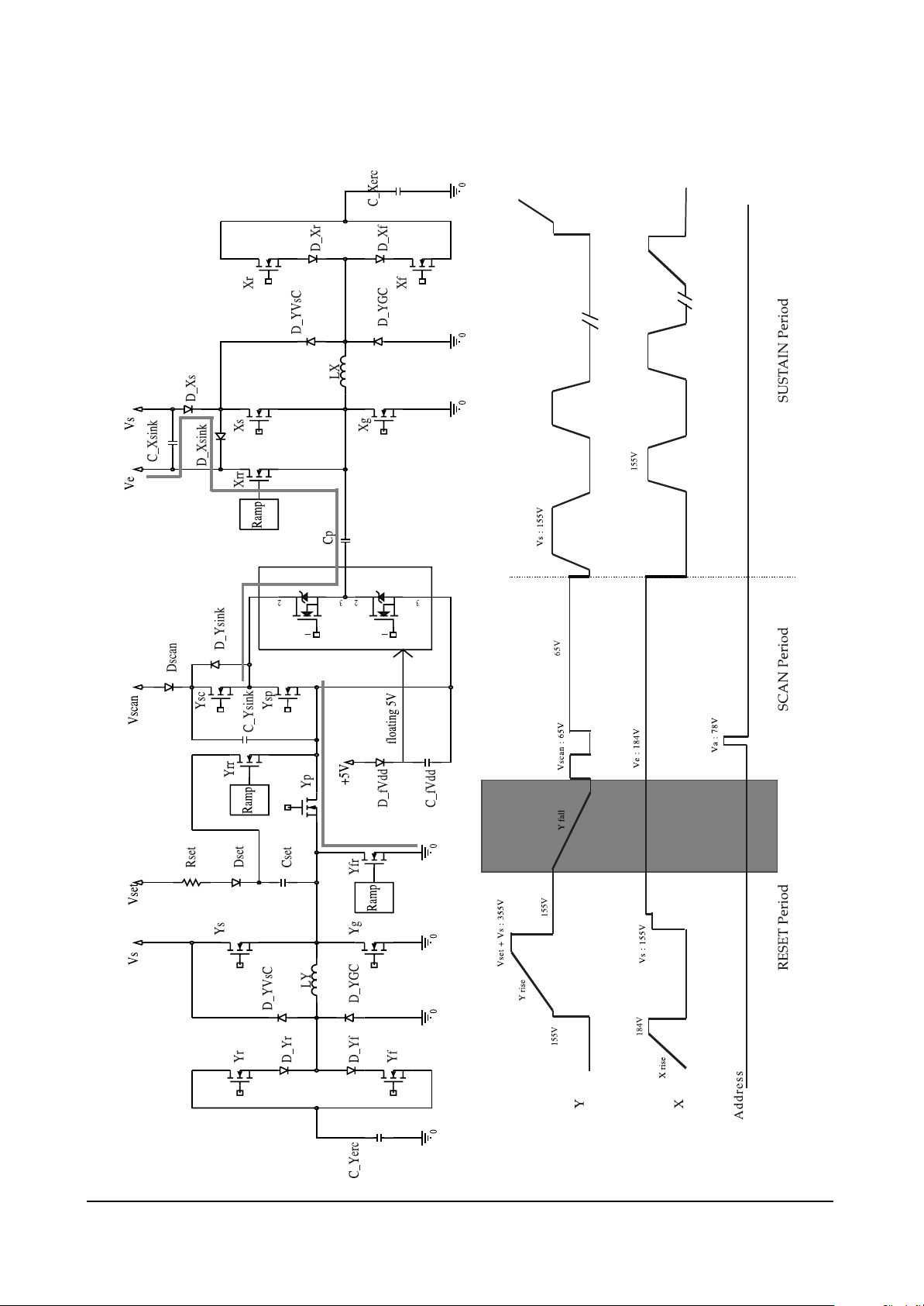
Circuit Operation Description
Samsung Electronics 5-23
Page 45
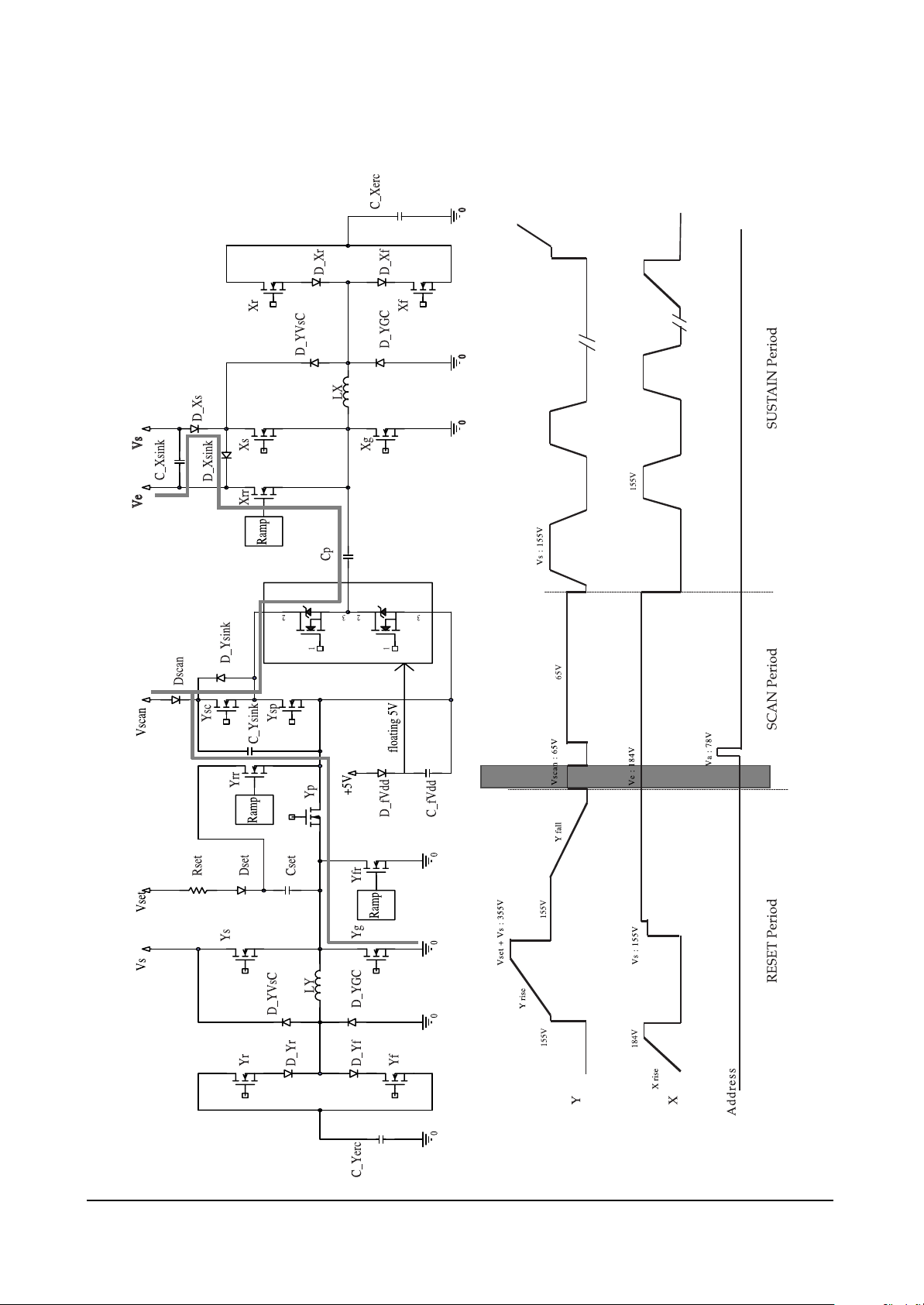
Circuit Operation Description
5-24 Samsung Electronics
Page 46
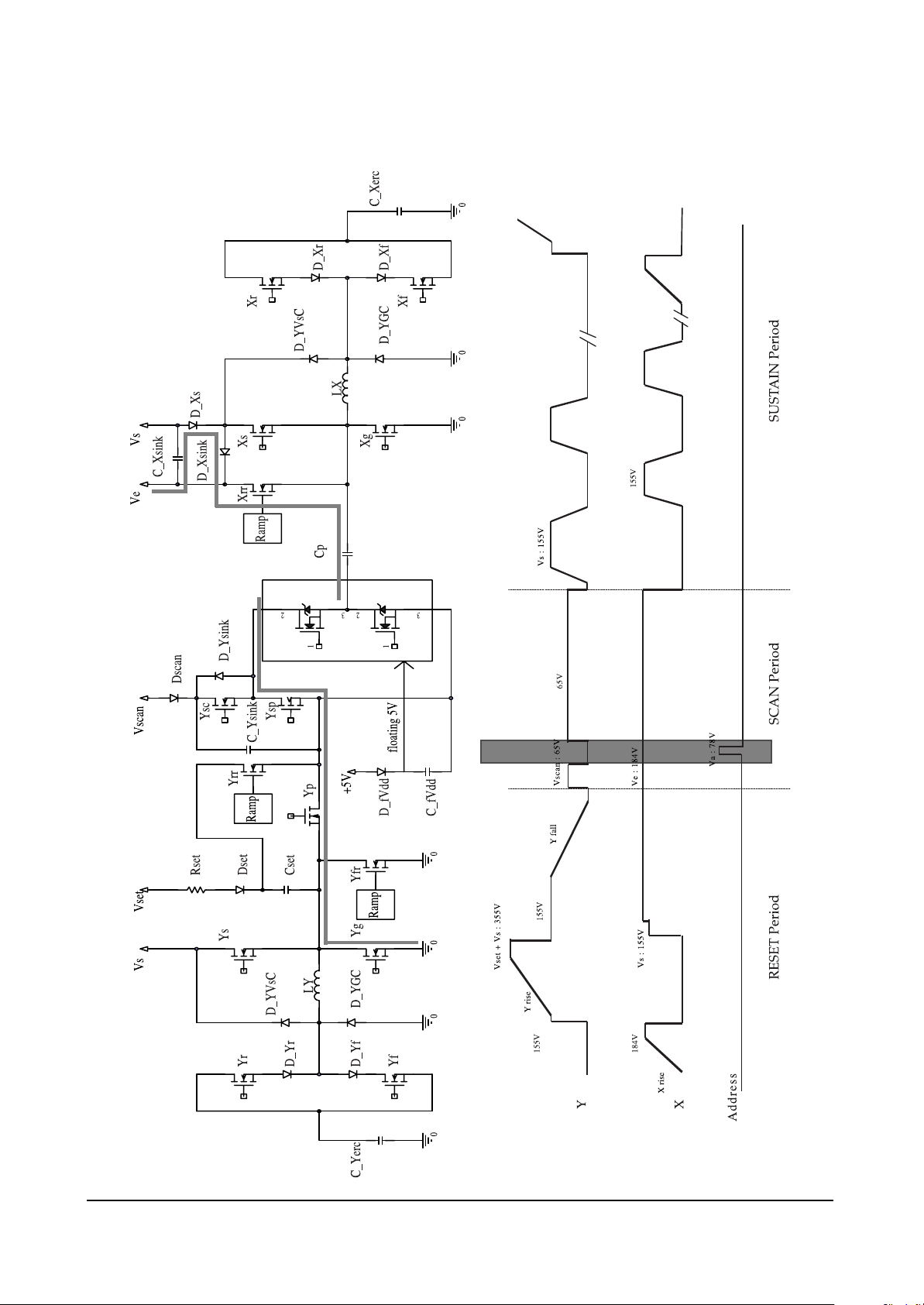
Circuit Operation Description
Samsung Electronics 5-25
Page 47
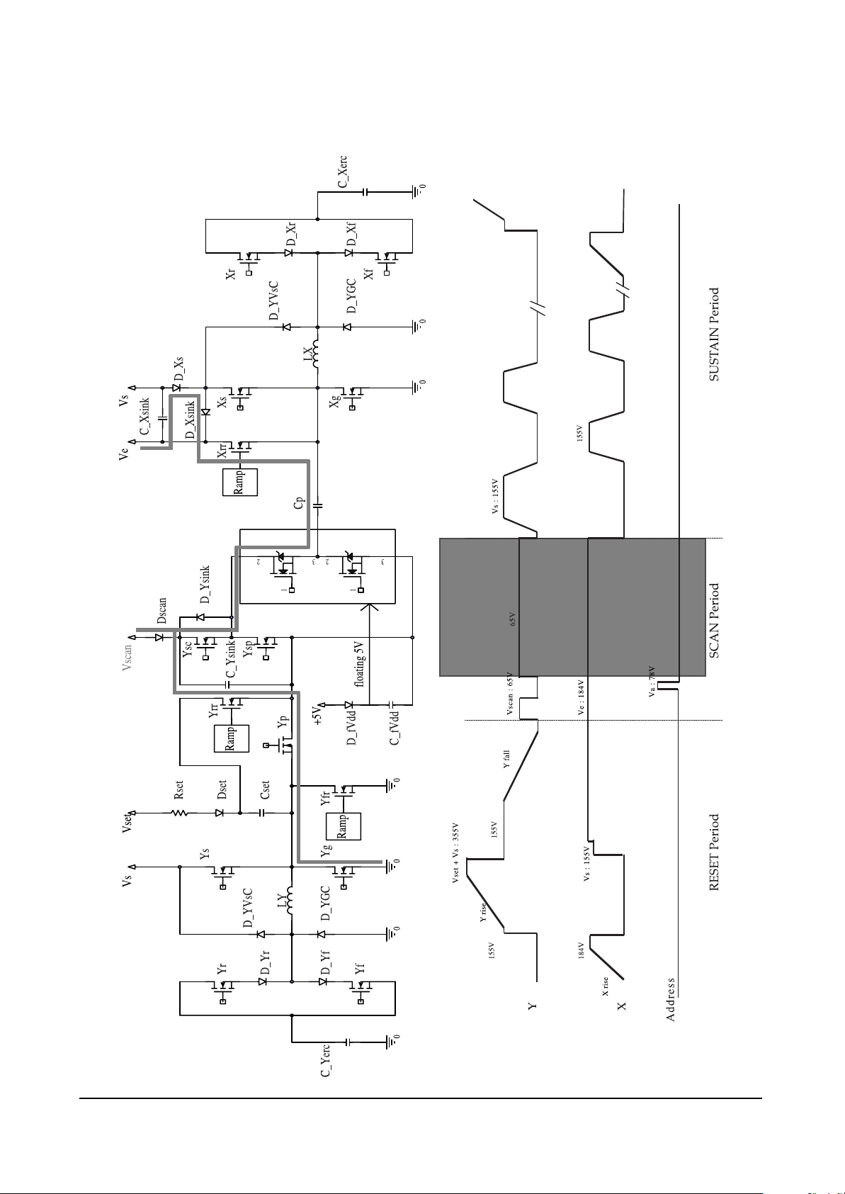
Circuit Operation Description
5-26 Samsung Electronics
Page 48
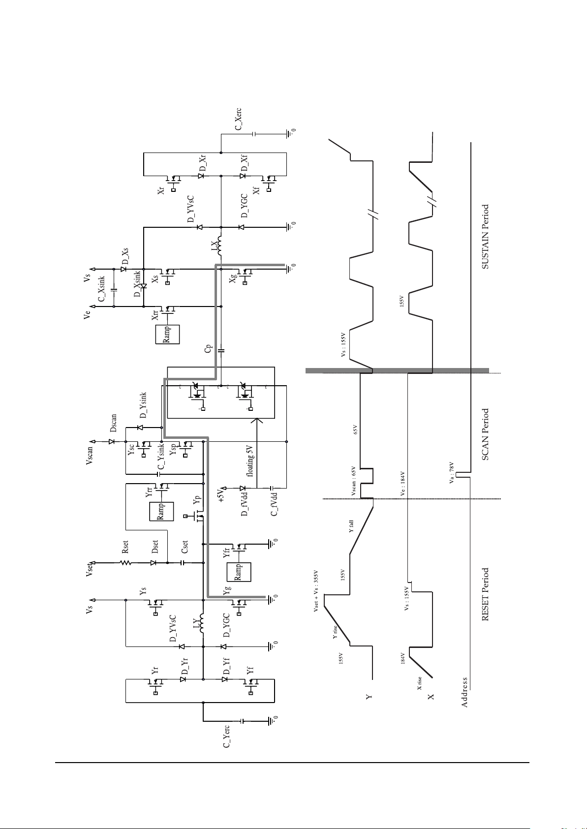
Circuit Operation Description
Samsung Electronics 5-27
Page 49
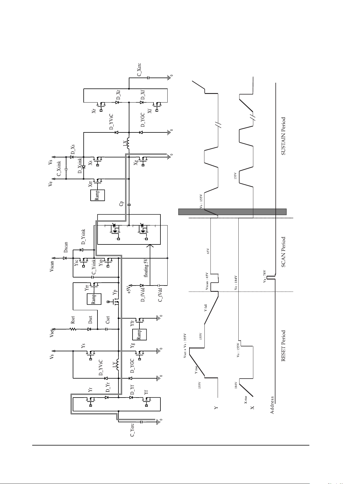
Circuit Operation Description
5-28 Samsung Electronics
Page 50
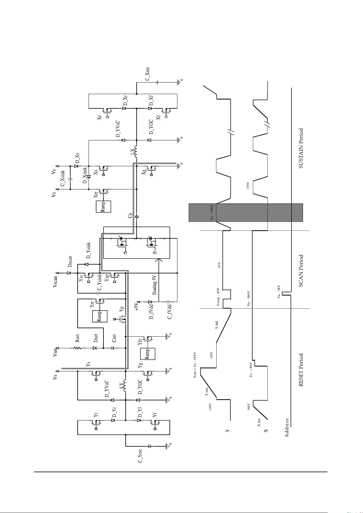
Circuit Operation Description
Samsung Electronics 5-29
Page 51
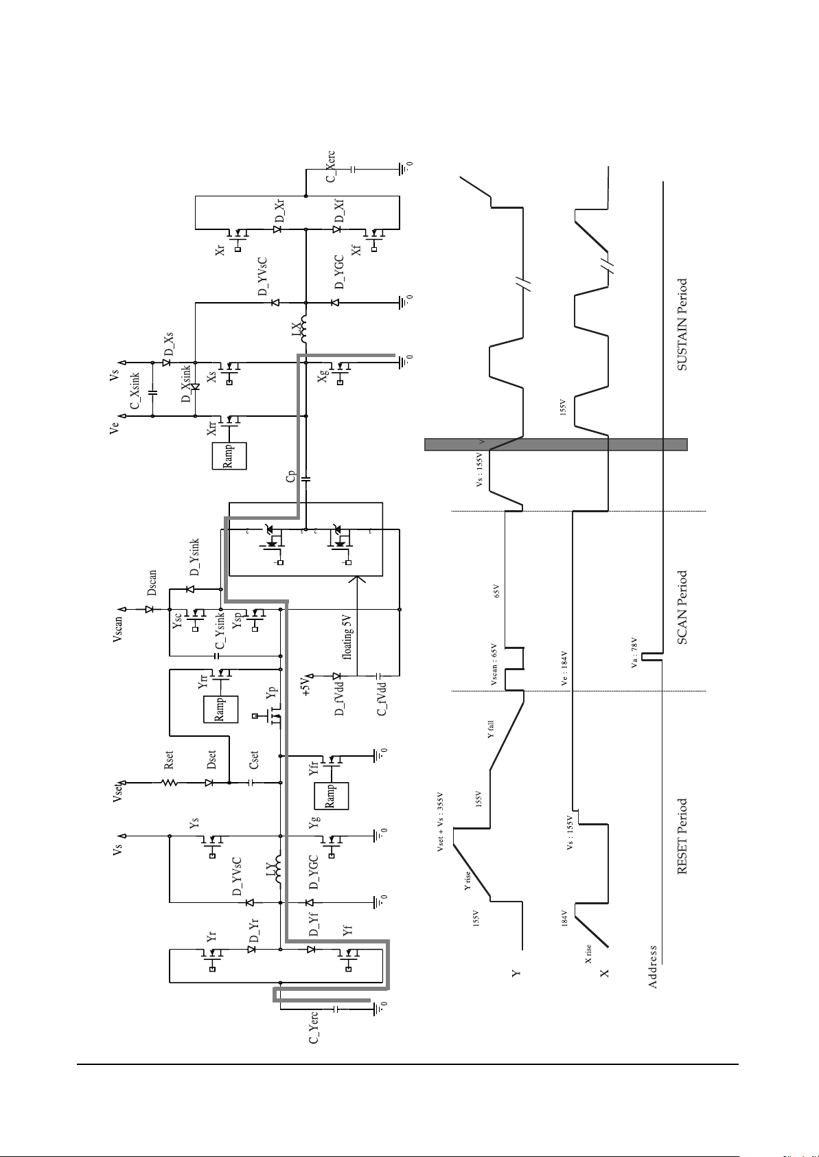
Circuit Operation Description
5-30 Samsung Electronics
Page 52
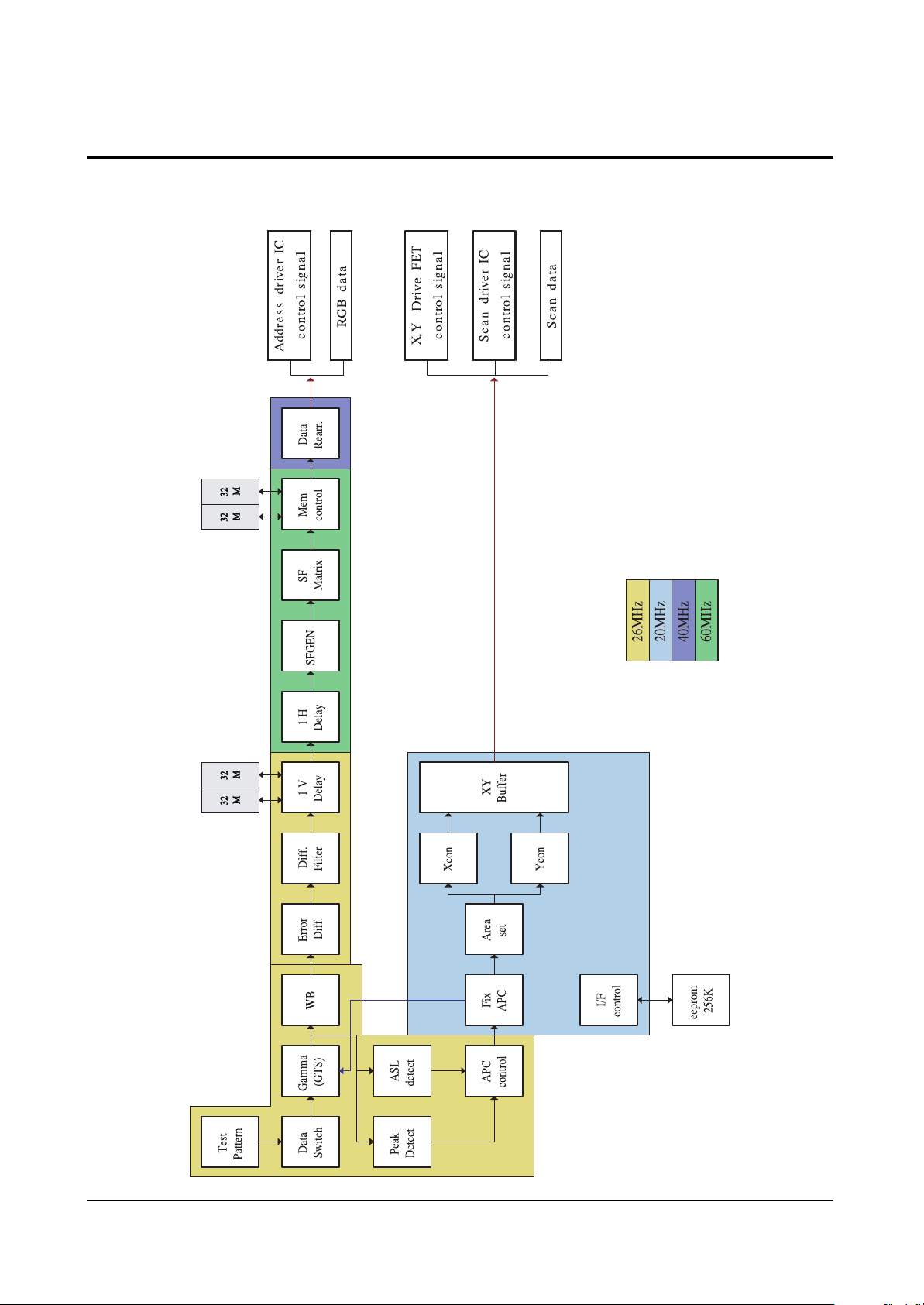
Circuit Operation Description
Samsung Electronics 5-31
5-3 Logic part
5-3-1 Logic Board Block diagram
Page 53
Circuit Operation Description
5-32 Samsung Electronics
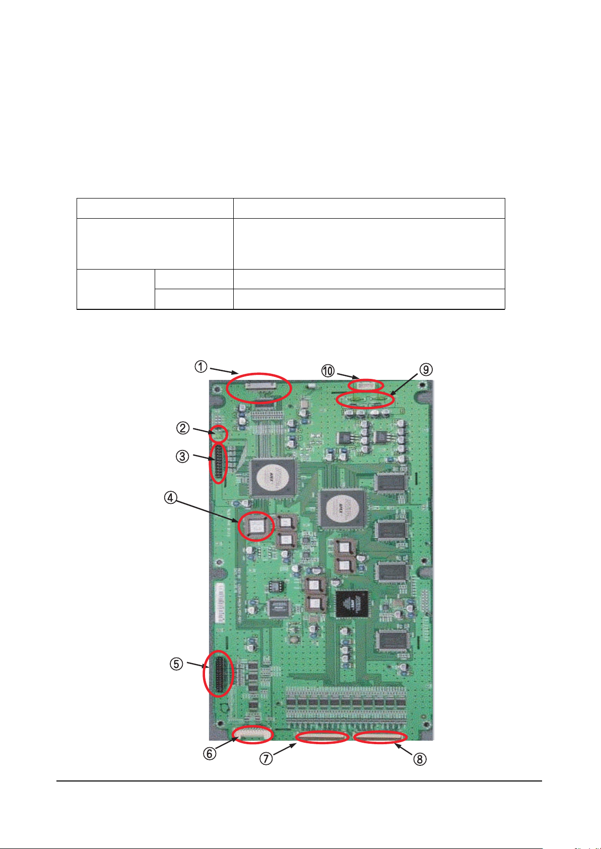
5-3-1(A) TDESCRIPTION OF LOGIC BOARD
The logic board consists of the logic main board and the buffer board. The logic main board processes video
signal, generates, and output address driver output signal as well as XY drive signal. The buffer board
stores address driver output signal, and sends the signal to the address driver IC (COF module).
5-3-1 (B) NAME AND DESCRIPTION OF MAJOR COMPONENTS OF LOGIC BOARD
Logic Board
Login Main
Function
- Video signal processing (W/L, Error diffusion, APC)
- Outputs address drive control signal, and data signal to buffer board.
- Outputs XY drive board control signal.
Buffer board
E Buffer board
F Buffer board
Sends data and control signal to left-bottom COF
Sends data and control signal to right-bottom COF
Page 54
Circuit Operation Description
Samsung Electronics 5-33
5-3-1(C) WAVEFORMS IN NORMAL OPERATION
If the PDP unit and the logic board is in normal operation, the operation LED of Figure 1 would blink at
about 1 second interval.
If the unit is out of order, check the status of the operation LED through eye-inspection first. If the behavior
of the operation LED is different from that of normal state, you have to replace the board. To check trouble
on the board, the following logic board test procedures described below.
❑ 42°” SD s1.0 logic main board T/S
Required test equipment: : - Oscilloscope (digital 400 MHz 3 channel or more)
- Multi meter
Other equipment: : - DC power supply (5V: 1EA)
- Sub-PCB ASS'Y for JIG: 1 EA
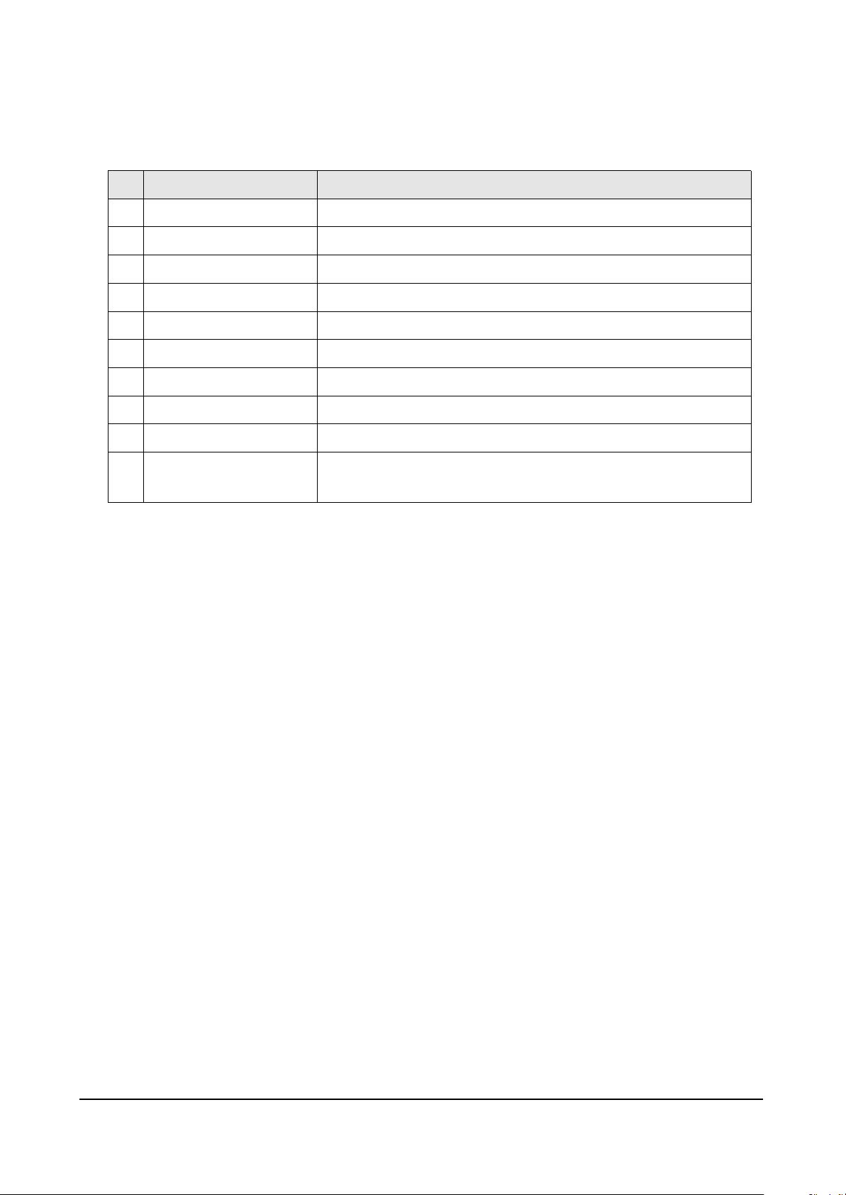
Name
LVDS Connector
Operation LED
Key-Scan Connector
256k
Y Connector
X Connector
LE01 (Address Buffer Connector)
LE02 (Address Buffer Connector)
Power Fuse
Power Connector
No
1
2
3
4
5
6
7
8
9
10
Function
Input connector to receive encoded RGB, H, V, DATAEN, and DCLK signal.
It shows Sync and clock are properly received by the logic board.
Connector to connect key scan board to check and adjust 256K data.
EEPROM including gamma table, APC table, drive signal timing and other options
Connector to output Y drive board control signal
Connector to output X drive board control signal
Connector to output address data, and control signal to the E and F buffer boards.
Connector to output address data, and control signal to the E and F buffer boards.
Fuse connected to the power source line of the logic board.
Connector to connect the supply power (5V) with the logic board.
drive board control signal.
Page 55
Circuit Operation Description
5-34 Samsung Electronics
(1) First, perform eye-inspection and short circuit inspection for the power stage of the logic board to exam-
ine. Then, perform the following examinations on the board in order if no problem was found.
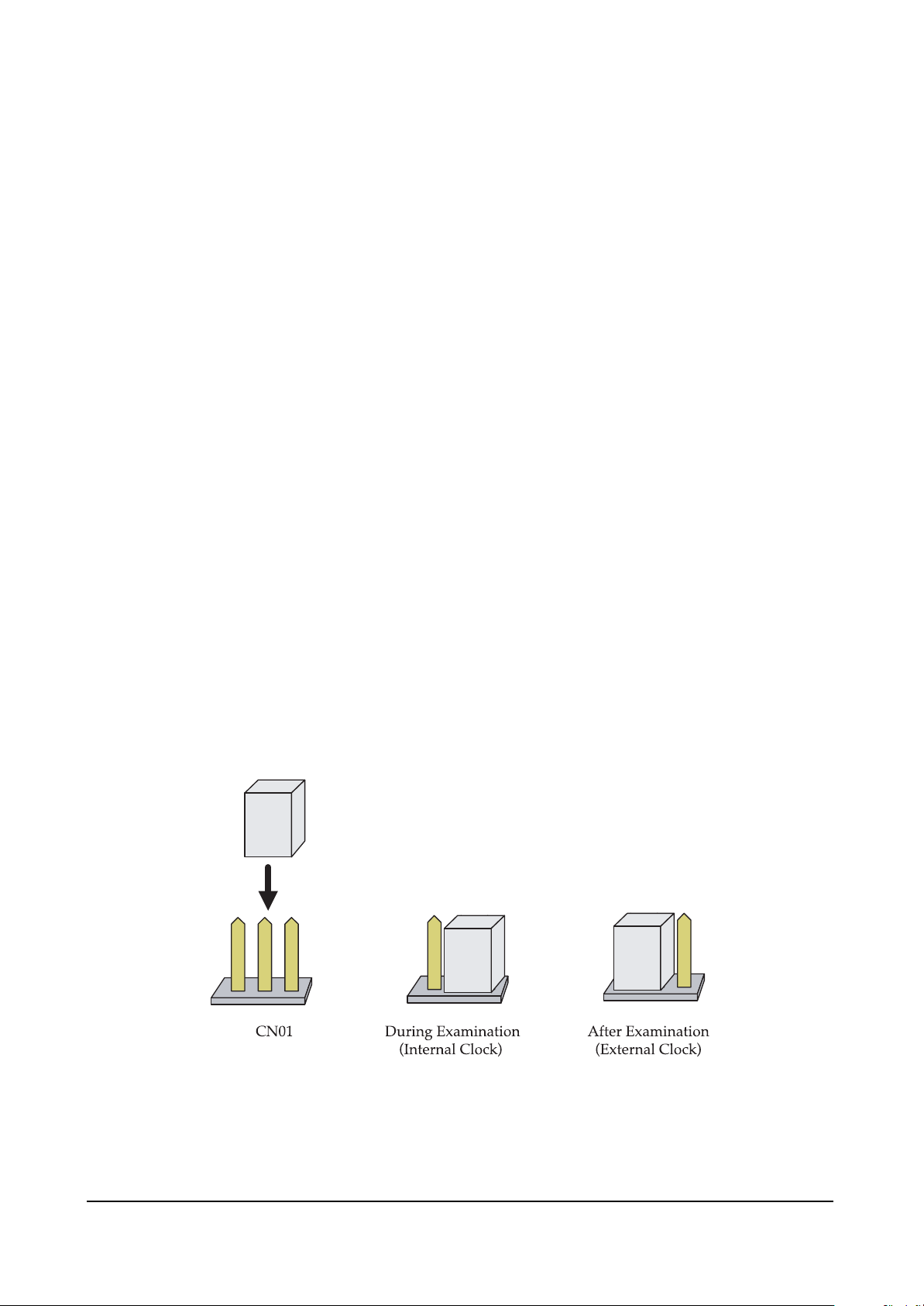
(2) Replace IC2017(256K EEPROM) of the logic board with Test EERPOM. Change the clock setting of the
logic board to internal referring to the configuration procedures described below.
❈ If there is no available Test EEPROM, you can use PG 00 for Windows NT systems, or PG 40 for
NT/PAL compatible systems by setting address 20 to 81, 22 to 00, 23 to 00,and 70 to 01.
(3) Connect power(5V) to LD1, and check that LED(LD2000) on the left top of the board blinks at about 1
second interval.
(4) If the logic board is out of order, the LED would blink too fast or not be lighted on.
(5) If no problem was found in the above examination, connect sub-PCB for logic output examination, mea-
sure output waveform, and compare the waveform with the appended waveform of normal state.
Record either OK or NG after examination.
(6) Check drive Y s/w, drive X s/w and address signal in order.
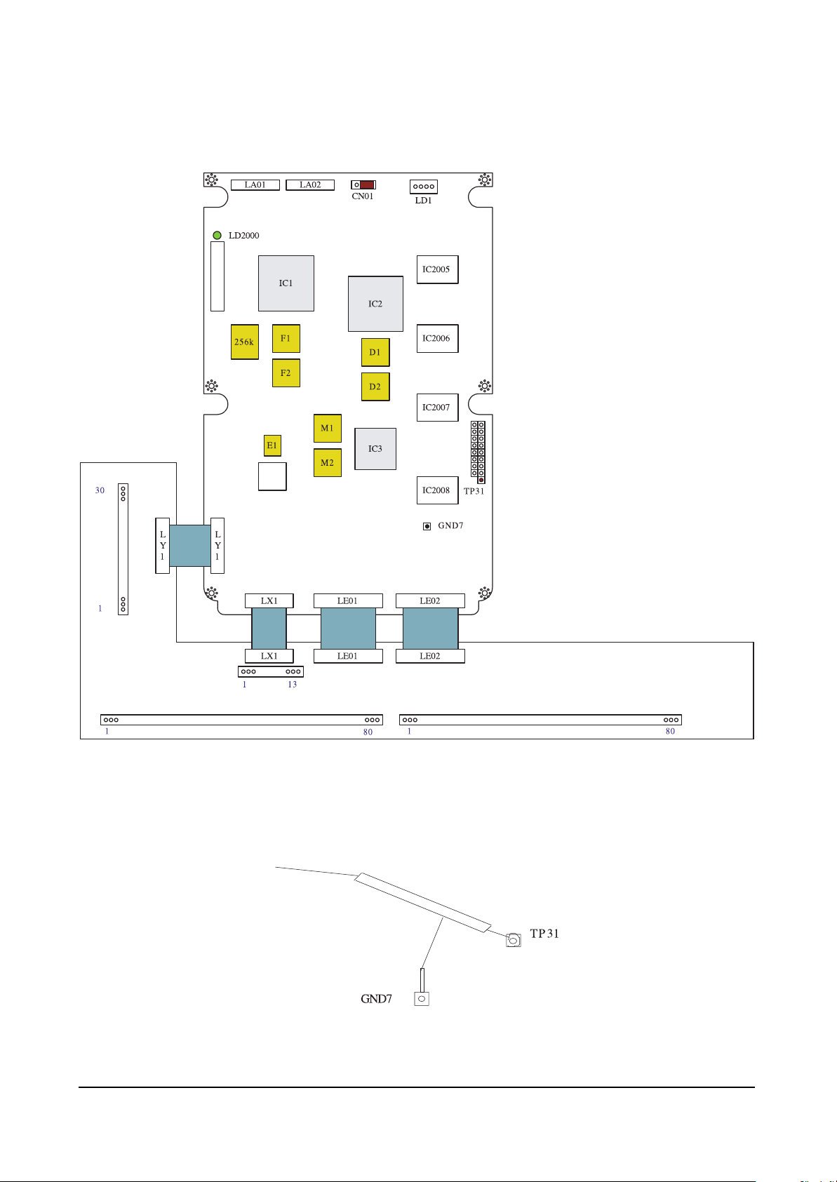
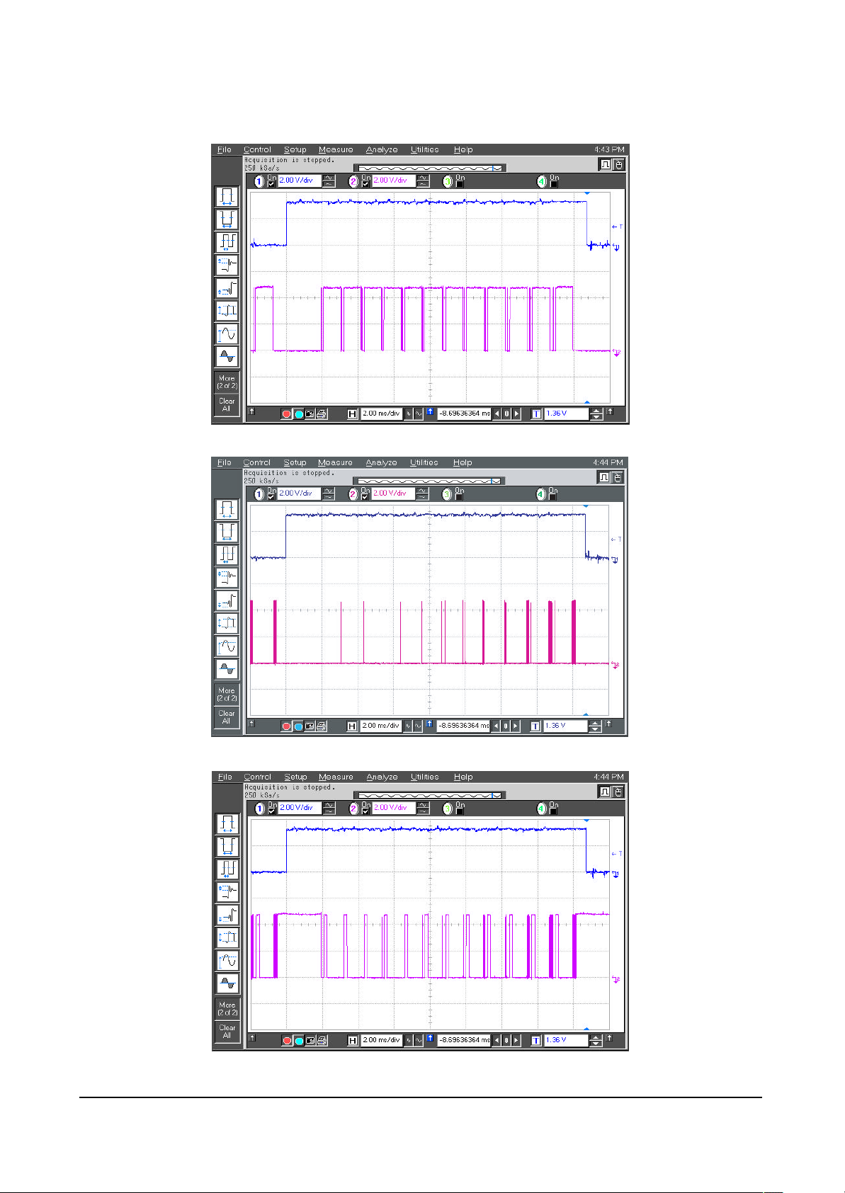
(7) Set probe 1 of oscilloscope to trigger signal, and connect it to the TP31 of the logic board.
(8) Set oscilloscope to 2ms/div. After adjusting probe 2 to 5V/div, check output signal.
(9) After T/S, turn off the power supply, and disconnect connector.
(10) Record the result on the examination sheet (either OK or NG).
❐ Jumper settings to select internal or external clock
On the top of the logic main board, there is option jumper (CN01) that allows selecting internal/external
clock. While T/S, set it to internal clock as the following figure shows.
❈ It is set to external clock in normal. Set it to internal clock while examination, and set it to external
clock again after examination.
Figure 1. Jumper Settings to Select Internal / External Clock Signal
Page 56
Circuit Operation Description
Samsung Electronics 5-35
LA03
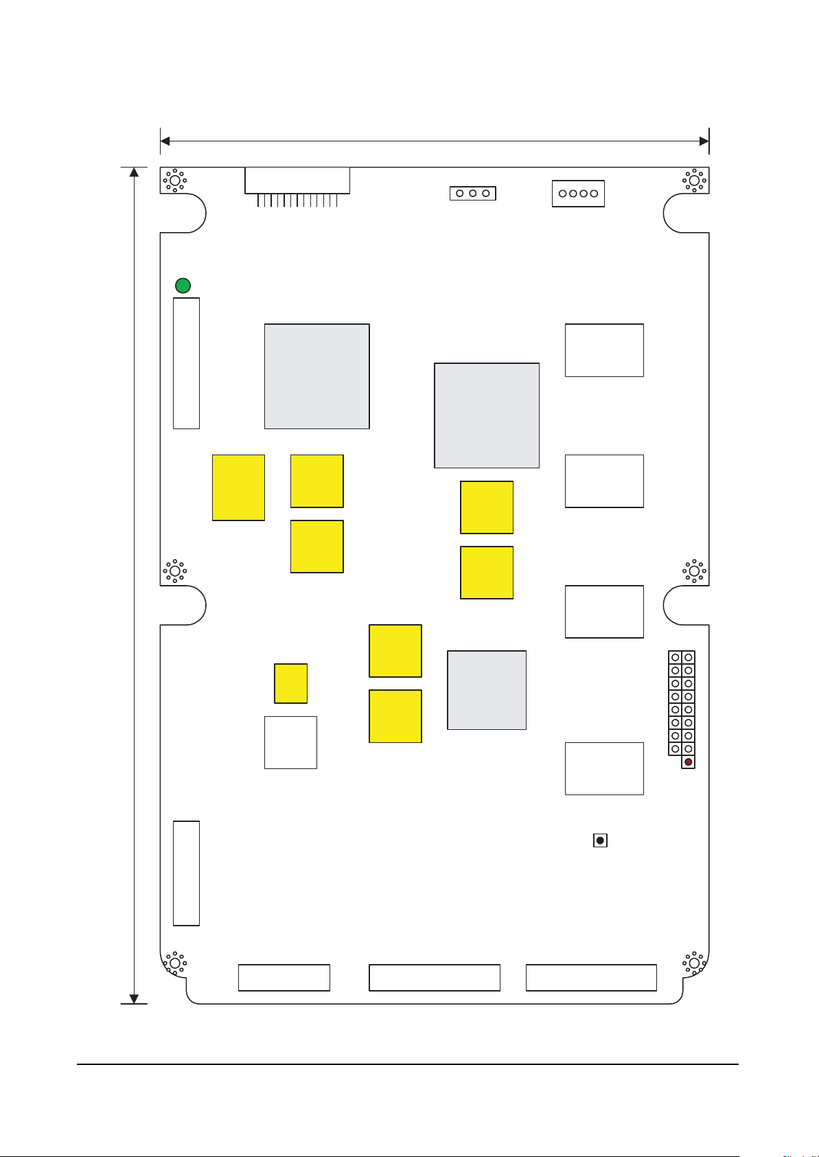
Figure 2. Layout of 42" Signal Logic Main Board.
160mm
320mm
LD2000
256k
IC1
F1
F2
131
CN01
LD1
IC2
D1
D2
L
Y
1
M1
E1
IC3
M2
LX1 LE01 LE02
TP31
GND7
Page 57
Circuit Operation Description
5-36 Samsung Electronics
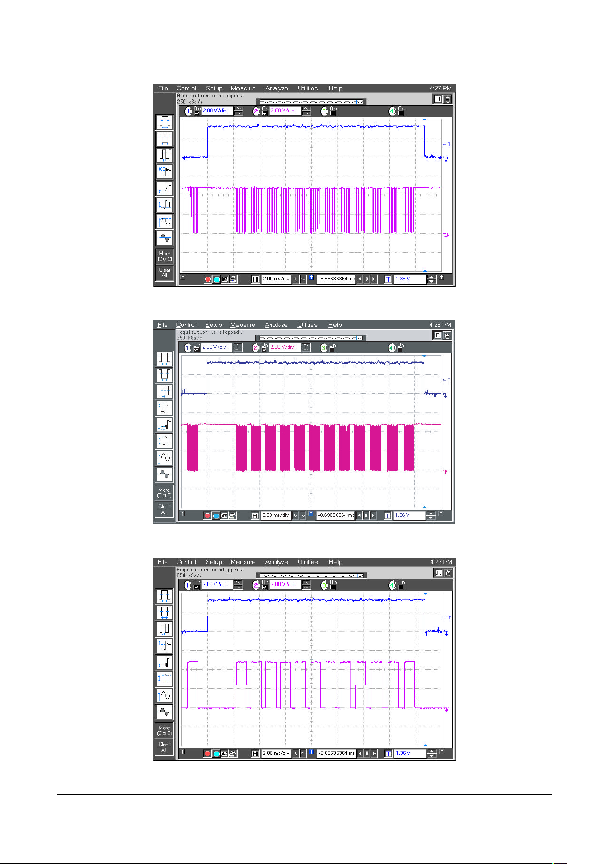
(1) Checking Y S /W
Figure 3. Connecting The Logic Main Board and The Test JIG Board
Figure 4. Connecting Oscilloscope Probe 1 (Trigger)
Page 58
Circuit Operation Description
Samsung Electronics 5-37
! Connect Probe 2 to LY1 30 of The JIG Board (8 (LE-Y) of The Logic Main Board F2016).
# Connect Probe 2 to LY1 25 of The JIG Board (6 (TCS_Y) of The Logic Main Board F2016).
@ Connect Probe 2 to LY1 28 of The JIG Board (7 (STB_Y) of The Logic Main Board F2016).
Page 59
Circuit Operation Description
5-38 Samsung Electronics
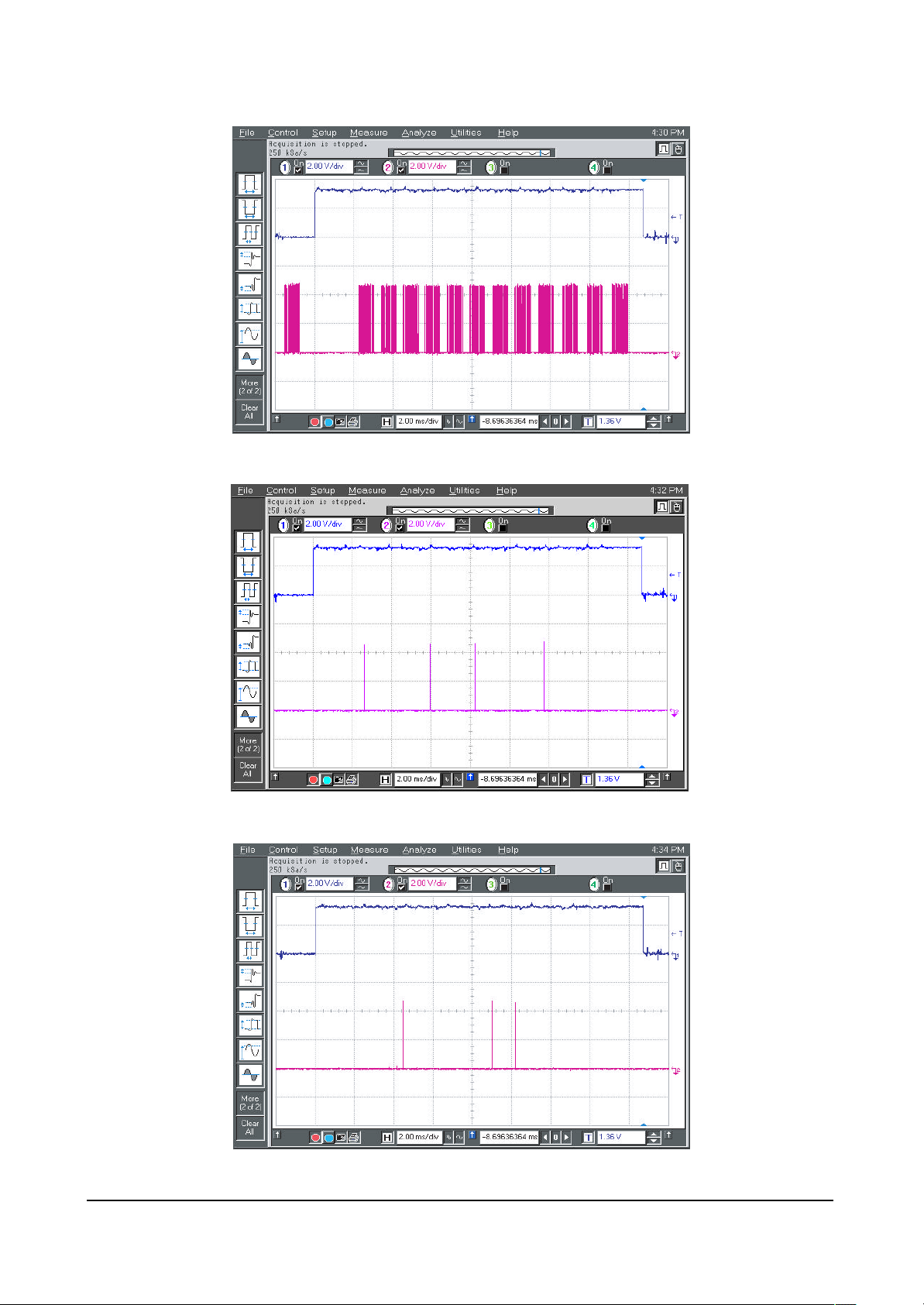
$ Connect Probe 2 to LY1 24 of The JIG Board (5 (CLK_Y) of The Logic Main Board F2016).
^ Connect Probe 2 to LY1 20 of The JIG Board (7 (SIA) of The Logic Main Board F2016).
% Connect Probe 2 to LY1 21 of The JIG Board (8 (SIB) of The Logic Main Board F2016).
Page 60
Circuit Operation Description
Samsung Electronics 5-39
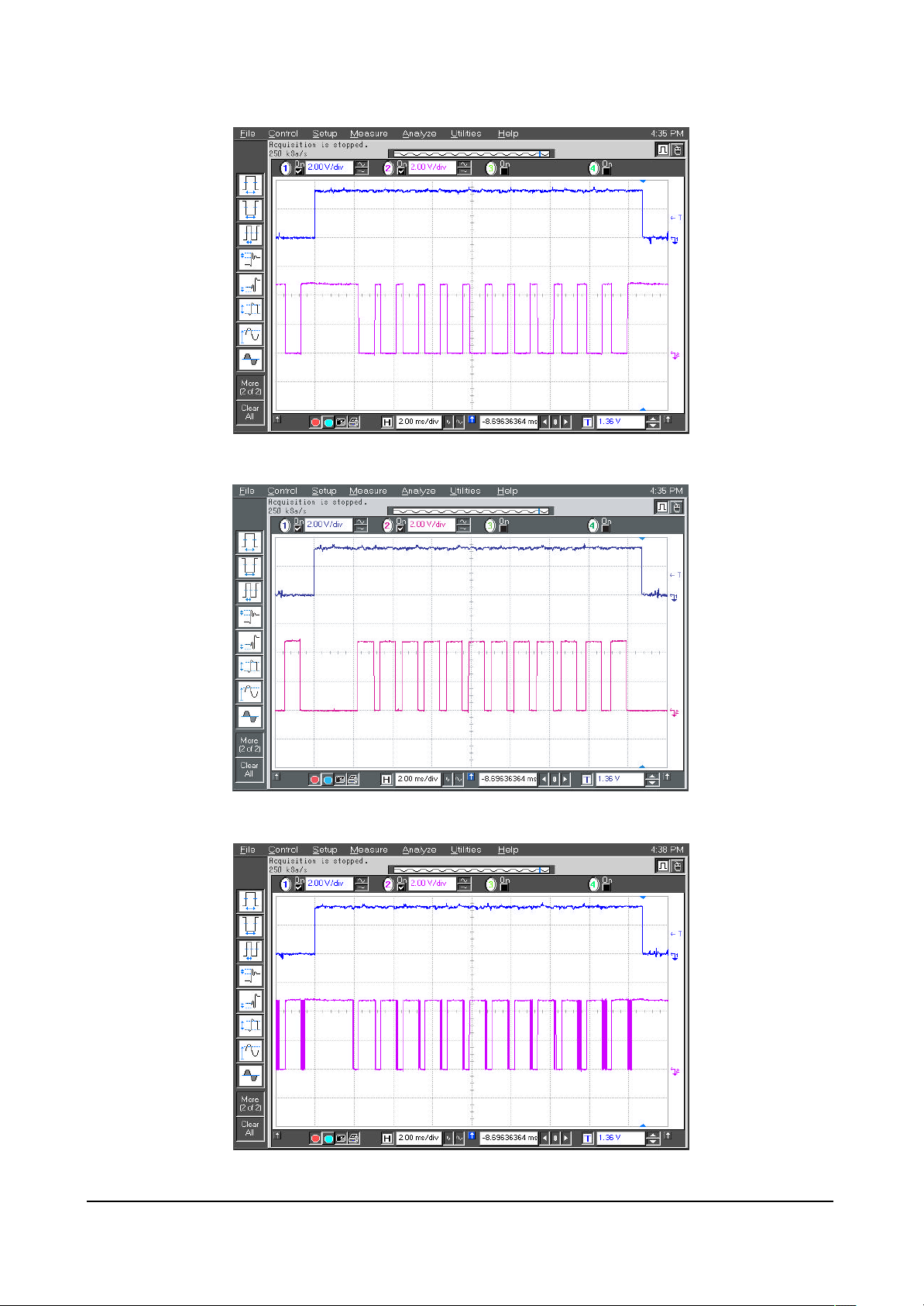
& Connect Probe 2 to LY1 14 of The JIG Board (5 (YSP) of The Logic Main Board F2016).
* Connect Probe 2 to LY1 13 of The JIG Board (6 (YSC) of The Logic Main Board F2016).
( Connect Probe 2 to LY1 10 of The JIG Board (7 (YER) of The Logic Main Board F2016).
Page 61
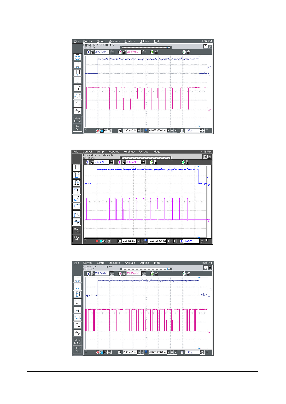
Circuit Operation Description
5-40 Samsung Electronics
) Connect Probe 2 to LY1 9 of The JIG Board (8 (YP) of The Logic Main Board F2016).
1 Connect Probe 2 to LY1 8 of The JIG Board (6 (YRR) of The Logic Main Board F2016).
2 Connect Probe 2 to LY1 5 of The JIG Board (5 (YG) of The Logic Main Board F2016).
Page 62
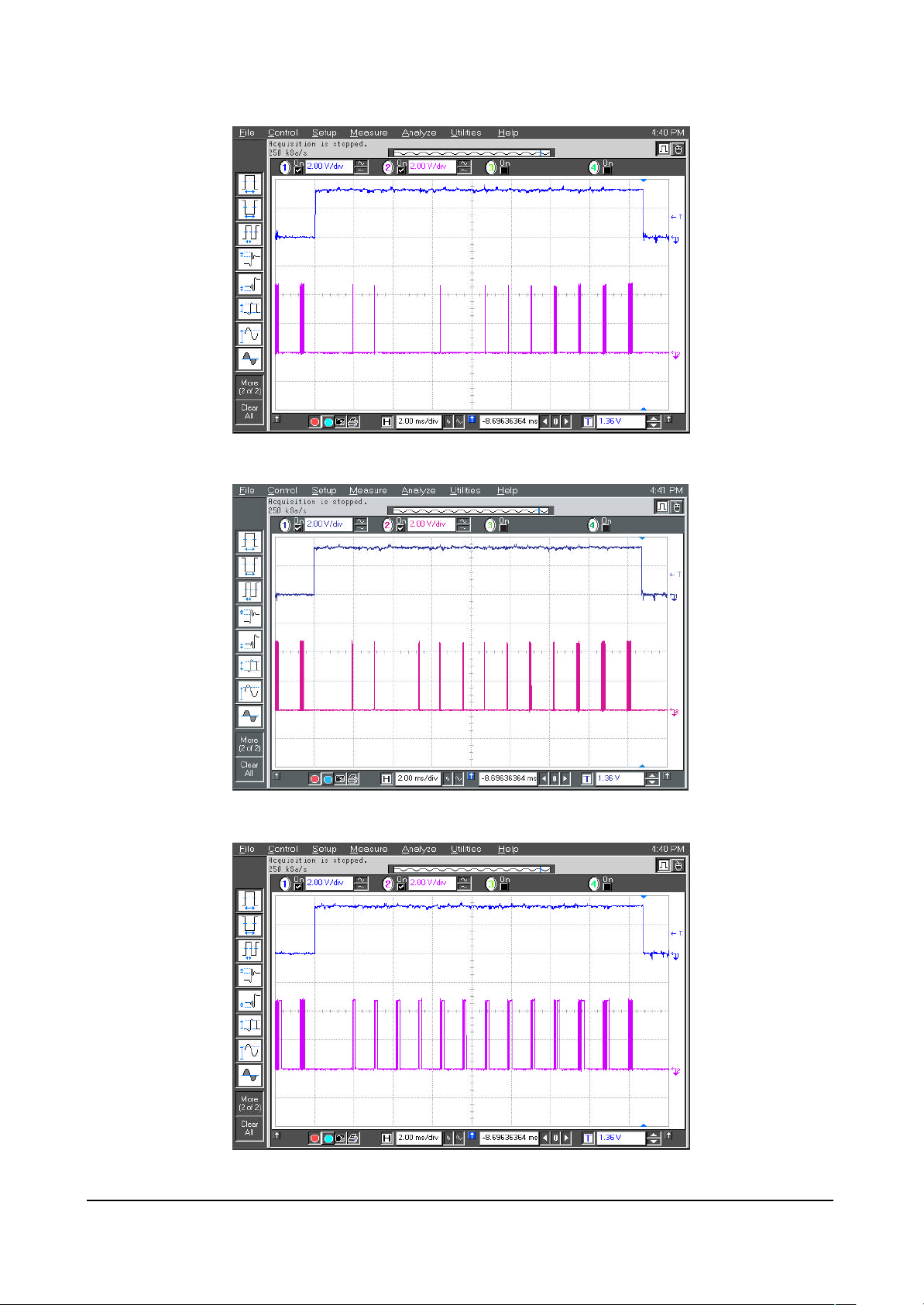
Circuit Operation Description
Samsung Electronics 5-41
3 Connect Probe 2 to LY1 4 of The JIG Board (8 (YF) of The Logic Main Board F2016).
4 Connect Probe 2 to LY1 2 of The JIG Board (6 (YR) of The Logic Main Board F2016).
5 Connect Probe 2 to LY1 1 of The JIG Board (5 (YS) of The Logic Main Board F2016).
Page 63
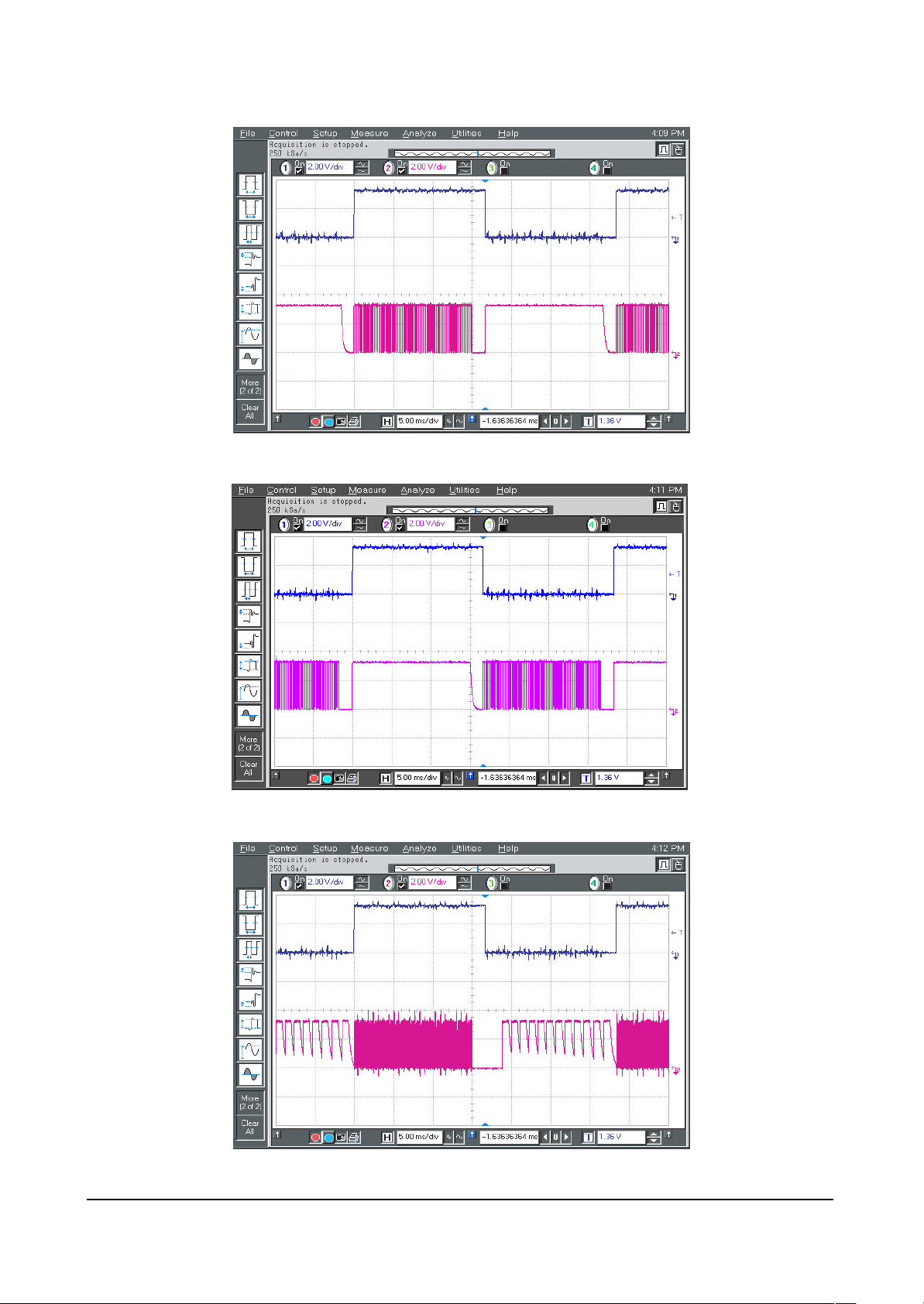
Circuit Operation Description
5-42 Samsung Electronics
6 Connect Probe 2 to 1 and 72 of IC2005, and Check The Following Waveform Shows at Oscilloscope.
7 Connect Probe 2 to 1 and 72 of IC2006, and Check The Following Waveform Shows at Oscilloscope.
8 Connect Probe 2 to 1 and 81 of IC2007, and Check The Following Waveform Shows at Oscilloscope.
Page 64
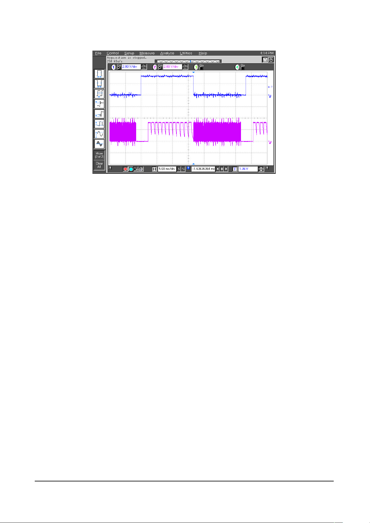
Circuit Operation Description
Samsung Electronics 5-43
9 Connect Probe 2 to 1 and 81 of IC2008, and Check The Following Waveform Shows at Oscilloscope.
Page 65
Circuit Operation Description
5-44 Samsung Electronics
! Connect Probe 2 to LX1 2 of The JIG Board (6 (XRR) of The Logic Main Board F2016).
@ Connect Probe 2 to LX1 4 of The JIG Board (7 (XR) of The Logic Main Board F2016).
# Connect Probe 2 to LX1 6 of The JIG Board (8 (XS) of The Logic Main Board F2016).
(1) Checking X S /W
Page 66
Circuit Operation Description
Samsung Electronics 5-45
$ Connect Probe 2 to LX1 8 of The JIG Board (5 (XF) of The Logic Main Board F2016).
% Connect Probe 2 to LX1 10 of The JIG Board (6 (XG) of The Logic Main Board F2016).
Page 67
Circuit Operation Description
5-46 Samsung Electronics
■ 42°”SD logic buffer board T/S
Required test equipment : -.Oscilloscope (digital 400 MHz 2 channel or more)
Other equipment : -.DC power supply (5V : 1EA )
-.Multi meter
-.Logic board : 1EA
-.Sub-PCB ASS'Y for JIG: 1 EA
(1) First, perform eye-inspection and short circuit inspection for the power stage of the logic board to
examine. Then, perform the following examinations on the board in order if no problem was found.
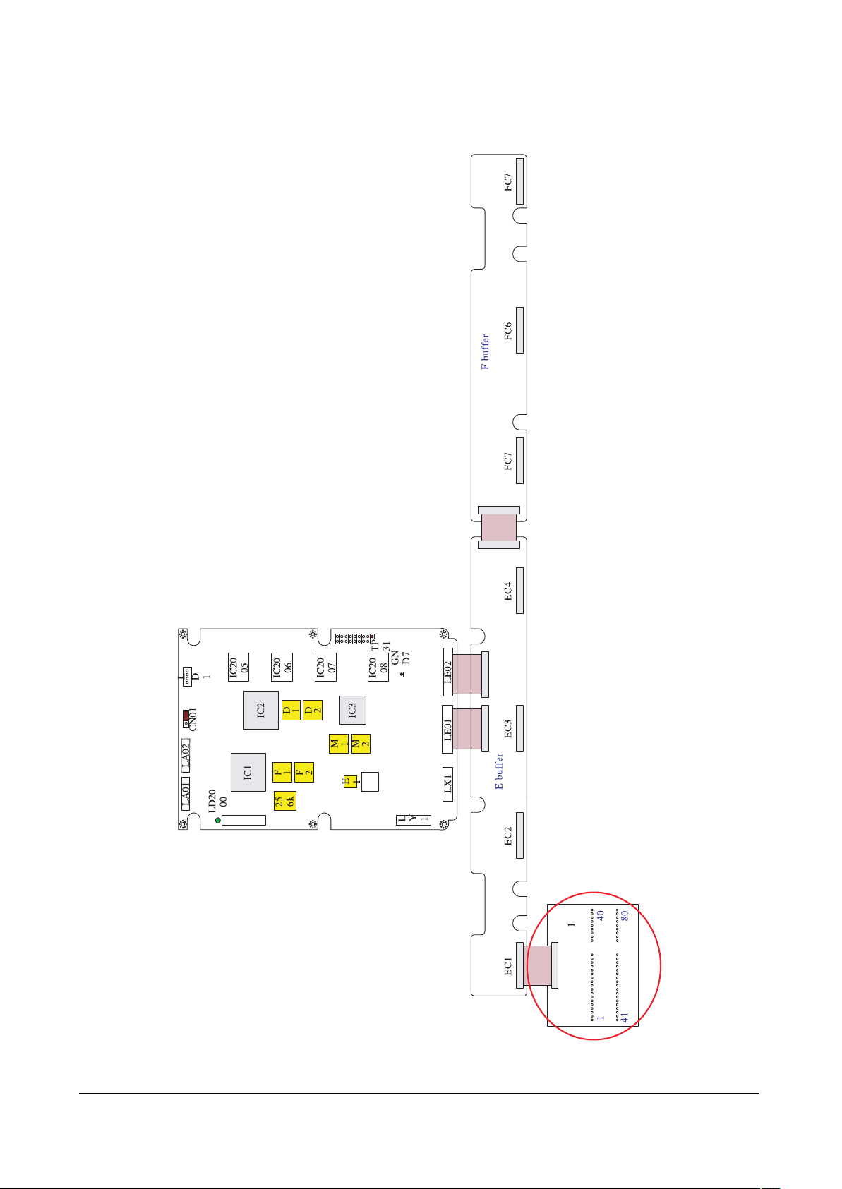
(2) If no problem was found in step ®ÿ, connect buffer board as Figure 5 shows, connect sub-PCB for
COF data check and replace 256K EEPROM with Test EERPOM for the logic board to output fullwhite pattern.
(3) Supply 5V to the logic board, and check that the LED on the left-top of the board blinks at about 1 sec-
ond interval. If no problem is found, measure the output waveform of sub-PCB, and compare it with
that of normal state.
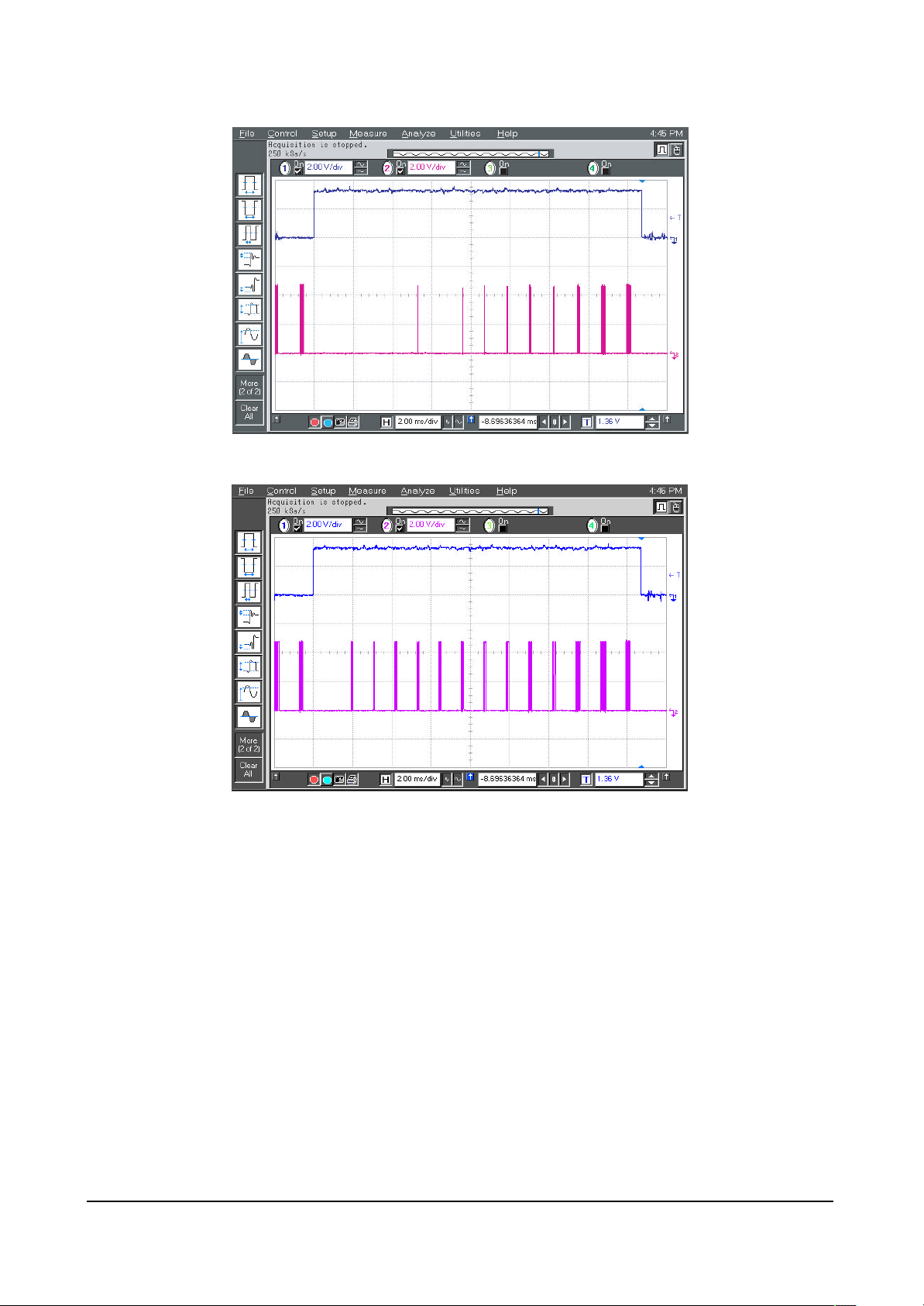
(4) Check EC1, EC2, EC3, EC4, FC5, FC6, and FC7 in order. You can only examine doubtable waveform
selectively.
(5) Set probe 1 of oscilloscope to trigger signal, and connect it to the TP31 of the logic board.
(6) Set oscilloscope to 2ms/div. After adjusting probe 2 to 5V/div, check output signal zooming important
points.
(7) Appended waveform is for full-white input pattern. Output waveform when each of R, G and B pat-
tern is supplied individually is summarized in the following table.
❈ For short check, it would be better to test waveform in the order of R, G and B pattern.
R0(TP13,TP49), R1(TP16,TP52), G0(TP14,TP50), G1(TP17,TP53),
B0(TP15,TP51), and B1(TP18,TP54) in The JIG Board
(8) After T/S, turn off the power supply, and disconnect the connector. Record the result on the examina-
tion sheet.
Output waveform for the applied pattern
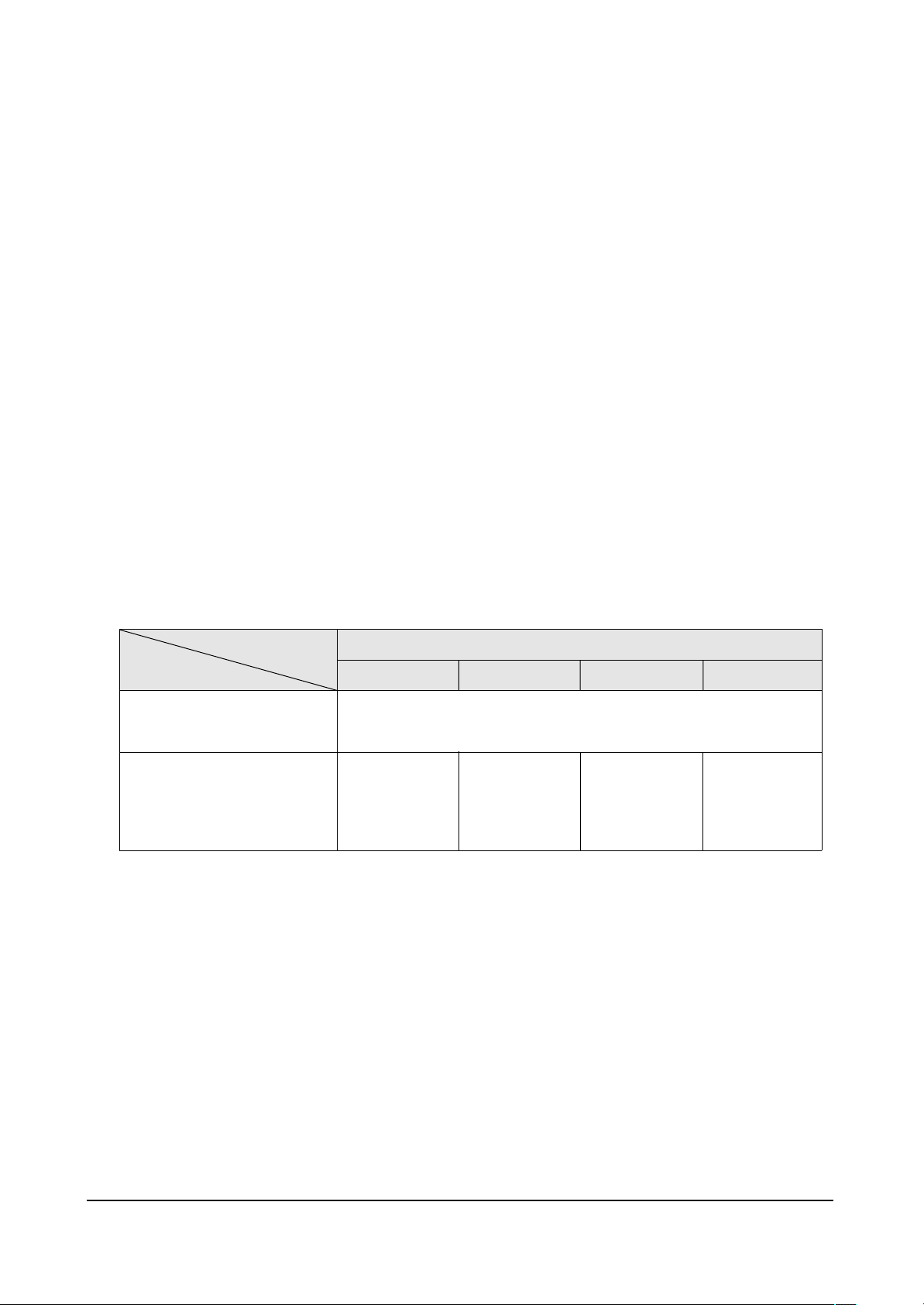
Full-white R G B
The same as the attached waveform
Control signal output of
sub-PCB for COF data check
R, B, G data signal output of
sub-PCB for COF data check
The output waveforms of all of the
R, G, B TP’s are the
same as the
attached waveform.
The output waveforms of all of the
R0, R1 TP’s are the
same as the
attached waveform.
The output waveforms of all of the
G0, G1 TP’s are the
same as the
attached waveform.
The output waveforms of all of the
B0, B1 TP’s are the
same as the
attached waveform.
Page 68
Circuit Operation Description
Samsung Electronics 5-47
Figure 5. 42” Single logic buffer
Page 69
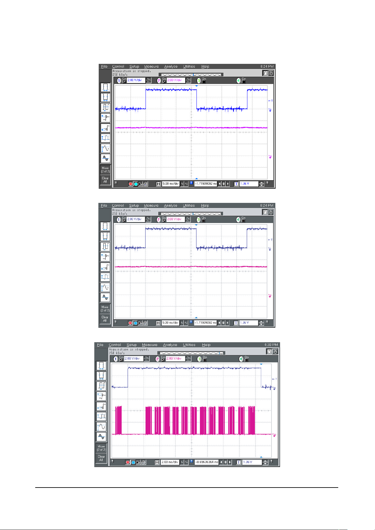
Circuit Operation Description
5-48 Samsung Electronics
! TP 13 ~ 18, 49 ~ 54 of The Test JIG Board
@ 21, 57 of The Test JIG Board
# 24, 31, 60, 67 of The Test JIG Board
(3) Checking buffer data
Page 70
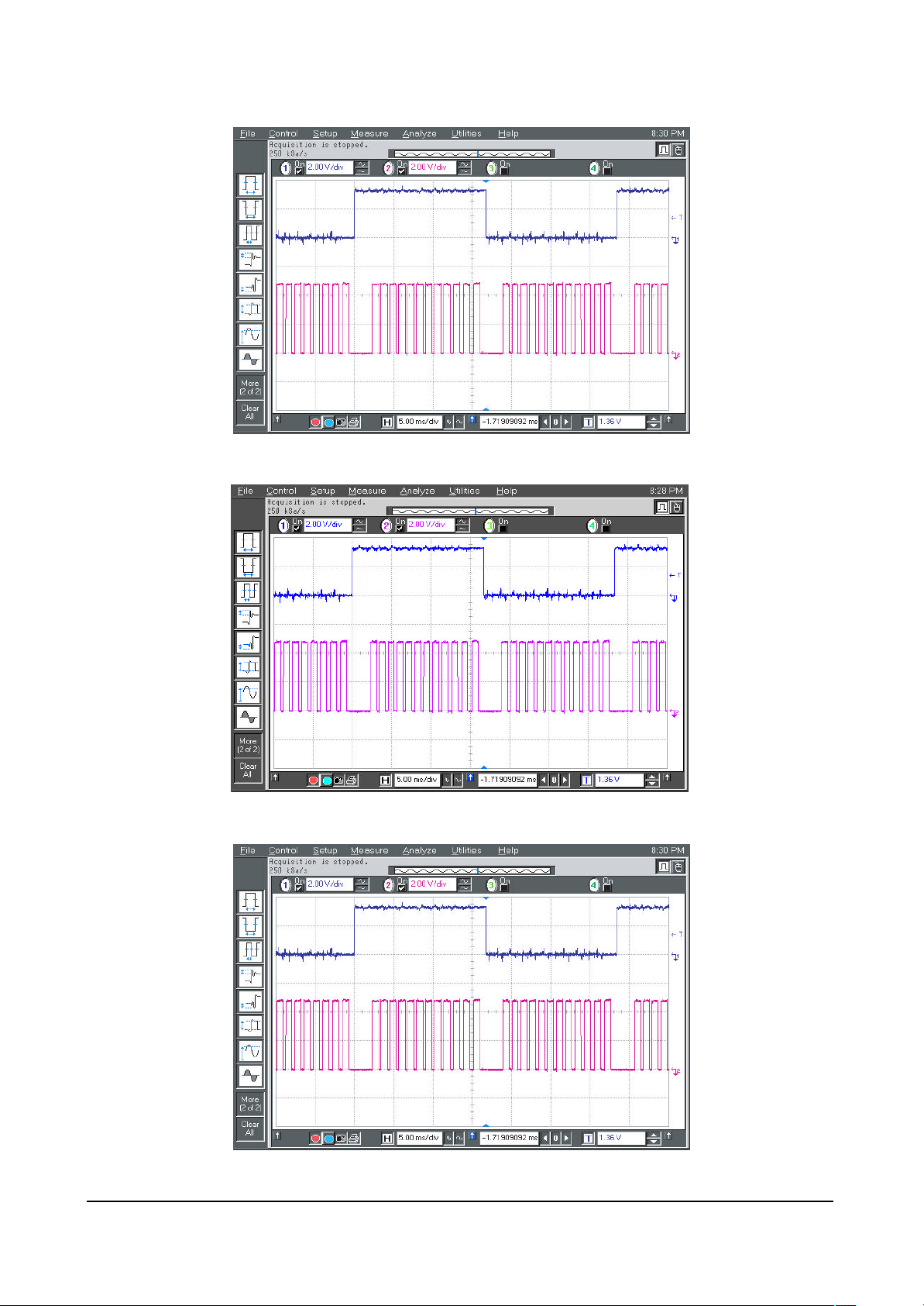
Circuit Operation Description
Samsung Electronics 5-49
$ TP 25, 32, 61, 68 of The Test JIG Board
% TP 19, 26, 55, 62 of The Test JIG Board
^ TP 20, 27, 56, 63 of The Test JIG Board
Page 71
Circuit Operation Description
5-50 Samsung Electronics
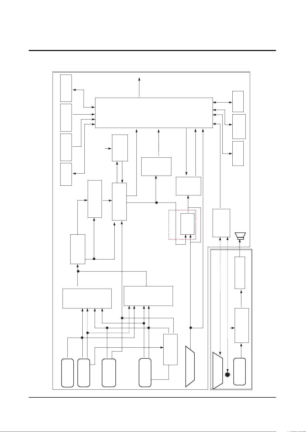
5-4 Block Diagram
5-4-1 42” Monitor Scaler Block Diagram
IR
Key
LED
RE[7:0]
GE[7:0]
BE[7:0]
PROTECT
LVS
IR ,LED
Output CLK
DIS. OSC.
EEPROM
Key Matrix
)
hz
130M
(
)
Mh z
26
(
24C16
MCKEXT
<Image
DCKEXT
CLK2
I2C(1)
I2C
V_Y/ G V_Pr / R
V_Pb/B
DAC
SDA9280
LHS
Pr oces sor >
Image Scaling
Pul se
Sandcast l e
SCP
H, V
CXA2101AQ
RGB Matrix
LENG
DCL K
I2C
RTC
PCF8563
364
CPU
With
OSD M i x er
Frame Rat e
Conversi on
PW
V
G
Fl ash
Mem ory
29LV160
(CPLD)
VG[ 7: 0]
VR[ 7: 0]
VB[ 7: 0]
VHS
4A3
M
VCLK
SRAM
616V1000
KM
PLL
ADC
With
VS_OUT 1
AD988 4
HS_OUT1
R, G, B_OUT,
SR[ 23: 0] , SQ[23: 0]
MHS, P CLK , SOG
CKI NV, CLAMP
MHSYNC, MCOAST
ADC
PLL
Wi th
AD9 88 4
TXD/ RXD
YIN [ 7: 0]
UVI N[ 7: 0]
RCA OPTI ON
I2C
SDA9400
Pr ogr essi ve
CLK2
Y [7: 0]
LLC1
UV [ 7 : ]
H1 _OUT
V1_OUT
I2C
Video
MAI N
CVBS, Y
Decoder
I VVS
IVHS
VPC3 230
YP r P b( DV D)
YPr Pb( DTV)
PIP
Video
CVBS
R, G, B, FB
Decoder
FI FO
VPC3 230
Y
DT V
Y
DVD
BA7657
PC_R. G. B.
SW
AX232A
Ser i al
M
SCART OPTI ON
CHSYNC
CVSYNC
PC_H, PC_V
or Audio
Sub PCB f
p.
Am
o
Au di
(TA1101)
C
o
2
429S )
I
7
Au di
Pr ocessor
(TDA
ADC
CVBS
eo
Vid
( CVBS)
MA IN_Y
MA IN_C
S1_DET
deo
(Y/C)
S-Vi
RCA
ponent
Input
Com
DVD VPC3230
( 480i )
DTV
t
Scar
PCF8591
I2C
nput
I
PC
#8 I D
(15pin D-SUB)
PC_R, PC_G, P C_B,
PC_H, PC_V
RS232C
( 9pi n,MALE)
n
I
o
3( L/R)
Au di
RS- 232
Page 72
Circuit Operation Description
Samsung Electronics 5-51
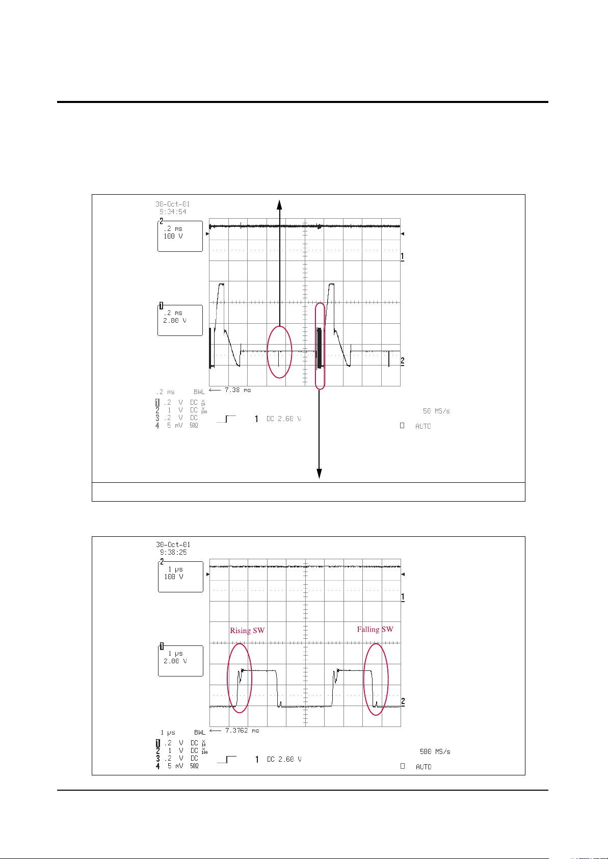
5-5 Major In/Out Signal Waveforms and Voltages of the Unit
5-5-1 In/Out Waveforms
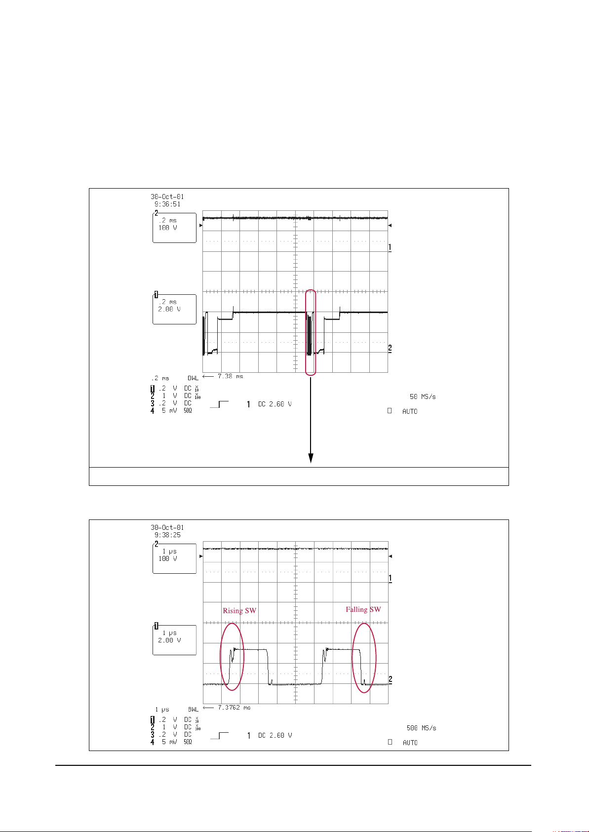
❏ Y output waveform
- It is the waveform when it is not connected to the panel.
* You should check that a single scan waveform is outputted!!!
Y output waveform (200us/div, 100V/div)
* You should check that energy recovery software is in operation!!!
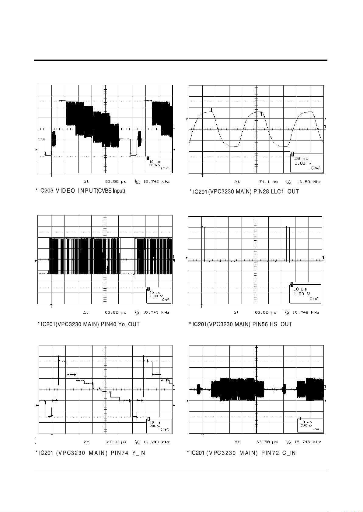
Page 73
Circuit Operation Description
5-52 Samsung Electronics
❏ X output waveform
- It is the waveform when it is not connected to the panel.
X output waveform (200us/div, 100V/div)
* You should check that energy recovery software is in operation!!!
Page 74
Circuit Operation Description
Samsung Electronics 5-53
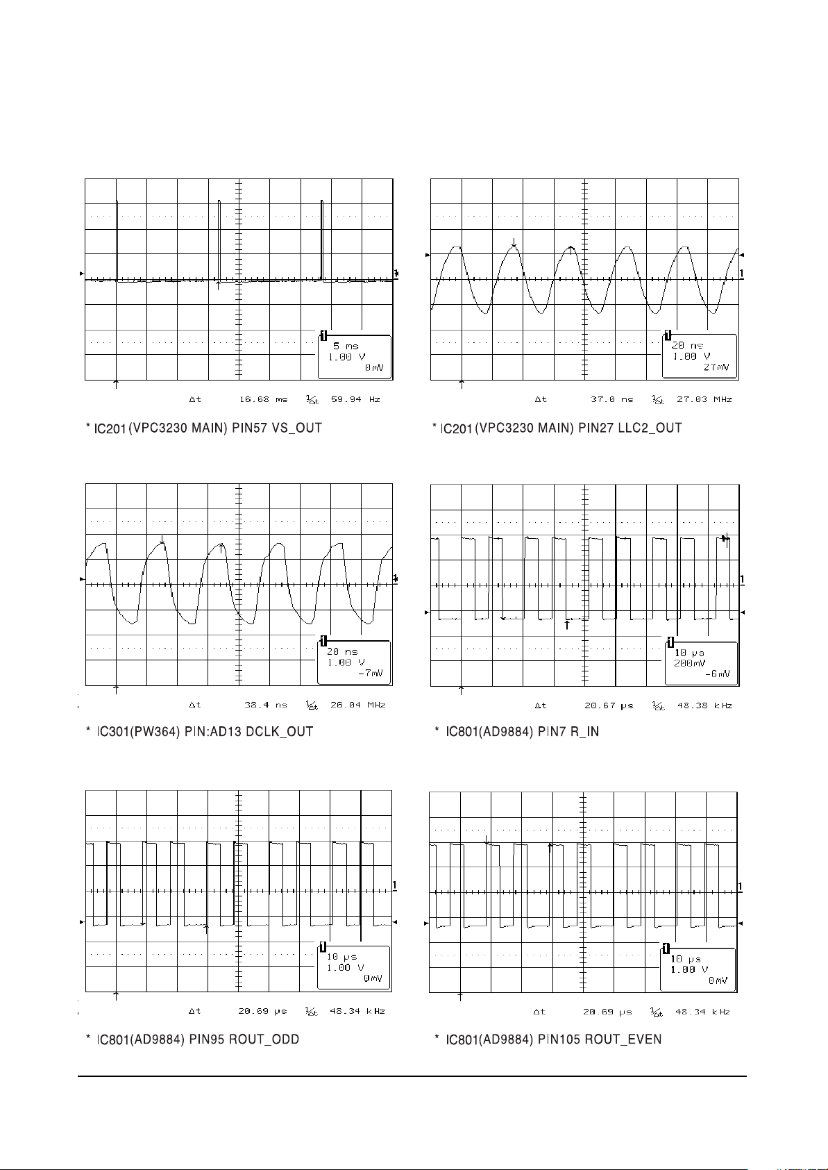
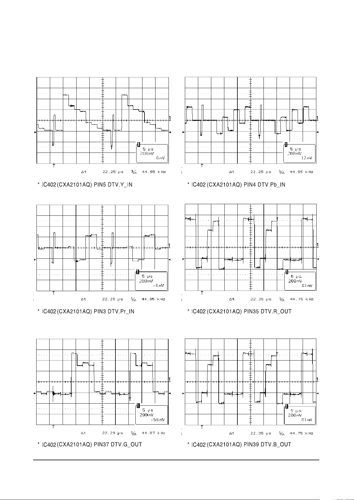
5-6 Main I/O signal pules and voltages
5-6-1 Signal Pulses of Image Board(Input Signal Conditions : 7 Color bar)
Page 75
Circuit Operation Description
5-54 Samsung Electronics
Page 76
Circuit Operation Description
Samsung Electronics 5-55
Page 77

5-56 Samsung Electronics
MEMO
Page 78

Circuit Operation Description
Samsung Electronics 5-57
Page 79
Troubleshooting
Samsung Electronics 6-1
6. Troubleshooting
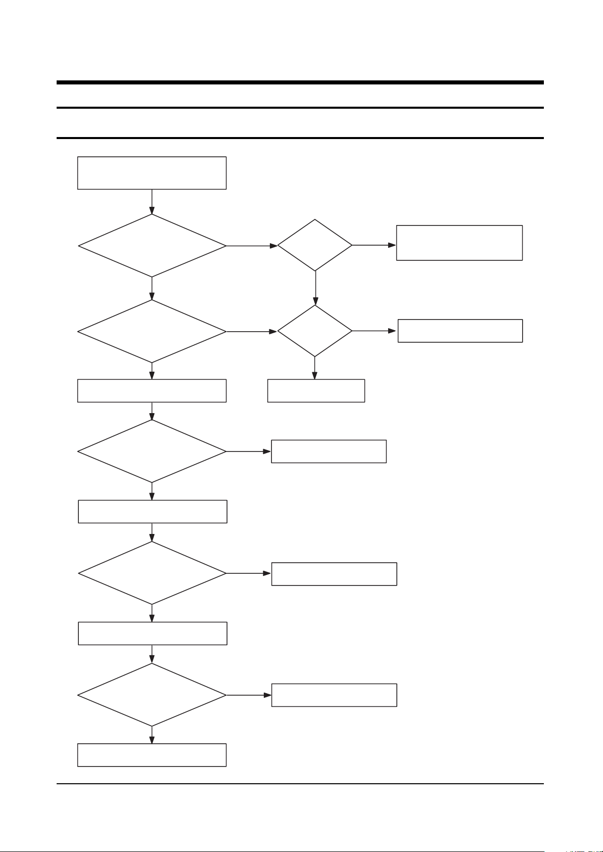
6-1 Entirely no screen
Remove SMPS output connector
(connect Video B d only)
Normal
Power on
Normal
SMPS Output
Voltage
Normal
Logic Connect Power
LED Light-on
(Power, Sink)
Normal
X-B d Connect Power
Abnormal
Abnormal
Abnormal
5V Output
Abnormal
AC Input
Normal
Replace SMPS
Replace Logic B d
Normal
Normal
Replace Video B d
Change Fuse
X-B d Output
Normal
Y-B d Connect Power
Y-B d Output
Normal
Replace Panel
Abnormal
Replace X-B d
Abnormal
Replace Y-B d
Page 80
6-2 Samsung Electronics
Alignment and Adjustments
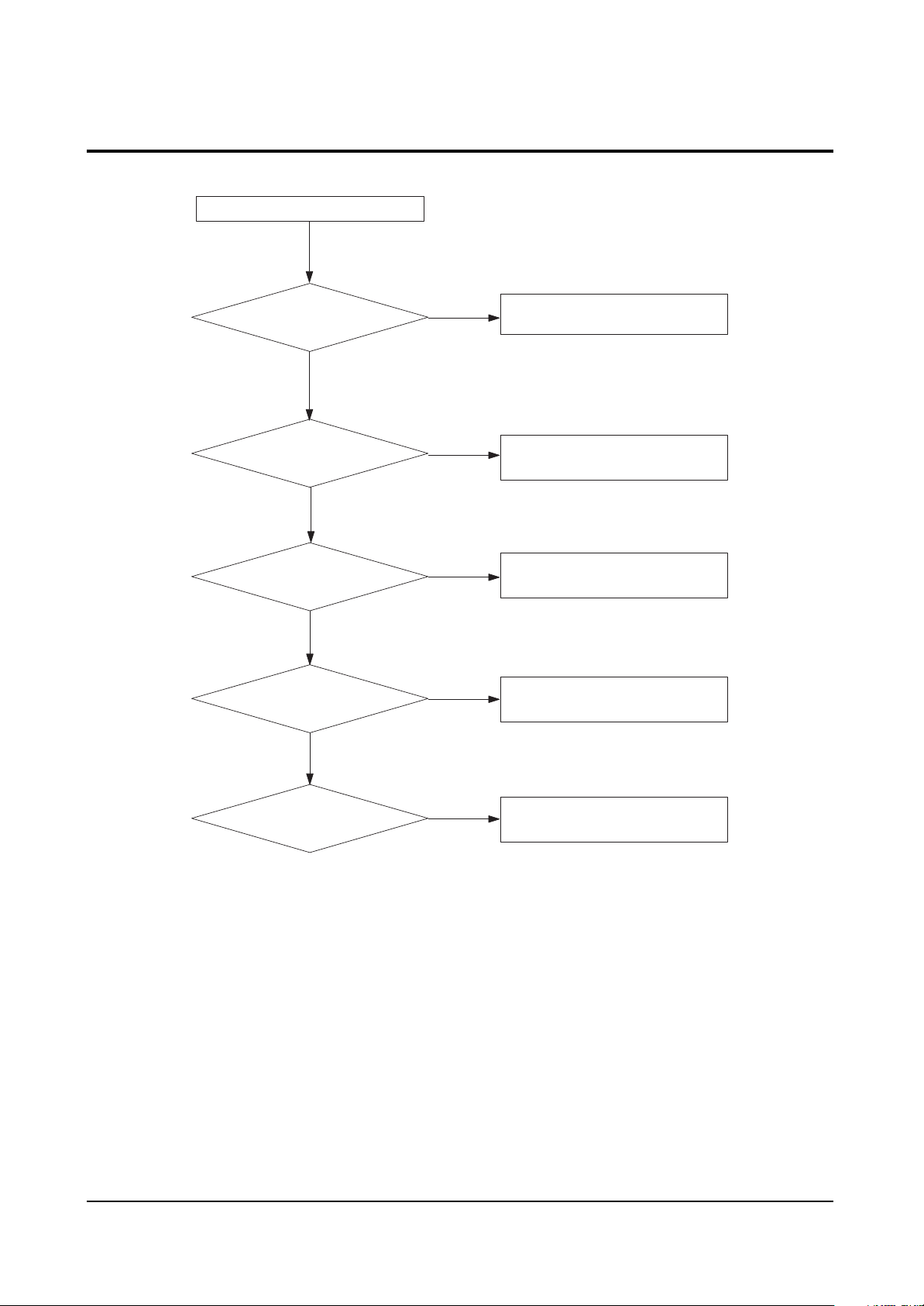
6-2 Partly no screen
Power on
Upper part no screen
No
Lower part no scree
No
1//14 Screen part
Abnormal
No
1/28 no screen
Yes
Yes
Yes
Yes
Replace Upper Scan Buffer B d
Replace Lower Scan Buffer B d
Replace Corresponding
Address Buffer B d
Replace Panel
No
1/7 no screen
Yes
Replace Panel
Page 81
Troubleshooting
Samsung Electronics 6-3
6-3 Checking the Board (Unit)
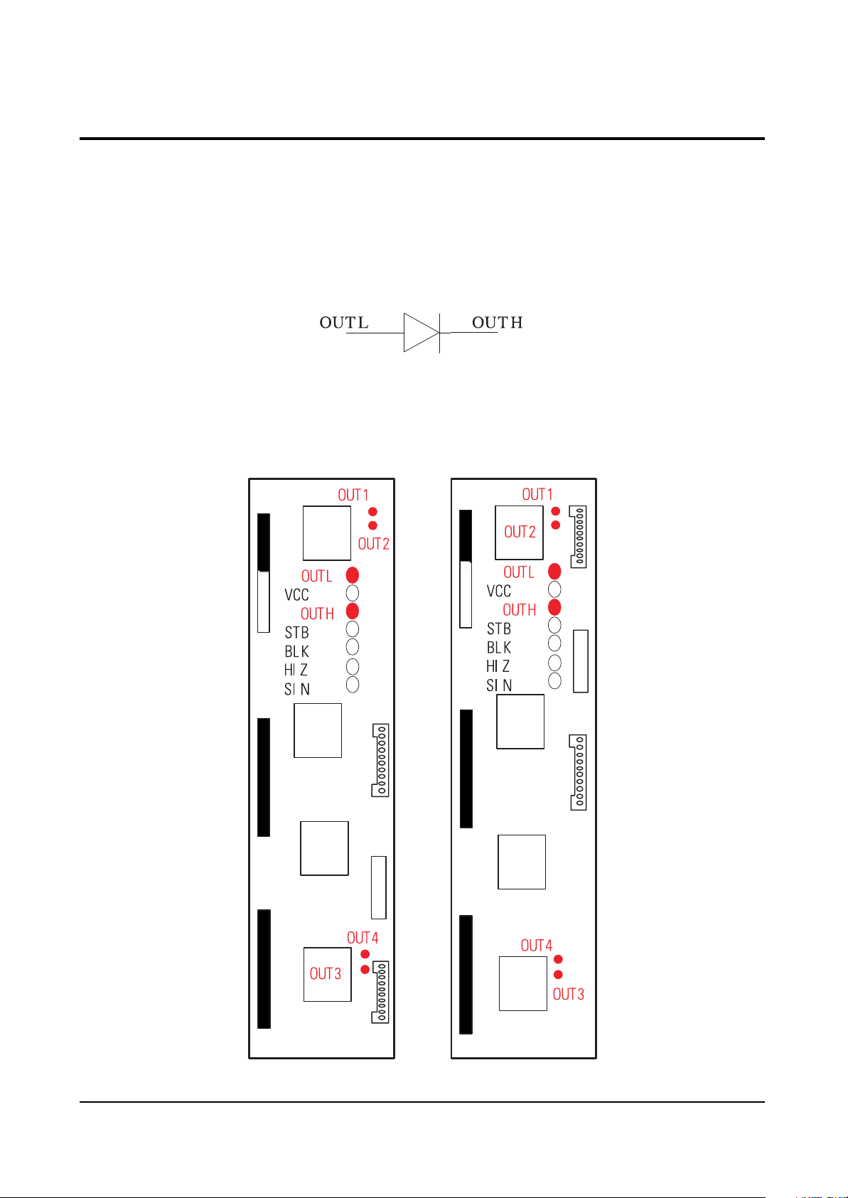
6-3-1 Y buffer
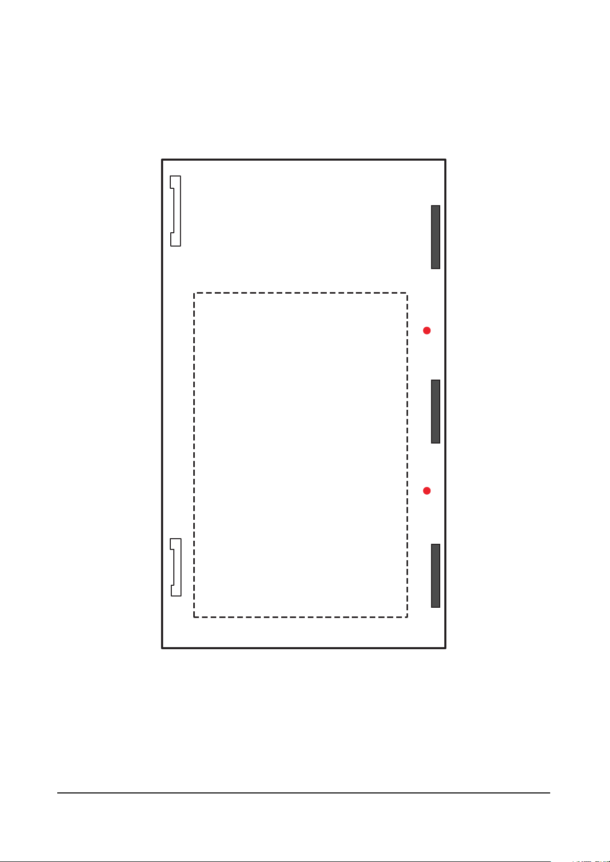
- To check the main board, you have to check the Y buffer first.
- After separating Y Main and Y buffer board,
- Check the Diode between OUTL and OUTH, and make sure that the forward voltage drop is between
0.4 and 0.5V.
- Check that the resistance between the two terminals is more than several kW.
Page 82
Troubleshooting
6-4 Samsung Electronics
6-3-2 Y Main
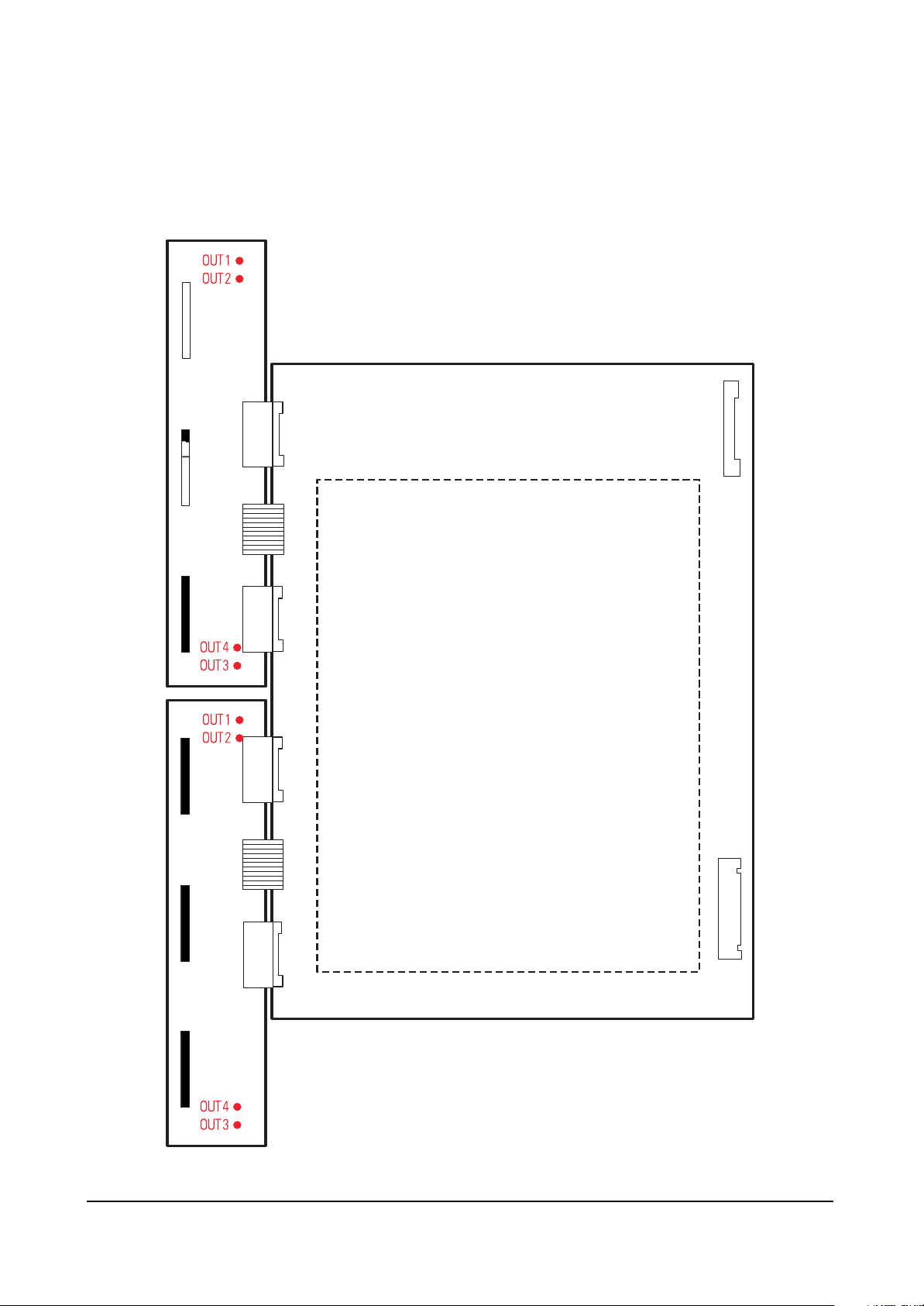
- After connecting Y main and Y buffer board, check that one of the output waveforms from OUT 1, 2, 3
or 4 is the same as that of the appendix 1 when power is supplied.
Page 83
Troubleshooting
Samsung Electronics 6-5
6-3-3 X Board
- Check that one of the output waveforms from X-OUT 1 or 2 is the same as that of the appendix 2
when power is supplied.
X- OUT1
X- OUT1
Page 84
Troubleshooting
6-6 Samsung Electronics
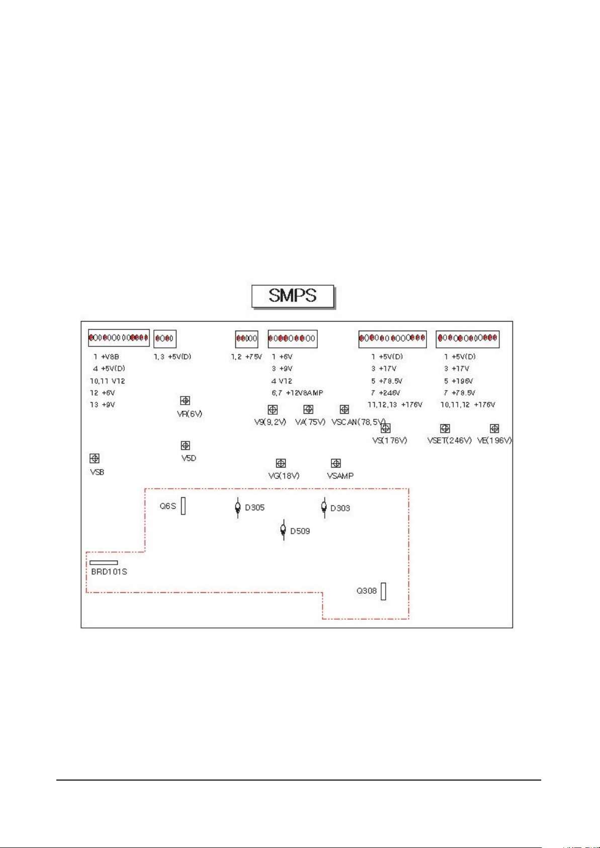
6-3-4 SMPS
- Check output voltage.
- If output voltage is not detected, check the following lists:
(1) Check fuse
(2) In case of +5V(D), check that D305 is short
(3) In case of VSAMP, check that D506 is short
(4) In case of VA, check that D303 is short
(5) In case of VS, check that pin 2 and 3 of Q303 are short
(6) In case of Q6S, check that pin 2 and 3 are short
(7) Check that BRD101S is short
Page 85

Troubleshooting
Samsung Electronics 6-7
6-3-5 Scaler Borad
1. PW364 Input Clock
(1) MCKEXT
Check IC406(IC502) pin 5.
Power on : MCKEXT = 97.5MHz
Standby : MCKEXT = 48.75MHz
(2) MCKEXT, DCKEXT
Check IC407(ICS502) pin 25. DCKEXT = 65MHz
(3) VCLK
Check IC203(SDA9400) pin 26. VCLK = 27MHz
(4) GCLK
Check IC401(AD9884) pin 115(TP404).
GCLK is differently seen according to PC input signal format(VGA, SVGA, XGA)
GCLK = 15MHz ~ 50MHz(This value is apparently half of the clock frequency of the relevant PC input signal format.
2. VPC3230
- Check power is supplied(5V, 3.3V).
- Check Reset(pin 15) is high.
- Check I
2
C-bus(pins 13, 14)
- Check the signal input to Y signal(pin73), C signal(pin 71), PLL DVD-Y signal (pin 72).
- Check the output clocks LLC1(pin 28), LLC2(pin 27). (LLC1 = 13.5MHz, LLC2 = 27MHz)
- Check the output H sync(pin 56) and check V sync(pin 57) is output.
- Check output digital data.
3. SDA9400
- Check power is supplied(3.3V).
- Check Reset(pin 30) is high.
- Check I
2
C-bus(pins 20, 21)
- Check clock is input.(pins 28, 54 : 27MHz. pin 29 : 13.5MHz)
- Check digital data input.
- Check the input H sync (pin 23) = 15.75MHz, V sync (pin 22) = 60Hz
- Check digital data input.
- Check the output H sync (pin 60) = 31.5KHz, V sync (pin 61) = 60Hz, VCLK (pin 26) = 27MHz
4. AD9884(IC101)
- Check power is supplied(3.3V)
- Check I
2
C-bus(pins 29, 30)
- Check PC signal, HD-component signal is input.
- Check the input signal GREF (pin 40). The GREF signal applies to a fixed form of the input H sync signal.
- Check the output signal GFBK (pin 117). The GFBK signal applies to a fixed form of PLLD H sync signal.
- Check the output signal GCLK (pin 115). The GCLK is differently seen according to the PC input signal format(VGA, SVGA, XGA).
GCLK = 15MHz ~ 50MHz This value is apparently half of the clock frequency of the relevant PC input signal format.
- Check digital data output.
Page 86

Troubleshooting
6-8 Samsung Electronics
5. AD9884(IC801)
- Check power is supplied(3.3V).
- Check I
2
C-bus(pins 29, 30)
- Check Video signal is input.
- Check the input signal 2HS (pin 40 or TP406)
- Check the output signal VHS (pin 117 or TP409)
- Check the output signal VCLK (pin 115 or TP408)
- Check digital data input.
6. PW364 Reset
- When the Reset switch is pressed. if OTP01(29LV160T) pin 28(TP151) undergoes ransition.
PW364 operates and OTP01 also does. Unless transition happens, it means PW364 is not operating.
7. PW364 Communication
- Operate the PC hyper terminal Settings are as follows :
Model Selection : Direct connect to com1
No. of Bit per second : 57600
Data Bit : 8
Parity : None
Stop Bit : 1
Flow Control : None
- Whenever the Reset switch is pressed, the following is displayed on the PC hyper terminal screen.
CBooter V1.5 & 2000.01.26
CBooter V1.5 & 2000.01.26
CBooter V1.5 & 2000.01.26
Page 87
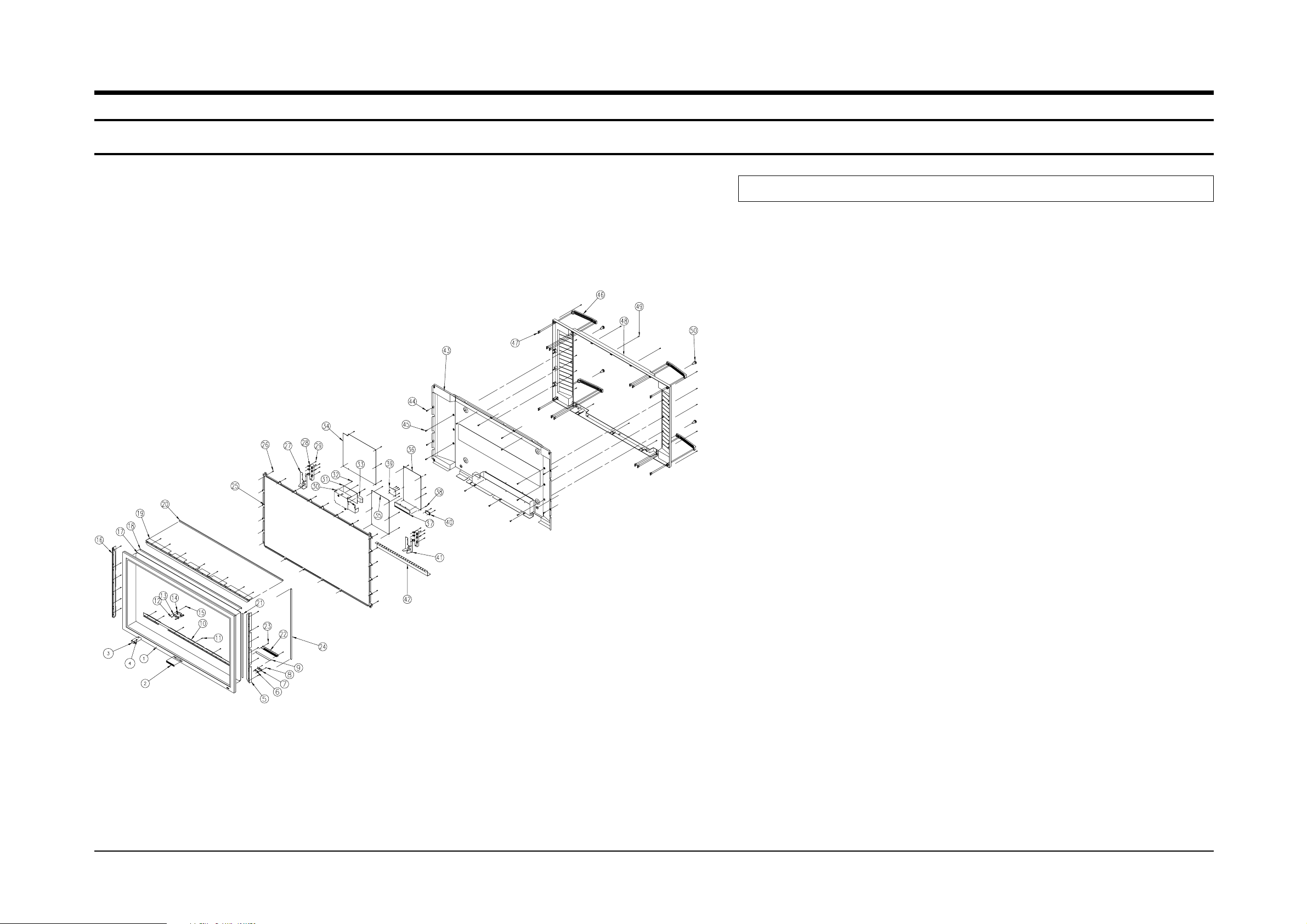
Exploded View & Parts List
Samsung Electronics 7-1
7. Exploded View & Parts List
7-1 PS42P2SDX/XEC
No Code No Description;Specification Q’ty Remark
1 AA64-01799C CABINET-FRONT;HIPS HB GRAY,KUJU 1
2 AA64-01560A BADGE-BRAND;AL FORGING,SAMSUNG SILVER 1
3 AA64-01566F KNOB-MASTER;ABS HB BLK #SV-012P 1
4 AA61-60003J SPRING-CS;SUS 304 1
5 AA61-01061A BRACKET-FILTER SIDE L,ASSY;AL 6063 EXT,T1.2 1
6 AA64-01549B WINDOW-RMC;ACRYL VIOLET 1
7 AA95-01837F ASSY SUB-PCB,REMOCON;SPD-42P2S,D51A,AA95 1
8 6003-000333 SCREW-TAPTITE;M3 * L10 YEL 2
9 AA95-01751D ASSY SUB-PCB CONTROL;PS42P2S,D53A,AA95-0
10 AA61-01062A BRACKET-FILTER BOT,ASSY;AL 6063 EXT,T1.2 1
11 6003-001020 SCREW-TAPTITE;RH,+,B,M4,L10,ZPC(YEL) 28
12 6006-001035 SCREW-ASSY,MACHINE;WSP,PH,M3*L8YEL 2
13 AA95-01833D ASSY SUB-PCB,POWER ON/OFF;SPD-42P2S,D51A 1
14 AA61-00716B BRACKET-POWER;,SECC,T1.0 1
15 6003-001026 SCREW-TAPTITE;RH,+,B,M4*L15 2
16 AA61-01060A BRACKET-FILTER SIDE R,ASSY;AL 6063 EXT,T1.2 1
17 AA67-00112A MIRROR-GLASS;42INCH,P1S,MESH,55% 1
18 AA72-00017A SPONGE-EMI,FILTER;SHIELD-FORM,T1.2,D10,L980 2
19 AA61-01059A BRACKET-FILTER TOP,ASSY;AL 6063 EXT,T1.2 1
20 AA60-00110C SPACER-FILTER;42P2,P/U V0,L,BLK 2
21 AA72-00018A SPONGE-EMI,FILTER;SHIELD-FORM,T1.2,D10,L560 2
22 AA63-00433A COVER-BOT;42P2S,ABS HB,BLK,SV012P 1
23 6003-001026 SCREW-TAPTITE;RH,+,B,M4,L15,ZPC(BLK),SWRCH18 2
24 AA60-00110D SPACER-FILTER;42P2,P/U V0,L,BLK 2
25 AA98-00231A ASSY-PANEL,PDP;PS-42P2S,D53A 1
26 6003-001026 SCREW-TAPTITE;RH,+,B,M4,L15,ZPC(BLK),SWRCH18 26
27 AA61-01054A BRACKET-COVER,RIGHT;PDP,AL 5051,T1.5 1
28 AA61-00584B GUIDE-STAND;AL DIECASTING 2
29 6006-001039 SCREW-ASSY,MACHINE;WSP,PH,M4*L12YEL 12
30 AA61-00582C BRACKET-LINE,FILTER;SPC T1.0 1
31 AA95-01819A ASSY SUB-PCB,LINE FILTER;PS42P2S,D53A,AA 1
32 6006-001035 SCREW-ASSY,MACHINE;WSP,PH,M3*L8YEL 6
33 2901-001222 FILTER-EMI AC LINE;22000PF,24X50X62.3MM 1
34 AA98-00188A ASSY-PBA,SMPS;SPD-42P2S,D51A,42SD 1
35 AA98-00241A ASSY-PBA,L-MAIN;,42SD,D53A,LJ41-00778A,S 1
36 AA95-01839A ASSY SUB-PCB,SCALER;PS42P2S,D53A,AA95-01 1
37 SHIELD-SCALER,BOT;SPTE T0.25 1
38 6006-001035 SCREW-ASSY,MACHINE;WSP,PH,M3*L8YEL 6
39 AA95-01844M ASSY SUB-PCB,SOUND;PS42P2S,D53A,AA95-013 1
40 AA95-01770A ASSY SUB-PCB TERMINAL;PS42P2S,D53A,AA95- 1
41 AA61-01055A BRACKET-COVER,LEFT;PDP,AL 5051,T1.5 1
42 AA63-00491B COVER-TERMINAL,TV;SUS 304,T0.5 1
43 AA63-00232A COVER-BACK,ASSY;AL T1.2,PS-42P2S 1
44 6003-001019 SCREW-TAPTITE;RH,+,B,M4,L12,ZPC(BLK),SWRCH18 13
45 6003-001020 SCREW-TAPTITE;RH,+,B,M4,L10,ZPC(YEL),SWRCH18 6
46 AA64-01551B HANDLE-SET;ABS,HB,BLK 4
47 6003-001026 SCREW-TAPTITE;RH,+,B,M4*L15 24
48 AA64-01802A CABINET BACK;HIPS V2 BLK 42P2S 1
49 AA60-10050T SCREW-TAPPING;SWRCH18A,M4,L20,RH,+,2S,-,ZPC 16
50 6006-001112 SCREW-ASS’Y MACH;WP,PH,+,M8,L16,ZPC,SWRCH18A 4
Page 88
Electrical Parts List
Samsung Electronics 8-1
8-1 PS42P2SDX/XEC
ASSY CHASSIS
1 * AA91-01674AASSY CHASSIS;PS42P2SDX/XEC S.N.A
..2 AA95-01770AASSY SUB-PCB TERMINAL;PS42P2S,D53A,AA95...3 CN603A 3711-003043 CONNECTOR-HEADER;BOX,4P,1R,2.5mm,STRAIGH
...3 JK603 AA63-40258ATERMINAL-SPEAKER;4P,ABS,4,-,-,-,BLK
...3 PCB AA41-00373APCB-SPK TERMINAL;SPD-50P2HM,CEM-1,1L,A,1 S.N.A
...3 SPK AA39-00294ALEAD CONNECTOR ASSY;PDP,UL1007#22,UL/CSA
...3 0202-000187 SOLDER-WIRE FLUX;-,RS60S,D1.2,63Sn/37Pb S.N.A
..2 AA95-01819AASSY SUB-PCB,LINE FILTER;PS42P2S,D53A,AA
...3 BLF+LF 6001-000516 SCREW-MACHINE;PH,+,M3,L10,ZPC(YEL),SM20C
...3 CN812 3711-000203 CONNECTOR-HEADER;1WALL,3P,1R,3.96MM,STRA
...3 CX811S 2306-000321 C-FILM,MPPF;470NF,5%,275V,TP,-,22.5
...3 CX812S 2306-000321 C-FILM,MPPF;470NF,5%,275V,TP,-,22.5
...3 CX813S 2306-000321 C-FILM,MPPF;470NF,5%,275V,TP,-,22.5
...3 CY811S 2201-000446 C-CERAMIC,DISC;3.3nF,20%,400V,Y5U,TP,15x
...3 CY812S 2201-000446 C-CERAMIC,DISC;3.3nF,20%,400V,Y5U,TP,15x
...3 CY813S 2201-000446 C-CERAMIC,DISC;3.3nF,20%,400V,Y5U,TP,15x
...3 CY814S 2201-000446 C-CERAMIC,DISC;3.3nF,20%,400V,Y5U,TP,15x
...3 CY815S 2201-000446 C-CERAMIC,DISC;3.3nF,20%,400V,Y5U,TP,15x
...3 CY816S 2201-000446 C-CERAMIC,DISC;3.3nF,20%,400V,Y5U,TP,15x
...3 EMI 2901-001222 FILTER-EMI AC LINE;250V,10A,UL,CSA,D,N,S
...3 FS811A 3602-000114 FUSE-HOLDER;-,-,30mohm
...3 FS811B 3602-000114 FUSE-HOLDER;-,-,30mohm
...3 FS811S 3601-001165 FUSE-CARTRIDGE;250V,8A,TIME-LAG,CERAMIC,
...3 LS812S AA27-00189ACOIL CHOKE;-,HPL5025M,20UH,10%,0.03OHM,7
...3 LS813S AA27-00189ACOIL CHOKE;-,HPL5025M,20UH,10%,0.03OHM,7
...3 LX811S AA29-00017AFILTER LINE NOISE;,25-4MH 7A,0.1OHM,1.5K
...3 LX812S AA29-00017AFILTER LINE NOISE;,25-4MH 7A,0.1OHM,1.5K
...3 PCB AA41-00574APCB-LINE FILTER;PS-42P2S,CEM-1,1L,A,1.6T S.N.A
...3 PCB+BL 6006-001035 SCREW-ASS’Y MACH;WSP,PH,+,M3,L8,ZPC(YEL) S.N.A
...3 PD811S 3711-000203 CONNECTOR-HEADER;1WALL,3P,1R,3.96MM,STRA
...3 RX811S 2002-001021 R-COMPOSITION;560KOHM,10%,1/2W,AA,TP,3.7
...3 VX811S 1405-000152 VARISTOR;560V,2500A,14x8.5mm,TP
...3 AA61-00582C BRACKET-LINE,FILTER;SPD-42P2H,SPC,T1.0,N
...3 AA64-02554AINLAY-SHIELD;50P2H,PS SHEET V0,T1.0,BLK
...3 AA65-30105C CLAMP-WIRE;ALL MODEL,NYLON 66,V2,-,NTR,5 S.N.A
...3 AA97-05562AASSY AUTO-SUB;PS42P2S,D53A S.N.A
....4 EL811 AA60-40011B EYELET;ID2.2,OD3.2,-,-,BSP,- S.N.A
....4 EL812 AA60-40011B EYELET;ID2.2,OD3.2,-,-,BSP,- S.N.A
....4 EL813 AA60-40011B EYELET;ID2.2,OD3.2,-,-,BSP,- S.N.A
....4 EL814 AA60-40011B EYELET;ID2.2,OD3.2,-,-,BSP,- S.N.A
....4 EY811 AA60-40011AEYELET;ID2.0,OD2.8,-,-,BST,- S.N.A
....4 EY812 AA60-40011AEYELET;ID2.0,OD2.8,-,-,BST,- S.N.A
....4 EY813 AA60-40011AEYELET;ID2.0,OD2.8,-,-,BST,- S.N.A
....4 EY814 AA60-40011AEYELET;ID2.0,OD2.8,-,-,BST,- S.N.A
....4 EY815 AA60-40011AEYELET;ID2.0,OD2.8,-,-,BST,- S.N.A
....4 EY816 AA60-40011AEYELET;ID2.0,OD2.8,-,-,BST,- S.N.A
....4 EY817 AA60-40011AEYELET;ID2.0,OD2.8,-,-,BST,- S.N.A
....4 EY818 AA60-40011AEYELET;ID2.0,OD2.8,-,-,BST,- S.N.A
....4 EY823 AA60-40011AEYELET;ID2.0,OD2.8,-,-,BST,- S.N.A
....4 EY824 AA60-40011AEYELET;ID2.0,OD2.8,-,-,BST,- S.N.A
....4 EY825 AA60-40011AEYELET;ID2.0,OD2.8,-,-,BST,- S.N.A
....4 EY826 AA60-40011AEYELET;ID2.0,OD2.8,-,-,BST,- S.N.A
....4 EY827 AA60-40011AEYELET;ID2.0,OD2.8,-,-,BST,- S.N.A
....4 EY828 AA60-40011AEYELET;ID2.0,OD2.8,-,-,BST,- S.N.A
...3 AA39-00264B LEAD CONNECTOR ASSY;PDP,UL1617#18,UL/CSA
...3 6021-000222 NUT-HEXAGON;2C,M3,ZPC(YEL),SM20C 1
...3 0202-000187 SOLDER-WIRE FLUX;-,RS60S,D1.2,63Sn/37Pb S.N.A
..2 AA95-01833DASSY SUB-PCB,POWER ON/OFF;SPD-42P2S,D51A S.N.A
...3 CN01 AA39-20468F LEAD CONNECTOR ASSY;PDP,UL2547#26,UL/CSA
...3 PCB AA41-00494APCB-POWER S/W;HPL5025M,FR-4,2L,A,1.6T,24 S.N.A
...3 PCB+BP 6006-001035 SCREW-ASS’Y MACH;WSP,PH,+,M3,L8,ZPC(YEL) S.N.A
...3 R01 2001-000281 R-CARBON;100OHM,5%,1/8W,AA,TP,1.8X3.2MM
...3 SW01 3404-001006 SWITCH-TACT;12V,50mA,160gf,6x6mm,SPST
...3 AA61-00716B BRACKET-POWER;,SECC,T1.0
...3 0202-000187 SOLDER-WIRE FLUX;-,RS60S,D1.2,63Sn/37Pb S.N.A
...3 3301-001201 CORE-FERRITE;AE,21x11x32mm,1500,280G
..2 AA95-01837F ASSY SUB-PCB,REMOCON;SPD-42P2S,D51A,AA95 S.N.A
...3 C21 2401-000922 C-AL;22uF,20%,16V,GP,TP,5x5,5
...3 CN21 AA39-00275ALEAD CONNECTOR ASSY;PDP,UL1007,2547#26,U
...3 D21 0601-001381 LED;ROUND,RED/GRN,5.0MM,650/563NM
...3 MD21 AA59-60002BMODULE-REMOCON;-,ORC-50HF,38KHz,940mm,ME
...3 PCB AA41-00371APCB-REMOCON;SPD-50P2HM,FR-4,2L,A,1.6T,24 S.N.A
...3 AA61-00583B HOLDER-LED;SPD-50P2H,ABS,BLK S.N.A
...3 AA97-05596AASSY AUTO-SUB;SPD-42P2S,D51A S.N.A
....4 R21 2001-000734 R-CARBON;4.7KOHM,5%,1/8W,AA,TP,1.8X3.2MM
....4 R22 2001-000793 R-CARBON;47OHM,5%,1/8W,AA,TP,1.8X3.2MM
....4 ZD1 0403-000510 DIODE-ZENER;MTZJ6.2B,6.2V,5.96-6.27V,500
...3 0202-000187 SOLDER-WIRE FLUX;-,RS60S,D1.2,63Sn/37Pb S.N.A
...3 3301-001201 CORE-FERRITE;AE,21x11x32mm,1500,280G
..2 AA95-01839AASSY SUB-PCB,SCALER;PS42P2S,D53A,AA95-01
...3 B601 4301-000108 BATTERY-LI;3V,220mAH,BUTTON,20x3.2mm,NO S.N.A
...3 CN301 3711-002645 CONNECTOR-HEADER;BOX,6P,1R,2.5mm,STRAIGH
...3 CN302 3711-002642 CONNECTOR-HEADER;BOX,3P,1R,2.5mm,STRAIGH S.N.A
...3 CN401 3711-000600 CONNECTOR-HEADER;BOX,10P,2R,2.54mm,STRAI S.N.A
...3 CN601 3711-003047 CONNECTOR-HEADER;BOX,13P,1R,2.5MM,STRAIG
...3 CN603 3711-001465 CONNECTOR-HEADER;NOWALL,3P,1R,2.54mm,STR
...3 CN604 3711-001465 CONNECTOR-HEADER;NOWALL,3P,1R,2.54mm,STR
...3 CN605 3711-001561 CONNECTOR-HEADER;NOWALL,5P,1R,2.54mm,STR
...3 CN606 3711-002644 CONNECTOR-HEADER;BOX,5P,1R,2.5mm,STRAIGH
...3 CN607 3711-001512 CONNECTOR-HEADER;NOWALL,4P,1R,2.54mm,STR
...3 CN608 3711-001512 CONNECTOR-HEADER;NOWALL,4P,1R,2.54mm,STR
...3 CN609 3711-003974 CONNECTOR-HEADER;BOX,12P,1R,2.5mm,STRAIG
...3 DZ602 0403-001373 DIODE-ZENER;MTZJ5.1A,4.81V-5.07V,500mW,D
...3 EF602 2901-000172 FILTER-EMI ON BOARD;50V,10A,-,-,12x11x13
...3 EF603 2901-000172 FILTER-EMI ON BOARD;50V,10A,-,-,12x11x13
...3 IC604 0909-001029 IC-REAL TIME CLOCK;8563,-,DIP,8P,300MIL,
...3 JA501 3722-001178 JACK-PIN;1P,3.4mm,SN,YEL,#16-22
...3 JA502 3722-001163 JACK-VHS;4P,12mm,AU,BLK,N
...3 JA504 3722-000183 JACK-SCART;21P,4mm,SN,BLK,NO
...3 JA505 3701-001129 CONNECTOR-DSUB;15P,3R,FEMALE,ANGLE,AUF
...3 SW501 3404-000176 SWITCH-TACT;12V,50mA,120gf,6x6mm,SPST
...3 SW601 3404-000176 SWITCH-TACT;12V,50mA,120gf,6x6mm,SPST
...3 X601 2801-003224 CRYSTAL-UNIT;32.768KHz,20ppm,28-AAY,12.5
...3 4309-001012 BATERRY-HOLDER;CELL,PIN,20.2mm,24.2x22.2
...3 AA63-00343B SHIELD-CASE,A;SPD42P1S,SPTE,0.5,-,-,-,- S.N.A
...3 AA63-00344B SHIELD-CASE,T/A;SPD42P1S,SPTE,T0.5,-,-,- S.N.A
...3 AA97-05576AASSY AUTO-SUB;PS42P2S,D53A S.N.A
....4 PCB AA41-00500APCB-SCALER;PS42P2S,FR-4,6L,A,1.6T,245X35 S.N.A
....4 AA97-06273AASSY SMD-SUB;PS42P2S,D53A S.N.A
.....5 C101 2402-001042 C-AL,SMD;100uF,20%,16V,GP,TP,6.6x6.6x5.4
.....5 C102 2402-001042 C-AL,SMD;100uF,20%,16V,GP,TP,6.6x6.6x5.4
.....5 C103 2402-001042 C-AL,SMD;100uF,20%,16V,GP,TP,6.6x6.6x5.4
.....5 C104 2402-001042 C-AL,SMD;100uF,20%,16V,GP,TP,6.6x6.6x5.4
.....5 C105 2203-000181 C-CERAMIC,CHIP;100nF,+80-20%,25V,Y5V,TP,
.....5 C106 2203-000181 C-CERAMIC,CHIP;100nF,+80-20%,25V,Y5V,TP,
.....5 C107 2203-000979 C-CERAMIC,CHIP;47nF,10%,50V,X7R,TP,2012
.....5 C108 2203-000979 C-CERAMIC,CHIP;47nF,10%,50V,X7R,TP,2012
.....5 C109 2203-000979 C-CERAMIC,CHIP;47nF,10%,50V,X7R,TP,2012
.....5 C110 2203-000979 C-CERAMIC,CHIP;47nF,10%,50V,X7R,TP,2012
.....5 C111 2402-001049 C-AL,CHIP;10uF,20%,16V,GP,TP,3.3x3.3x5.4
.....5 C112 2203-000181 C-CERAMIC,CHIP;100nF,+80-20%,25V,Y5V,TP,
.....5 C113 2203-000181 C-CERAMIC,CHIP;100nF,+80-20%,25V,Y5V,TP,
.....5 C114 2203-000181 C-CERAMIC,CHIP;100nF,+80-20%,25V,Y5V,TP,
.....5 C115 2203-000181 C-CERAMIC,CHIP;100nF,+80-20%,25V,Y5V,TP,
.....5 C116 2203-000389 C-CERAMIC,CHIP;0.015nF,5%,50V,NP0,TP,201
.....5 C117 2203-000389 C-CERAMIC,CHIP;0.015nF,5%,50V,NP0,TP,201
.....5 C118 2203-000389 C-CERAMIC,CHIP;0.015nF,5%,50V,NP0,TP,201
.....5 C119 2203-000181 C-CERAMIC,CHIP;100nF,+80-20%,25V,Y5V,TP,
.....5 C120 2203-000181 C-CERAMIC,CHIP;100nF,+80-20%,25V,Y5V,TP,
.....5 C121 2203-000181 C-CERAMIC,CHIP;100nF,+80-20%,25V,Y5V,TP,
.....5 C122 2203-000181 C-CERAMIC,CHIP;100nF,+80-20%,25V,Y5V,TP,
.....5 C123 2203-000181 C-CERAMIC,CHIP;100nF,+80-20%,25V,Y5V,TP,
8. Electrical Parts List
Level Loc. No Code No. Description ; Specification Remark Level Loc. No. Code No. Description ; Specification Remark
!
!
!
!
!
!
Page 89

.....5 C124 2203-000181 C-CERAMIC,CHIP;100nF,+80-20%,25V,Y5V,TP,
.....5 C125 2203-000181 C-CERAMIC,CHIP;100nF,+80-20%,25V,Y5V,TP,
.....5 C126 2203-000181 C-CERAMIC,CHIP;100nF,+80-20%,25V,Y5V,TP,
.....5 C127 2203-000181 C-CERAMIC,CHIP;100nF,+80-20%,25V,Y5V,TP,
.....5 C128 2203-000181 C-CERAMIC,CHIP;100nF,+80-20%,25V,Y5V,TP,
.....5 C129 2203-000181 C-CERAMIC,CHIP;100nF,+80-20%,25V,Y5V,TP,
.....5 C130 2203-000181 C-CERAMIC,CHIP;100nF,+80-20%,25V,Y5V,TP,
.....5 C131 2203-000181 C-CERAMIC,CHIP;100nF,+80-20%,25V,Y5V,TP,
.....5 C132 2203-000575 C-CERAMIC,CHIP;220NF,10%,25V,X7R,TP,2012
.....5 C133 2203-000257 C-CERAMIC,CHIP;10nF,10%,50V,X7R,TP,1608
.....5 C134 2203-000041 C-CERAMIC,CHIP;0.01nF,0.25pF,50V,NP0,TP,
.....5 C135 2203-000181 C-CERAMIC,CHIP;100nF,+80-20%,25V,Y5V,TP,
.....5 C136 2203-000181 C-CERAMIC,CHIP;100nF,+80-20%,25V,Y5V,TP,
.....5 C137 2203-000181 C-CERAMIC,CHIP;100nF,+80-20%,25V,Y5V,TP,
.....5 C138 2203-000181 C-CERAMIC,CHIP;100nF,+80-20%,25V,Y5V,TP,
.....5 C139 2203-000181 C-CERAMIC,CHIP;100nF,+80-20%,25V,Y5V,TP,
.....5 C140 2203-000761 C-CERAMIC,CHIP;330nF,10%,16V,X7R,TP,2012
.....5 C141 2203-000761 C-CERAMIC,CHIP;330nF,10%,16V,X7R,TP,2012
.....5 C142 2203-000661 C-CERAMIC,CHIP;0.27nF,5%,50V,NP0,TP,2012
.....5 C201 2402-001042 C-AL,SMD;100uF,20%,16V,GP,TP,6.6x6.6x5.4
.....5 C202 2203-000181 C-CERAMIC,CHIP;100nF,+80-20%,25V,Y5V,TP,
.....5 C203 2402-000173 C-AL,SMD;4.7uF,20%,35V,GP,TP,4.3x4.3x5.
.....5 C204 2203-001656 C-CERAMIC,CHIP;0.47nF,5%,50V,NP0,TP,1608
.....5 C207 2203-000661 C-CERAMIC,CHIP;0.27nF,5%,50V,NP0,TP,2012
.....5 C208 2203-000661 C-CERAMIC,CHIP;0.27nF,5%,50V,NP0,TP,2012
.....5 C209 2203-000661 C-CERAMIC,CHIP;0.27nF,5%,50V,NP0,TP,2012
.....5 C210 2203-000761 C-CERAMIC,CHIP;330nF,10%,16V,X7R,TP,2012
.....5 C211 2203-000609 C-CERAMIC,CHIP;22nF,10%,50V,X7R,TP,2012
.....5 C212 2203-000761 C-CERAMIC,CHIP;330nF,10%,16V,X7R,TP,2012
.....5 C213 2203-000609 C-CERAMIC,CHIP;22nF,10%,50V,X7R,TP,2012
.....5 C214 2203-000609 C-CERAMIC,CHIP;22nF,10%,50V,X7R,TP,2012
.....5 C216 2203-000761 C-CERAMIC,CHIP;330nF,10%,16V,X7R,TP,2012
.....5 C219 2203-000575 C-CERAMIC,CHIP;220NF,10%,25V,X7R,TP,2012
.....5 C220 2402-001071 C-AL,SMD;220uF,20%,10V,GP,TP,8.3x8.3x6.
.....5 C221 2203-000575 C-CERAMIC,CHIP;220NF,10%,25V,X7R,TP,2012
.....5 C222 2203-000761 C-CERAMIC,CHIP;330nF,10%,16V,X7R,TP,2012
.....5 C223 2203-000761 C-CERAMIC,CHIP;330nF,10%,16V,X7R,TP,2012
.....5 C224 2203-000440 C-CERAMIC,CHIP;1nF,10%,50V,X7R,TP,1608,-
.....5 C225 2203-000142 C-CERAMIC,CHIP;1.5nF,10%,50V,X7R,TP,2012
.....5 C226 2203-000575 C-CERAMIC,CHIP;220NF,10%,25V,X7R,TP,2012
.....5 C227 2402-001071 C-AL,SMD;220uF,20%,10V,GP,TP,8.3x8.3x6.
.....5 C228 2203-000142 C-CERAMIC,CHIP;1.5nF,10%,50V,X7R,TP,2012
.....5 C229 2203-000839 C-CERAMIC,CHIP;0.39nF,5%,50V,NP0,TP,2012
.....5 C230 2203-000681 C-CERAMIC,CHIP;0.027nF,5%,50V,NP0,TP,160
.....5 C231 2203-000681 C-CERAMIC,CHIP;0.027nF,5%,50V,NP0,TP,160
.....5 C232 2203-000661 C-CERAMIC,CHIP;0.27nF,5%,50V,NP0,TP,2012
.....5 C233 2203-000975 C-CERAMIC,CHIP;47nF,10%,25V,X7R,TP,1608,
.....5 C234 2203-000839 C-CERAMIC,CHIP;0.39nF,5%,50V,NP0,TP,2012
.....5 C236 2203-000761 C-CERAMIC,CHIP;330nF,10%,16V,X7R,TP,2012
.....5 C237 2203-000761 C-CERAMIC,CHIP;330nF,10%,16V,X7R,TP,2012
.....5 C238 2203-000181 C-CERAMIC,CHIP;100nF,+80-20%,25V,Y5V,TP,
.....5 C239 2203-000761 C-CERAMIC,CHIP;330nF,10%,16V,X7R,TP,2012
.....5 C240 2203-000575 C-CERAMIC,CHIP;220NF,10%,25V,X7R,TP,2012
.....5 C241 2203-000181 C-CERAMIC,CHIP;100nF,+80-20%,25V,Y5V,TP,
.....5 C242 2203-000140 C-CERAMIC,CHIP;1.5nF,10%,50V,X7R,TP,1608
.....5 C243 2203-000838 C-CERAMIC,CHIP;0.39nF,5%,50V,NP0,TP,1608
.....5 C244 2203-000181 C-CERAMIC,CHIP;100nF,+80-20%,25V,Y5V,TP,
.....5 C245 2203-000975 C-CERAMIC,CHIP;47nF,10%,25V,X7R,TP,1608,
.....5 C246 2203-000140 C-CERAMIC,CHIP;1.5nF,10%,50V,X7R,TP,1608
.....5 C247 2203-000181 C-CERAMIC,CHIP;100nF,+80-20%,25V,Y5V,TP,
.....5 C248 2203-000181 C-CERAMIC,CHIP;100nF,+80-20%,25V,Y5V,TP,
.....5 C250 2203-000181 C-CERAMIC,CHIP;100nF,+80-20%,25V,Y5V,TP,
.....5 C252 2203-000181 C-CERAMIC,CHIP;100nF,+80-20%,25V,Y5V,TP,
.....5 C253 2203-000181 C-CERAMIC,CHIP;100nF,+80-20%,25V,Y5V,TP,
.....5 C254 2203-000181 C-CERAMIC,CHIP;100nF,+80-20%,25V,Y5V,TP,
.....5 C255 2203-000181 C-CERAMIC,CHIP;100nF,+80-20%,25V,Y5V,TP,
.....5 C256 2203-000181 C-CERAMIC,CHIP;100nF,+80-20%,25V,Y5V,TP,
.....5 C257 2203-000181 C-CERAMIC,CHIP;100nF,+80-20%,25V,Y5V,TP,
.....5 C258 2203-000181 C-CERAMIC,CHIP;100nF,+80-20%,25V,Y5V,TP,
.....5 C259 2203-000181 C-CERAMIC,CHIP;100nF,+80-20%,25V,Y5V,TP,
.....5 C260 2203-000181 C-CERAMIC,CHIP;100nF,+80-20%,25V,Y5V,TP,
.....5 C261 2203-000181 C-CERAMIC,CHIP;100nF,+80-20%,25V,Y5V,TP,
.....5 C262 2203-000181 C-CERAMIC,CHIP;100nF,+80-20%,25V,Y5V,TP,
.....5 C263 2402-001042 C-AL,SMD;100uF,20%,16V,GP,TP,6.6x6.6x5.4
.....5 C264 2402-001042 C-AL,SMD;100uF,20%,16V,GP,TP,6.6x6.6x5.4
.....5 C265 2402-001042 C-AL,SMD;100uF,20%,16V,GP,TP,6.6x6.6x5.4
.....5 C266 2203-000761 C-CERAMIC,CHIP;330nF,10%,16V,X7R,TP,2012
.....5 C267 2203-000761 C-CERAMIC,CHIP;330nF,10%,16V,X7R,TP,2012
.....5 C301 2402-001042 C-AL,SMD;100uF,20%,16V,GP,TP,6.6x6.6x5.4
.....5 C302 2402-001042 C-AL,SMD;100uF,20%,16V,GP,TP,6.6x6.6x5.4
.....5 C306 2203-000181 C-CERAMIC,CHIP;100nF,+80-20%,25V,Y5V,TP,
.....5 C307 2203-000181 C-CERAMIC,CHIP;100nF,+80-20%,25V,Y5V,TP,
.....5 C308 2203-000181 C-CERAMIC,CHIP;100nF,+80-20%,25V,Y5V,TP,
.....5 C309 2203-000181 C-CERAMIC,CHIP;100nF,+80-20%,25V,Y5V,TP,
.....5 C310 2203-000181 C-CERAMIC,CHIP;100nF,+80-20%,25V,Y5V,TP,
.....5 C311 2203-000181 C-CERAMIC,CHIP;100nF,+80-20%,25V,Y5V,TP,
.....5 C312 2203-000181 C-CERAMIC,CHIP;100nF,+80-20%,25V,Y5V,TP,
.....5 C313 2203-000181 C-CERAMIC,CHIP;100nF,+80-20%,25V,Y5V,TP,
.....5 C314 2203-000181 C-CERAMIC,CHIP;100nF,+80-20%,25V,Y5V,TP,
.....5 C315 2203-000181 C-CERAMIC,CHIP;100nF,+80-20%,25V,Y5V,TP,
.....5 C316 2203-000181 C-CERAMIC,CHIP;100nF,+80-20%,25V,Y5V,TP,
.....5 C317 2203-000181 C-CERAMIC,CHIP;100nF,+80-20%,25V,Y5V,TP,
.....5 C318 2203-000181 C-CERAMIC,CHIP;100nF,+80-20%,25V,Y5V,TP,
.....5 C319 2203-000181 C-CERAMIC,CHIP;100nF,+80-20%,25V,Y5V,TP,
.....5 C320 2203-000181 C-CERAMIC,CHIP;100nF,+80-20%,25V,Y5V,TP,
.....5 C321 2203-000181 C-CERAMIC,CHIP;100nF,+80-20%,25V,Y5V,TP,
.....5 C322 2203-000181 C-CERAMIC,CHIP;100nF,+80-20%,25V,Y5V,TP,
.....5 C323 2203-000181 C-CERAMIC,CHIP;100nF,+80-20%,25V,Y5V,TP,
.....5 C324 2203-000181 C-CERAMIC,CHIP;100nF,+80-20%,25V,Y5V,TP,
.....5 C325 2203-000181 C-CERAMIC,CHIP;100nF,+80-20%,25V,Y5V,TP,
.....5 C326 2203-000181 C-CERAMIC,CHIP;100nF,+80-20%,25V,Y5V,TP,
.....5 C327 2203-000181 C-CERAMIC,CHIP;100nF,+80-20%,25V,Y5V,TP,
.....5 C328 2203-000181 C-CERAMIC,CHIP;100nF,+80-20%,25V,Y5V,TP,
.....5 C329 2203-000181 C-CERAMIC,CHIP;100nF,+80-20%,25V,Y5V,TP,
.....5 C330 2203-000181 C-CERAMIC,CHIP;100nF,+80-20%,25V,Y5V,TP,
.....5 C331 2203-000181 C-CERAMIC,CHIP;100nF,+80-20%,25V,Y5V,TP,
.....5 C332 2203-000181 C-CERAMIC,CHIP;100nF,+80-20%,25V,Y5V,TP,
.....5 C333 2203-000181 C-CERAMIC,CHIP;100nF,+80-20%,25V,Y5V,TP,
.....5 C334 2203-000181 C-CERAMIC,CHIP;100nF,+80-20%,25V,Y5V,TP,
.....5 C335 2203-000181 C-CERAMIC,CHIP;100nF,+80-20%,25V,Y5V,TP,
.....5 C336 2203-000181 C-CERAMIC,CHIP;100nF,+80-20%,25V,Y5V,TP,
.....5 C337 2203-000181 C-CERAMIC,CHIP;100nF,+80-20%,25V,Y5V,TP,
.....5 C338 2203-000181 C-CERAMIC,CHIP;100nF,+80-20%,25V,Y5V,TP,
.....5 C339 2203-000181 C-CERAMIC,CHIP;100nF,+80-20%,25V,Y5V,TP,
.....5 C340 2203-000181 C-CERAMIC,CHIP;100nF,+80-20%,25V,Y5V,TP,
.....5 C341 2203-000181 C-CERAMIC,CHIP;100nF,+80-20%,25V,Y5V,TP,
.....5 C342 2203-000181 C-CERAMIC,CHIP;100nF,+80-20%,25V,Y5V,TP,
.....5 C343 2203-000181 C-CERAMIC,CHIP;100nF,+80-20%,25V,Y5V,TP,
.....5 C344 2203-000181 C-CERAMIC,CHIP;100nF,+80-20%,25V,Y5V,TP,
.....5 C345 2203-000181 C-CERAMIC,CHIP;100nF,+80-20%,25V,Y5V,TP,
.....5 C346 2402-001042 C-AL,SMD;100uF,20%,16V,GP,TP,6.6x6.6x5.4
.....5 C347 2203-000784 C-CERAMIC,CHIP;0.33nF,5%,50V,NP0,TP,2012
.....5 C348 2402-001042 C-AL,SMD;100uF,20%,16V,GP,TP,6.6x6.6x5.4
.....5 C349 2203-000784 C-CERAMIC,CHIP;0.33nF,5%,50V,NP0,TP,2012
.....5 C350 2203-000784 C-CERAMIC,CHIP;0.33nF,5%,50V,NP0,TP,2012
.....5 C351 2203-000784 C-CERAMIC,CHIP;0.33nF,5%,50V,NP0,TP,2012
.....5 C352 2203-000181 C-CERAMIC,CHIP;100nF,+80-20%,25V,Y5V,TP,
.....5 C353 2203-000181 C-CERAMIC,CHIP;100nF,+80-20%,25V,Y5V,TP,
.....5 C354 2203-000181 C-CERAMIC,CHIP;100nF,+80-20%,25V,Y5V,TP,
.....5 C355 2203-000181 C-CERAMIC,CHIP;100nF,+80-20%,25V,Y5V,TP,
.....5 C356 2203-000181 C-CERAMIC,CHIP;100nF,+80-20%,25V,Y5V,TP,
.....5 C357 2203-000181 C-CERAMIC,CHIP;100nF,+80-20%,25V,Y5V,TP,
.....5 C401 2203-000181 C-CERAMIC,CHIP;100nF,+80-20%,25V,Y5V,TP,
.....5 C403 2402-001042 C-AL,SMD;100uF,20%,16V,GP,TP,6.6x6.6x5.4
.....5 C404 2402-001049 C-AL,CHIP;10uF,20%,16V,GP,TP,3.3x3.3x5.4
.....5 C405 2203-000181 C-CERAMIC,CHIP;100nF,+80-20%,25V,Y5V,TP,
.....5 C406 2203-000181 C-CERAMIC,CHIP;100nF,+80-20%,25V,Y5V,TP,
.....5 C409 2203-000181 C-CERAMIC,CHIP;100nF,+80-20%,25V,Y5V,TP,
.....5 C410 2203-000181 C-CERAMIC,CHIP;100nF,+80-20%,25V,Y5V,TP,
.....5 C412 2203-000181 C-CERAMIC,CHIP;100nF,+80-20%,25V,Y5V,TP,
.....5 C413 2203-000925 C-CERAMIC,CHIP;470NF,+80-20%,50V,Y5V,TP,
.....5 C414 2203-000925 C-CERAMIC,CHIP;470NF,+80-20%,50V,Y5V,TP,
.....5 C415 2203-000925 C-CERAMIC,CHIP;470NF,+80-20%,50V,Y5V,TP,
.....5 C416 2203-000925 C-CERAMIC,CHIP;470NF,+80-20%,50V,Y5V,TP,
.....5 C417 2203-000925 C-CERAMIC,CHIP;470NF,+80-20%,50V,Y5V,TP,
.....5 C418 2203-000925 C-CERAMIC,CHIP;470NF,+80-20%,50V,Y5V,TP,
.....5 C419 2203-000925 C-CERAMIC,CHIP;470NF,+80-20%,50V,Y5V,TP,
.....5 C420 2203-000257 C-CERAMIC,CHIP;10nF,10%,50V,X7R,TP,1608
.....5 C421 2203-000925 C-CERAMIC,CHIP;470NF,+80-20%,50V,Y5V,TP,
.....5 C422 2203-000925 C-CERAMIC,CHIP;470NF,+80-20%,50V,Y5V,TP,
.....5 C423 2203-000925 C-CERAMIC,CHIP;470NF,+80-20%,50V,Y5V,TP,
.....5 C424 2203-000925 C-CERAMIC,CHIP;470NF,+80-20%,50V,Y5V,TP,
.....5 C425 2203-000925 C-CERAMIC,CHIP;470NF,+80-20%,50V,Y5V,TP,
.....5 C426 2203-000925 C-CERAMIC,CHIP;470NF,+80-20%,50V,Y5V,TP,
Electrical Parts List
8-2 Samsung Electronics
Level Loc. No Code No. Description ; Specification Remark Level Loc. No. Code No. Description ; Specification Remark
Page 90

.....5 C427 2203-000925 C-CERAMIC,CHIP;470NF,+80-20%,50V,Y5V,TP,
.....5 C428 2203-000925 C-CERAMIC,CHIP;470NF,+80-20%,50V,Y5V,TP,
.....5 C429 2203-000925 C-CERAMIC,CHIP;470NF,+80-20%,50V,Y5V,TP,
.....5 C430 2203-000925 C-CERAMIC,CHIP;470NF,+80-20%,50V,Y5V,TP,
.....5 C431 2203-000925 C-CERAMIC,CHIP;470NF,+80-20%,50V,Y5V,TP,
.....5 C432 2203-000925 C-CERAMIC,CHIP;470NF,+80-20%,50V,Y5V,TP,
.....5 C433 2203-000925 C-CERAMIC,CHIP;470NF,+80-20%,50V,Y5V,TP,
.....5 C434 2402-001049 C-AL,CHIP;10uF,20%,16V,GP,TP,3.3x3.3x5.4
.....5 C435 2203-000181 C-CERAMIC,CHIP;100nF,+80-20%,25V,Y5V,TP,
.....5 C436 2203-000181 C-CERAMIC,CHIP;100nF,+80-20%,25V,Y5V,TP,
.....5 C437 2402-001042 C-AL,SMD;100uF,20%,16V,GP,TP,6.6x6.6x5.4
.....5 C438 2203-000925 C-CERAMIC,CHIP;470NF,+80-20%,50V,Y5V,TP,
.....5 C439 2203-000925 C-CERAMIC,CHIP;470NF,+80-20%,50V,Y5V,TP,
.....5 C440 2203-000925 C-CERAMIC,CHIP;470NF,+80-20%,50V,Y5V,TP,
.....5 C441 2203-000925 C-CERAMIC,CHIP;470NF,+80-20%,50V,Y5V,TP,
.....5 C442 2203-000181 C-CERAMIC,CHIP;100nF,+80-20%,25V,Y5V,TP,
.....5 C443 2203-000925 C-CERAMIC,CHIP;470NF,+80-20%,50V,Y5V,TP,
.....5 C444 2203-000925 C-CERAMIC,CHIP;470NF,+80-20%,50V,Y5V,TP,
.....5 C445 2203-000181 C-CERAMIC,CHIP;100nF,+80-20%,25V,Y5V,TP,
.....5 C446 2203-000181 C-CERAMIC,CHIP;100nF,+80-20%,25V,Y5V,TP,
.....5 C447 2203-000181 C-CERAMIC,CHIP;100nF,+80-20%,25V,Y5V,TP,
.....5 C448 2203-000925 C-CERAMIC,CHIP;470NF,+80-20%,50V,Y5V,TP,
.....5 C449 2203-000925 C-CERAMIC,CHIP;470NF,+80-20%,50V,Y5V,TP,
.....5 C450 2203-000925 C-CERAMIC,CHIP;470NF,+80-20%,50V,Y5V,TP,
.....5 C451 2203-000925 C-CERAMIC,CHIP;470NF,+80-20%,50V,Y5V,TP,
.....5 C452 2203-000925 C-CERAMIC,CHIP;470NF,+80-20%,50V,Y5V,TP,
.....5 C453 2203-000925 C-CERAMIC,CHIP;470NF,+80-20%,50V,Y5V,TP,
.....5 C454 2203-000925 C-CERAMIC,CHIP;470NF,+80-20%,50V,Y5V,TP,
.....5 C455 2203-000925 C-CERAMIC,CHIP;470NF,+80-20%,50V,Y5V,TP,
.....5 C456 2203-000925 C-CERAMIC,CHIP;470NF,+80-20%,50V,Y5V,TP,
.....5 C457 2402-001049 C-AL,CHIP;10uF,20%,16V,GP,TP,3.3x3.3x5.4
.....5 C458 2402-001049 C-AL,CHIP;10uF,20%,16V,GP,TP,3.3x3.3x5.4
.....5 C459 2402-001042 C-AL,SMD;100uF,20%,16V,GP,TP,6.6x6.6x5.4
.....5 C460 2203-000181 C-CERAMIC,CHIP;100nF,+80-20%,25V,Y5V,TP,
.....5 C461 2203-000925 C-CERAMIC,CHIP;470NF,+80-20%,50V,Y5V,TP,
.....5 C462 2203-000925 C-CERAMIC,CHIP;470NF,+80-20%,50V,Y5V,TP,
.....5 C463 2203-000925 C-CERAMIC,CHIP;470NF,+80-20%,50V,Y5V,TP,
.....5 C464 2203-000681 C-CERAMIC,CHIP;0.027nF,5%,50V,NP0,TP,160
.....5 C465 2203-000181 C-CERAMIC,CHIP;100nF,+80-20%,25V,Y5V,TP,
.....5 C467 2203-000181 C-CERAMIC,CHIP;100nF,+80-20%,25V,Y5V,TP,
.....5 C501 2402-001049 C-AL,CHIP;10uF,20%,16V,GP,TP,3.3x3.3x5.4
.....5 C502 2402-001049 C-AL,CHIP;10uF,20%,16V,GP,TP,3.3x3.3x5.4
.....5 C503 2402-001049 C-AL,CHIP;10uF,20%,16V,GP,TP,3.3x3.3x5.4
.....5 C504 2402-001049 C-AL,CHIP;10uF,20%,16V,GP,TP,3.3x3.3x5.4
.....5 C505 2402-001049 C-AL,CHIP;10uF,20%,16V,GP,TP,3.3x3.3x5.4
.....5 C506 2402-001049 C-AL,CHIP;10uF,20%,16V,GP,TP,3.3x3.3x5.4
.....5 C507 2402-001049 C-AL,CHIP;10uF,20%,16V,GP,TP,3.3x3.3x5.4
.....5 C508 2402-001049 C-AL,CHIP;10uF,20%,16V,GP,TP,3.3x3.3x5.4
.....5 C509 2402-001049 C-AL,CHIP;10uF,20%,16V,GP,TP,3.3x3.3x5.4
.....5 C524 2203-000761 C-CERAMIC,CHIP;330nF,10%,16V,X7R,TP,2012
.....5 C525 2203-000181 C-CERAMIC,CHIP;100nF,+80-20%,25V,Y5V,TP,
.....5 C526 2203-000236 C-CERAMIC,CHIP;0.1nF,5%,50V,NP0,TP,1608
.....5 C529 2203-000236 C-CERAMIC,CHIP;0.1nF,5%,50V,NP0,TP,1608
.....5 C531 2203-001656 C-CERAMIC,CHIP;0.47nF,5%,50V,NP0,TP,1608
.....5 C532 2402-001049 C-AL,CHIP;10uF,20%,16V,GP,TP,3.3x3.3x5.4
.....5 C533 2203-000041 C-CERAMIC,CHIP;0.01nF,0.25pF,50V,NP0,TP,
.....5 C534 2203-000041 C-CERAMIC,CHIP;0.01nF,0.25pF,50V,NP0,TP,
.....5 C535 2203-000041 C-CERAMIC,CHIP;0.01nF,0.25pF,50V,NP0,TP,
.....5 C536 2203-000041 C-CERAMIC,CHIP;0.01nF,0.25pF,50V,NP0,TP,
.....5 C537 2203-000041 C-CERAMIC,CHIP;0.01nF,0.25pF,50V,NP0,TP,
.....5 C538 2203-000041 C-CERAMIC,CHIP;0.01nF,0.25pF,50V,NP0,TP,
.....5 C539 2203-000041 C-CERAMIC,CHIP;0.01nF,0.25pF,50V,NP0,TP,
.....5 C540 2203-000041 C-CERAMIC,CHIP;0.01nF,0.25pF,50V,NP0,TP,
.....5 C541 2203-000041 C-CERAMIC,CHIP;0.01nF,0.25pF,50V,NP0,TP,
.....5 C542 2203-000041 C-CERAMIC,CHIP;0.01nF,0.25pF,50V,NP0,TP,
.....5 C543 2203-000041 C-CERAMIC,CHIP;0.01nF,0.25pF,50V,NP0,TP,
.....5 C544 2203-000041 C-CERAMIC,CHIP;0.01nF,0.25pF,50V,NP0,TP,
.....5 C545 2203-000041 C-CERAMIC,CHIP;0.01nF,0.25pF,50V,NP0,TP,
.....5 C546 2203-000041 C-CERAMIC,CHIP;0.01nF,0.25pF,50V,NP0,TP,
.....5 C547 2203-000041 C-CERAMIC,CHIP;0.01nF,0.25pF,50V,NP0,TP,
.....5 C548 2203-000041 C-CERAMIC,CHIP;0.01nF,0.25pF,50V,NP0,TP,
.....5 C549 2203-000041 C-CERAMIC,CHIP;0.01nF,0.25pF,50V,NP0,TP,
.....5 C550 2203-000041 C-CERAMIC,CHIP;0.01nF,0.25pF,50V,NP0,TP,
.....5 C551 2203-000041 C-CERAMIC,CHIP;0.01nF,0.25pF,50V,NP0,TP,
.....5 C552 2203-000041 C-CERAMIC,CHIP;0.01nF,0.25pF,50V,NP0,TP,
.....5 C553 2203-000041 C-CERAMIC,CHIP;0.01nF,0.25pF,50V,NP0,TP,
.....5 C554 2203-000041 C-CERAMIC,CHIP;0.01nF,0.25pF,50V,NP0,TP,
.....5 C555 2203-000041 C-CERAMIC,CHIP;0.01nF,0.25pF,50V,NP0,TP,
.....5 C556 2203-000041 C-CERAMIC,CHIP;0.01nF,0.25pF,50V,NP0,TP,
.....5 C557 2203-000041 C-CERAMIC,CHIP;0.01nF,0.25pF,50V,NP0,TP,
.....5 C558 2203-000041 C-CERAMIC,CHIP;0.01nF,0.25pF,50V,NP0,TP,
.....5 C559 2203-000041 C-CERAMIC,CHIP;0.01nF,0.25pF,50V,NP0,TP,
.....5 C560 2203-000257 C-CERAMIC,CHIP;10nF,10%,50V,X7R,TP,1608
.....5 C561 2203-000041 C-CERAMIC,CHIP;0.01nF,0.25pF,50V,NP0,TP,
.....5 C562 2203-000041 C-CERAMIC,CHIP;0.01nF,0.25pF,50V,NP0,TP,
.....5 C563 2203-000257 C-CERAMIC,CHIP;10nF,10%,50V,X7R,TP,1608
.....5 C564 2203-000041 C-CERAMIC,CHIP;0.01nF,0.25pF,50V,NP0,TP,
.....5 C565 2203-000041 C-CERAMIC,CHIP;0.01nF,0.25pF,50V,NP0,TP,
.....5 C566 2203-000041 C-CERAMIC,CHIP;0.01nF,0.25pF,50V,NP0,TP,
.....5 C567 2203-000257 C-CERAMIC,CHIP;10nF,10%,50V,X7R,TP,1608
.....5 C568 2203-000257 C-CERAMIC,CHIP;10nF,10%,50V,X7R,TP,1608
.....5 C569 2203-000257 C-CERAMIC,CHIP;10nF,10%,50V,X7R,TP,1608
.....5 C570 2203-000181 C-CERAMIC,CHIP;100nF,+80-20%,25V,Y5V,TP,
.....5 C571 2203-000181 C-CERAMIC,CHIP;100nF,+80-20%,25V,Y5V,TP,
.....5 C572 2203-000181 C-CERAMIC,CHIP;100nF,+80-20%,25V,Y5V,TP,
.....5 C573 2402-001049 C-AL,CHIP;10uF,20%,16V,GP,TP,3.3x3.3x5.4
.....5 C574 2402-001049 C-AL,CHIP;10uF,20%,16V,GP,TP,3.3x3.3x5.4
.....5 C575 2402-001049 C-AL,CHIP;10uF,20%,16V,GP,TP,3.3x3.3x5.4
.....5 C576 2402-001042 C-AL,SMD;100uF,20%,16V,GP,TP,6.6x6.6x5.4
.....5 C577 2203-000257 C-CERAMIC,CHIP;10nF,10%,50V,X7R,TP,1608
.....5 C578 2203-000181 C-CERAMIC,CHIP;100nF,+80-20%,25V,Y5V,TP,
.....5 C579 2203-000236 C-CERAMIC,CHIP;0.1nF,5%,50V,NP0,TP,1608
.....5 C580 2203-000236 C-CERAMIC,CHIP;0.1nF,5%,50V,NP0,TP,1608
.....5 C581 2402-001049 C-AL,CHIP;10uF,20%,16V,GP,TP,3.3x3.3x5.4
.....5 C582 2402-001049 C-AL,CHIP;10uF,20%,16V,GP,TP,3.3x3.3x5.4
.....5 C583 2402-001049 C-AL,CHIP;10uF,20%,16V,GP,TP,3.3x3.3x5.4
.....5 C584 2203-000236 C-CERAMIC,CHIP;0.1nF,5%,50V,NP0,TP,1608
.....5 C585 2402-001049 C-AL,CHIP;10uF,20%,16V,GP,TP,3.3x3.3x5.4
.....5 C601 2402-001049 C-AL,CHIP;10uF,20%,16V,GP,TP,3.3x3.3x5.4
.....5 C602 2203-000181 C-CERAMIC,CHIP;100nF,+80-20%,25V,Y5V,TP,
.....5 C603 2203-000181 C-CERAMIC,CHIP;100nF,+80-20%,25V,Y5V,TP,
.....5 C604 2203-000181 C-CERAMIC,CHIP;100nF,+80-20%,25V,Y5V,TP,
.....5 C605 2203-000181 C-CERAMIC,CHIP;100nF,+80-20%,25V,Y5V,TP,
.....5 C606 2402-001070 C-AL,SMD;470uF,20%,16V,GP,TP,10x10.2,-
.....5 C607 2402-001070 C-AL,SMD;470uF,20%,16V,GP,TP,10x10.2,-
.....5 C608 2402-001070 C-AL,SMD;470uF,20%,16V,GP,TP,10x10.2,-
.....5 C609 2402-001042 C-AL,SMD;100uF,20%,16V,GP,TP,6.6x6.6x5.4
.....5 C610 2203-000181 C-CERAMIC,CHIP;100nF,+80-20%,25V,Y5V,TP,
.....5 C611 2402-001042 C-AL,SMD;100uF,20%,16V,GP,TP,6.6x6.6x5.4
.....5 C613 2402-001042 C-AL,SMD;100uF,20%,16V,GP,TP,6.6x6.6x5.4
.....5 C614 2402-001070 C-AL,SMD;470uF,20%,16V,GP,TP,10x10.2,-
.....5 C615 2402-001070 C-AL,SMD;470uF,20%,16V,GP,TP,10x10.2,-
.....5 C616 2203-000181 C-CERAMIC,CHIP;100nF,+80-20%,25V,Y5V,TP,
.....5 C617 2203-000181 C-CERAMIC,CHIP;100nF,+80-20%,25V,Y5V,TP,
.....5 C618 2402-001049 C-AL,CHIP;10uF,20%,16V,GP,TP,3.3x3.3x5.4
.....5 C619 2402-001042 C-AL,SMD;100uF,20%,16V,GP,TP,6.6x6.6x5.4
.....5 C620 2402-001042 C-AL,SMD;100uF,20%,16V,GP,TP,6.6x6.6x5.4
.....5 C621 2402-001042 C-AL,SMD;100uF,20%,16V,GP,TP,6.6x6.6x5.4
.....5 C622 2402-001042 C-AL,SMD;100uF,20%,16V,GP,TP,6.6x6.6x5.4
.....5 C623 2203-000181 C-CERAMIC,CHIP;100nF,+80-20%,25V,Y5V,TP,
.....5 C624 2203-000181 C-CERAMIC,CHIP;100nF,+80-20%,25V,Y5V,TP,
.....5 C625 2203-000181 C-CERAMIC,CHIP;100nF,+80-20%,25V,Y5V,TP,
.....5 C626 2203-000181 C-CERAMIC,CHIP;100nF,+80-20%,25V,Y5V,TP,
.....5 C627 2203-000181 C-CERAMIC,CHIP;100nF,+80-20%,25V,Y5V,TP,
.....5 C628 2203-000181 C-CERAMIC,CHIP;100nF,+80-20%,25V,Y5V,TP,
.....5 C629 2203-000552 C-CERAMIC,CHIP;0.02nF,5%,50V,NP0,TP,1608
.....5 C630 2203-000181 C-CERAMIC,CHIP;100nF,+80-20%,25V,Y5V,TP,
.....5 C631 2203-000181 C-CERAMIC,CHIP;100nF,+80-20%,25V,Y5V,TP,
.....5 C632 2203-000181 C-CERAMIC,CHIP;100nF,+80-20%,25V,Y5V,TP,
.....5 C633 2203-000181 C-CERAMIC,CHIP;100nF,+80-20%,25V,Y5V,TP,
.....5 C634 2203-000181 C-CERAMIC,CHIP;100nF,+80-20%,25V,Y5V,TP,
.....5 C635 2203-000440 C-CERAMIC,CHIP;1nF,10%,50V,X7R,TP,1608,-
.....5 C636 2402-001049 C-AL,CHIP;10uF,20%,16V,GP,TP,3.3x3.3x5.4
.....5 C637 2402-000179 C-AL,SMD;47uF,20%,16V,GP,TP,6.6x6.6x5.4
.....5 C638 2402-000179 C-AL,SMD;47uF,20%,16V,GP,TP,6.6x6.6x5.4
.....5 C763 2402-001042 C-AL,SMD;100uF,20%,16V,GP,TP,6.6x6.6x5.4
.....5 C767 2203-000181 C-CERAMIC,CHIP;100nF,+80-20%,25V,Y5V,TP,
.....5 C768 2203-000181 C-CERAMIC,CHIP;100nF,+80-20%,25V,Y5V,TP,
.....5 C769 2203-000181 C-CERAMIC,CHIP;100nF,+80-20%,25V,Y5V,TP,
.....5 C772 2203-000181 C-CERAMIC,CHIP;100nF,+80-20%,25V,Y5V,TP,
.....5 C773 2203-000041 C-CERAMIC,CHIP;0.01nF,0.25pF,50V,NP0,TP,
.....5 C776 2203-000041 C-CERAMIC,CHIP;0.01nF,0.25pF,50V,NP0,TP,
.....5 C777 2203-000041 C-CERAMIC,CHIP;0.01nF,0.25pF,50V,NP0,TP,
.....5 C779 2203-000181 C-CERAMIC,CHIP;100nF,+80-20%,25V,Y5V,TP,
Electrical Parts List
Samsung Electronics 8-3
Level Loc. No. Code No. Description ; Specification Remark Level Loc. No. Code No. Description ; Specification Remark
Page 91
.....5 C780 2203-000374 C-CERAMIC,CHIP;15nF,10%,50V,X7R,TP,2012
.....5 C782 2203-000181 C-CERAMIC,CHIP;100nF,+80-20%,25V,Y5V,TP,
.....5 C783 2203-000181 C-CERAMIC,CHIP;100nF,+80-20%,25V,Y5V,TP,
.....5 C784 2203-000181 C-CERAMIC,CHIP;100nF,+80-20%,25V,Y5V,TP,
.....5 C785 2203-000181 C-CERAMIC,CHIP;100nF,+80-20%,25V,Y5V,TP,
.....5 C786 2203-000181 C-CERAMIC,CHIP;100nF,+80-20%,25V,Y5V,TP,
.....5 C787 2203-000181 C-CERAMIC,CHIP;100nF,+80-20%,25V,Y5V,TP,
.....5 C788 2203-000181 C-CERAMIC,CHIP;100nF,+80-20%,25V,Y5V,TP,
.....5 C789 2402-001049 C-AL,CHIP;10uF,20%,16V,GP,TP,3.3x3.3x5.4
.....5 C790 2203-000552 C-CERAMIC,CHIP;0.02nF,5%,50V,NP0,TP,1608
.....5 C791 2203-000552 C-CERAMIC,CHIP;0.02nF,5%,50V,NP0,TP,1608
.....5 C792 2203-000552 C-CERAMIC,CHIP;0.02nF,5%,50V,NP0,TP,1608
.....5 C801 2402-001042 C-AL,SMD;100uF,20%,16V,GP,TP,6.6x6.6x5.4
.....5 C802 2402-001042 C-AL,SMD;100uF,20%,16V,GP,TP,6.6x6.6x5.4
.....5 C803 2203-000181 C-CERAMIC,CHIP;100nF,+80-20%,25V,Y5V,TP,
.....5 C804 2203-000181 C-CERAMIC,CHIP;100nF,+80-20%,25V,Y5V,TP,
.....5 C805 2203-000979 C-CERAMIC,CHIP;47nF,10%,50V,X7R,TP,2012
.....5 C806 2203-000979 C-CERAMIC,CHIP;47nF,10%,50V,X7R,TP,2012
.....5 C807 2203-000979 C-CERAMIC,CHIP;47nF,10%,50V,X7R,TP,2012
.....5 C808 2402-001049 C-AL,CHIP;10uF,20%,16V,GP,TP,3.3x3.3x5.4
.....5 C809 2203-000181 C-CERAMIC,CHIP;100nF,+80-20%,25V,Y5V,TP,
.....5 C810 2203-000181 C-CERAMIC,CHIP;100nF,+80-20%,25V,Y5V,TP,
.....5 C811 2203-000181 C-CERAMIC,CHIP;100nF,+80-20%,25V,Y5V,TP,
.....5 C812 2203-000181 C-CERAMIC,CHIP;100nF,+80-20%,25V,Y5V,TP,
.....5 C813 2203-000389 C-CERAMIC,CHIP;0.015nF,5%,50V,NP0,TP,201
.....5 C814 2203-000389 C-CERAMIC,CHIP;0.015nF,5%,50V,NP0,TP,201
.....5 C815 2203-000389 C-CERAMIC,CHIP;0.015nF,5%,50V,NP0,TP,201
.....5 C816 2203-000181 C-CERAMIC,CHIP;100nF,+80-20%,25V,Y5V,TP,
.....5 C817 2203-000181 C-CERAMIC,CHIP;100nF,+80-20%,25V,Y5V,TP,
.....5 C818 2203-000181 C-CERAMIC,CHIP;100nF,+80-20%,25V,Y5V,TP,
.....5 C819 2203-000181 C-CERAMIC,CHIP;100nF,+80-20%,25V,Y5V,TP,
.....5 C820 2203-000181 C-CERAMIC,CHIP;100nF,+80-20%,25V,Y5V,TP,
.....5 C821 2203-000181 C-CERAMIC,CHIP;100nF,+80-20%,25V,Y5V,TP,
.....5 C822 2203-000181 C-CERAMIC,CHIP;100nF,+80-20%,25V,Y5V,TP,
.....5 C823 2203-000181 C-CERAMIC,CHIP;100nF,+80-20%,25V,Y5V,TP,
.....5 C824 2203-000181 C-CERAMIC,CHIP;100nF,+80-20%,25V,Y5V,TP,
.....5 C825 2203-000181 C-CERAMIC,CHIP;100nF,+80-20%,25V,Y5V,TP,
.....5 C826 2203-000181 C-CERAMIC,CHIP;100nF,+80-20%,25V,Y5V,TP,
.....5 C827 2203-000181 C-CERAMIC,CHIP;100nF,+80-20%,25V,Y5V,TP,
.....5 C828 2203-000181 C-CERAMIC,CHIP;100nF,+80-20%,25V,Y5V,TP,
.....5 C829 2203-000575 C-CERAMIC,CHIP;220NF,10%,25V,X7R,TP,2012
.....5 C830 2203-000257 C-CERAMIC,CHIP;10nF,10%,50V,X7R,TP,1608
.....5 C831 2203-000041 C-CERAMIC,CHIP;0.01nF,0.25pF,50V,NP0,TP,
.....5 C832 2203-000181 C-CERAMIC,CHIP;100nF,+80-20%,25V,Y5V,TP,
.....5 C833 2203-000181 C-CERAMIC,CHIP;100nF,+80-20%,25V,Y5V,TP,
.....5 C834 2203-000181 C-CERAMIC,CHIP;100nF,+80-20%,25V,Y5V,TP,
.....5 C835 2203-000181 C-CERAMIC,CHIP;100nF,+80-20%,25V,Y5V,TP,
.....5 C836 2203-000181 C-CERAMIC,CHIP;100nF,+80-20%,25V,Y5V,TP,
.....5 CN503 3711-004130 CONNECTOR-HEADER;BOX,31P,2R,0.625mm,SMD-
.....5 CP102 2203-000181 C-CERAMIC,CHIP;100nF,+80-20%,25V,Y5V,TP,
.....5 CP103 2402-001049 C-AL,CHIP;10uF,20%,16V,GP,TP,3.3x3.3x5.4
.....5 CP104 2402-001049 C-AL,CHIP;10uF,20%,16V,GP,TP,3.3x3.3x5.4
.....5 CP105 2203-000761 C-CERAMIC,CHIP;330nF,10%,16V,X7R,TP,2012
.....5 CP106 2203-000181 C-CERAMIC,CHIP;100nF,+80-20%,25V,Y5V,TP,
.....5 CP107 2203-000181 C-CERAMIC,CHIP;100nF,+80-20%,25V,Y5V,TP,
.....5 CP108 2203-000181 C-CERAMIC,CHIP;100nF,+80-20%,25V,Y5V,TP,
.....5 CP109 2203-000761 C-CERAMIC,CHIP;330nF,10%,16V,X7R,TP,2012
.....5 CP110 2203-000761 C-CERAMIC,CHIP;330nF,10%,16V,X7R,TP,2012
.....5 CP111 2203-000761 C-CERAMIC,CHIP;330nF,10%,16V,X7R,TP,2012
.....5 CP112 2203-000761 C-CERAMIC,CHIP;330nF,10%,16V,X7R,TP,2012
.....5 CP113 2402-001042 C-AL,SMD;100uF,20%,16V,GP,TP,6.6x6.6x5.4
.....5 CP114 2203-000979 C-CERAMIC,CHIP;47nF,10%,50V,X7R,TP,2012
.....5 CP115 2203-000181 C-CERAMIC,CHIP;100nF,+80-20%,25V,Y5V,TP,
.....5 CP116 2203-000925 C-CERAMIC,CHIP;470NF,+80-20%,50V,Y5V,TP,
.....5 CP117 2402-001071 C-AL,SMD;220uF,20%,10V,GP,TP,8.3x8.3x6.
.....5 CP118 2203-000925 C-CERAMIC,CHIP;470NF,+80-20%,50V,Y5V,TP,
.....5 CP119 2203-000681 C-CERAMIC,CHIP;0.027nF,5%,50V,NP0,TP,160
.....5 CP120 2203-000681 C-CERAMIC,CHIP;0.027nF,5%,50V,NP0,TP,160
.....5 CP121 2203-000181 C-CERAMIC,CHIP;100nF,+80-20%,25V,Y5V,TP,
.....5 CP122 2203-000181 C-CERAMIC,CHIP;100nF,+80-20%,25V,Y5V,TP,
.....5 CP123 2203-000761 C-CERAMIC,CHIP;330nF,10%,16V,X7R,TP,2012
.....5 CP124 2203-000661 C-CERAMIC,CHIP;0.27nF,5%,50V,NP0,TP,2012
.....5 CP125 2203-000661 C-CERAMIC,CHIP;0.27nF,5%,50V,NP0,TP,2012
.....5 CP126 2203-000661 C-CERAMIC,CHIP;0.27nF,5%,50V,NP0,TP,2012
.....5 CP127 2203-000925 C-CERAMIC,CHIP;470NF,+80-20%,50V,Y5V,TP,
.....5 CP128 2203-000925 C-CERAMIC,CHIP;470NF,+80-20%,50V,Y5V,TP,
.....5 CP129 2203-000925 C-CERAMIC,CHIP;470NF,+80-20%,50V,Y5V,TP,
.....5 CP130 2402-001071 C-AL,SMD;220uF,20%,10V,GP,TP,8.3x8.3x6.
.....5 CP131 2203-000181 C-CERAMIC,CHIP;100nF,+80-20%,25V,Y5V,TP,
.....5 CP132 2203-000181 C-CERAMIC,CHIP;100nF,+80-20%,25V,Y5V,TP,
.....5 CP133 2203-000838 C-CERAMIC,CHIP;0.39nF,5%,50V,NP0,TP,1608
.....5 CP134 2203-000575 C-CERAMIC,CHIP;220NF,10%,25V,X7R,TP,2012
.....5 CP135 2203-000140 C-CERAMIC,CHIP;1.5nF,10%,50V,X7R,TP,1608
.....5 CP136 2203-000181 C-CERAMIC,CHIP;100nF,+80-20%,25V,Y5V,TP,
.....5 CP137 2203-000181 C-CERAMIC,CHIP;100nF,+80-20%,25V,Y5V,TP,
.....5 CP138 2203-000181 C-CERAMIC,CHIP;100nF,+80-20%,25V,Y5V,TP,
.....5 CP139 2203-000181 C-CERAMIC,CHIP;100nF,+80-20%,25V,Y5V,TP,
.....5 CP140 2203-000181 C-CERAMIC,CHIP;100nF,+80-20%,25V,Y5V,TP,
.....5 CP141 2203-000181 C-CERAMIC,CHIP;100nF,+80-20%,25V,Y5V,TP,
.....5 CP142 2203-000181 C-CERAMIC,CHIP;100nF,+80-20%,25V,Y5V,TP,
.....5 CP143 2203-000181 C-CERAMIC,CHIP;100nF,+80-20%,25V,Y5V,TP,
.....5 CP144 2203-000181 C-CERAMIC,CHIP;100nF,+80-20%,25V,Y5V,TP,
.....5 CP145 2203-000140 C-CERAMIC,CHIP;1.5nF,10%,50V,X7R,TP,1608
.....5 CP146 2402-001042 C-AL,SMD;100uF,20%,16V,GP,TP,6.6x6.6x5.4
.....5 CP147 2203-000181 C-CERAMIC,CHIP;100nF,+80-20%,25V,Y5V,TP,
.....5 CP148 2203-000181 C-CERAMIC,CHIP;100nF,+80-20%,25V,Y5V,TP,
.....5 CP149 2203-000979 C-CERAMIC,CHIP;47nF,10%,50V,X7R,TP,2012
.....5 CP150 2203-000181 C-CERAMIC,CHIP;100nF,+80-20%,25V,Y5V,TP,
.....5 CP151 2203-000181 C-CERAMIC,CHIP;100nF,+80-20%,25V,Y5V,TP,
.....5 CP152 2203-000181 C-CERAMIC,CHIP;100nF,+80-20%,25V,Y5V,TP,
.....5 CP153 2203-000181 C-CERAMIC,CHIP;100nF,+80-20%,25V,Y5V,TP,
.....5 CP154 2203-000575 C-CERAMIC,CHIP;220NF,10%,25V,X7R,TP,2012
.....5 CP155 2203-000761 C-CERAMIC,CHIP;330nF,10%,16V,X7R,TP,2012
.....5 CP156 2203-000761 C-CERAMIC,CHIP;330nF,10%,16V,X7R,TP,2012
.....5 D301 0401-000008 DIODE-SWITCHING;DAN217,80V,100mA,SOT-23,
.....5 D302 0401-000008 DIODE-SWITCHING;DAN217,80V,100mA,SOT-23,
.....5 D303 0401-000008 DIODE-SWITCHING;DAN217,80V,100mA,SOT-23,
.....5 D304 0401-000008 DIODE-SWITCHING;DAN217,80V,100mA,SOT-23,
.....5 D401 0401-000133 DIODE-SWITCHING;RLS4148,100V,200MA,SOD-8
.....5 D402 0401-000133 DIODE-SWITCHING;RLS4148,100V,200MA,SOD-8
.....5 D403 0401-000133 DIODE-SWITCHING;RLS4148,100V,200MA,SOD-8
.....5 D501 0401-000008 DIODE-SWITCHING;DAN217,80V,100mA,SOT-23,
.....5 D502 0401-000008 DIODE-SWITCHING;DAN217,80V,100mA,SOT-23,
.....5 D503 0401-000008 DIODE-SWITCHING;DAN217,80V,100mA,SOT-23,
.....5 D504 0401-000008 DIODE-SWITCHING;DAN217,80V,100mA,SOT-23,
.....5 D505 0401-000008 DIODE-SWITCHING;DAN217,80V,100mA,SOT-23,
.....5 D506 0401-000008 DIODE-SWITCHING;DAN217,80V,100mA,SOT-23,
.....5 D507 0401-000008 DIODE-SWITCHING;DAN217,80V,100mA,SOT-23,
.....5 D508 0401-000008 DIODE-SWITCHING;DAN217,80V,100mA,SOT-23,
.....5 D509 0401-000008 DIODE-SWITCHING;DAN217,80V,100mA,SOT-23,
.....5 D510 0401-000008 DIODE-SWITCHING;DAN217,80V,100mA,SOT-23,
.....5 D511 0401-000008 DIODE-SWITCHING;DAN217,80V,100mA,SOT-23,
.....5 D512 0401-000008 DIODE-SWITCHING;DAN217,80V,100mA,SOT-23,
.....5 D513 0401-000008 DIODE-SWITCHING;DAN217,80V,100mA,SOT-23,
.....5 D514 0401-000008 DIODE-SWITCHING;DAN217,80V,100mA,SOT-23,
.....5 D515 0401-000008 DIODE-SWITCHING;DAN217,80V,100mA,SOT-23,
.....5 D516 0401-000008 DIODE-SWITCHING;DAN217,80V,100mA,SOT-23,
.....5 D517 0401-000008 DIODE-SWITCHING;DAN217,80V,100mA,SOT-23,
.....5 D518 0401-000008 DIODE-SWITCHING;DAN217,80V,100mA,SOT-23,
.....5 D519 0401-000008 DIODE-SWITCHING;DAN217,80V,100mA,SOT-23,
.....5 D601 0401-000133 DIODE-SWITCHING;RLS4148,100V,200MA,SOD-8
.....5 D602 0401-000133 DIODE-SWITCHING;RLS4148,100V,200MA,SOD-8
.....5 D603 0401-000133 DIODE-SWITCHING;RLS4148,100V,200MA,SOD-8
.....5 D604 0401-000133 DIODE-SWITCHING;RLS4148,100V,200MA,SOD-8
.....5 DZ501 0403-000314 DIODE-ZENER;RLZJ9.1B,9.1V,8.80-9.30V,400
.....5 DZ502 0403-000314 DIODE-ZENER;RLZJ9.1B,9.1V,8.80-9.30V,400
.....5 EF101 2901-001114 FILTER-EMI SMD;25VDC,2.0ADC,-,100nF,3.2x
.....5 EF102 2901-001114 FILTER-EMI SMD;25VDC,2.0ADC,-,100nF,3.2x
.....5 EF201 2901-001114 FILTER-EMI SMD;25VDC,2.0ADC,-,100nF,3.2x
.....5 EF204 2901-001114 FILTER-EMI SMD;25VDC,2.0ADC,-,100nF,3.2x
.....5 EF205 2901-001114 FILTER-EMI SMD;25VDC,2.0ADC,-,100nF,3.2x
.....5 EF206 2901-001114 FILTER-EMI SMD;25VDC,2.0ADC,-,100nF,3.2x
.....5 EF301 2901-001114 FILTER-EMI SMD;25VDC,2.0ADC,-,100nF,3.2x
.....5 EF302 2901-001114 FILTER-EMI SMD;25VDC,2.0ADC,-,100nF,3.2x
.....5 EF401 2901-001114 FILTER-EMI SMD;25VDC,2.0ADC,-,100nF,3.2x
.....5 EF402 2901-001114 FILTER-EMI SMD;25VDC,2.0ADC,-,100nF,3.2x
.....5 EF403 2901-001114 FILTER-EMI SMD;25VDC,2.0ADC,-,100nF,3.2x
.....5 EF404 2901-001114 FILTER-EMI SMD;25VDC,2.0ADC,-,100nF,3.2x
.....5 EF501 2901-000226 FILTER-EMI SMD;25V,0.3A,-,100pF,3.2x1.25
.....5 EF504 2901-000226 FILTER-EMI SMD;25V,0.3A,-,100pF,3.2x1.25
.....5 EF505 2901-000226 FILTER-EMI SMD;25V,0.3A,-,100pF,3.2x1.25
.....5 EF506 2901-000226 FILTER-EMI SMD;25V,0.3A,-,100pF,3.2x1.25
.....5 EF507 2901-000226 FILTER-EMI SMD;25V,0.3A,-,100pF,3.2x1.25
.....5 EF509 2901-000226 FILTER-EMI SMD;25V,0.3A,-,100pF,3.2x1.25
Electrical Parts List
8-4 Samsung Electronics
Level Loc. No Code No. Description ; Specification Remark Level Loc. No. Code No. Description ; Specification Remark
!
!
Page 92
.....5 EF510 2901-000226 FILTER-EMI SMD;25V,0.3A,-,100pF,3.2x1.25
.....5 EF511 2901-000226 FILTER-EMI SMD;25V,0.3A,-,100pF,3.2x1.25
.....5 EF512 2901-000226 FILTER-EMI SMD;25V,0.3A,-,100pF,3.2x1.25
.....5 EF516 2901-001114 FILTER-EMI SMD;25VDC,2.0ADC,-,100nF,3.2x
.....5 EF518 2901-001114 FILTER-EMI SMD;25VDC,2.0ADC,-,100nF,3.2x
.....5 EF519 2901-001114 FILTER-EMI SMD;25VDC,2.0ADC,-,100nF,3.2x
.....5 EF520 2901-001114 FILTER-EMI SMD;25VDC,2.0ADC,-,100nF,3.2x
.....5 EF521 2901-000226 FILTER-EMI SMD;25V,0.3A,-,100pF,3.2x1.25
.....5 EF522 2901-000226 FILTER-EMI SMD;25V,0.3A,-,100pF,3.2x1.25
.....5 EF523 2901-000226 FILTER-EMI SMD;25V,0.3A,-,100pF,3.2x1.25
.....5 EF524 2901-000226 FILTER-EMI SMD;25V,0.3A,-,100pF,3.2x1.25
.....5 EF525 2901-000226 FILTER-EMI SMD;25V,0.3A,-,100pF,3.2x1.25
.....5 EF526 2901-000226 FILTER-EMI SMD;25V,0.3A,-,100pF,3.2x1.25
.....5 EF601 2901-001114 FILTER-EMI SMD;25VDC,2.0ADC,-,100nF,3.2x
.....5 EF604 2901-001114 FILTER-EMI SMD;25VDC,2.0ADC,-,100nF,3.2x
.....5 EF605 2901-001114 FILTER-EMI SMD;25VDC,2.0ADC,-,100nF,3.2x
.....5 EF606 2901-001114 FILTER-EMI SMD;25VDC,2.0ADC,-,100nF,3.2x
.....5 EF607 2901-001114 FILTER-EMI SMD;25VDC,2.0ADC,-,100nF,3.2x
.....5 EF608 2901-001114 FILTER-EMI SMD;25VDC,2.0ADC,-,100nF,3.2x
.....5 EF704 2901-001114 FILTER-EMI SMD;25VDC,2.0ADC,-,100nF,3.2x
.....5 EF705 2901-001114 FILTER-EMI SMD;25VDC,2.0ADC,-,100nF,3.2x
.....5 EF706 2901-001114 FILTER-EMI SMD;25VDC,2.0ADC,-,100nF,3.2x
.....5 EF707 2901-001114 FILTER-EMI SMD;25VDC,2.0ADC,-,100nF,3.2x
.....5 EF801 2901-001114 FILTER-EMI SMD;25VDC,2.0ADC,-,100nF,3.2x
.....5 EF802 2901-001114 FILTER-EMI SMD;25VDC,2.0ADC,-,100nF,3.2x
.....5 EFP02 2901-001114 FILTER-EMI SMD;25VDC,2.0ADC,-,100nF,3.2x
.....5 EFP03 2901-001114 FILTER-EMI SMD;25VDC,2.0ADC,-,100nF,3.2x
.....5 EFP04 2901-000226 FILTER-EMI SMD;25V,0.3A,-,100pF,3.2x1.25
.....5 EFP05 2901-001114 FILTER-EMI SMD;25VDC,2.0ADC,-,100nF,3.2x
.....5 IC101 1002-001179 IC-A/D CONVERTER;AD9884,8BIT,QFP,128P,-,
.....5 IC102 1203-001419 IC-VOLTAGE REGULATOR;4931,TO-252,3P,6.6x
.....5 IC201 1204-001598 IC-VIDEO PROCESS;VPC3230D-B2,QFP,80P,-,P
.....5 IC202 1204-001623 IC-VERTICAL PROCESSO;SDA9400,QFP,64P,-,P
.....5 IC301 1003-001249 IC-LCD CONTROLLER;PW364-S1675,TBGA,352P,
.....5 IC302 1103-000180 IC-EEPROM;24C16,2Kx8Bit,SOP,8P,150MIL,10
.....5 IC303 2804-001411 OSCILLATOR-CLOCK;26MHZ,50PPM,30PF,TP,3.3
.....5 IC304 2804-001485 OSCILLATOR-CLOCK;130MHZ,100PPM,30PF,BK,3
.....5 IC401 AA13-00084A IC-ASIC;-,M4LV-32/32-12VC48,TQFP,48P,- S.N.A
.....5 IC402 1204-001550 IC-VIDEO PROCESS;CXA2101AQ,QFP,80P,-,PLA
.....5 IC404 0801-000901 IC-CMOS LOGIC;74HC04,INVERTER,SOP,14P,15
.....5 IC502 0801-002267 IC-CMOS LOGIC;74LCX14,-,SOIC,14P,150MIL,
.....5 IC503 1205-001740 IC-TRANSMITTER;DS90C385,TSSOP,56P,240MIL
.....5 IC504 1203-001824 IC-VOL. DETECTOR;7042,SOT-89,3P,-,PLASTI
.....5 IC505 1002-001048 IC-A/D&D/A CONVERTER;PCF8591T,8BIT,SOP,1
.....5 IC506 1103-001164 IC-EEPROM;24LC21A,128X8BIT,SOP,8P,150MIL
.....5 IC602 1106-001308 IC-SRAM;616V1000,64Kx16Bit,TSOP,44P,463M
.....5 IC603 1006-001076 IC-DRIVER/RECEIVER;232,SOP,16P,300MIL,DU
.....5 IC605 0801-002394 IC-CMOS LOGIC;74LCX32,OR GATE,SOIC,14P,1
.....5 IC608 1203-001359 IC-POSI.FIXED REG.;1086,TO-263,3P,15.8MM
.....5 IC609 1203-002074 IC-POSI.FIXED REG.;MIC39150,TO-263,3P,-,
.....5 IC610 1203-001419 IC-VOLTAGE REGULATOR;4931,TO-252,3P,6.6x
.....5 IC611 1203-001359 IC-POSI.FIXED REG.;1086,TO-263,3P,15.8MM
.....5 IC703 1002-001045 IC-D/A CONVERTER;9280,8BIT,PLCC,68P,-,-,
.....5 IC801 1002-001179 IC-A/D CONVERTER;AD9884,8BIT,QFP,128P,-,
.....5 ICP01 1204-001598 IC-VIDEO PROCESS;VPC3230D-B2,QFP,80P,-,P
.....5 ICP02 1109-001144 IC-FIFO;81V04160,2x256Kx8Bit,TQFP,100P,1
.....5 L502 2703-000125 INDUCTOR-SMD;10uH,10%,1.25x2x1.25mm
.....5 L503 2703-000125 INDUCTOR-SMD;10uH,10%,1.25x2x1.25mm
.....5 L504 3301-000319 CORE-FERRITE BEAD;AB,26ohm,2x1.25x0.9mm,
.....5 L505 3301-000319 CORE-FERRITE BEAD;AB,26ohm,2x1.25x0.9mm,
.....5 L506 3301-000319 CORE-FERRITE BEAD;AB,26ohm,2x1.25x0.9mm,
.....5 L507 3301-000319 CORE-FERRITE BEAD;AB,26ohm,2x1.25x0.9mm,
.....5 L508 3301-000319 CORE-FERRITE BEAD;AB,26ohm,2x1.25x0.9mm,
.....5 L509 3301-000319 CORE-FERRITE BEAD;AB,26ohm,2x1.25x0.9mm,
.....5 L510 3301-000319 CORE-FERRITE BEAD;AB,26ohm,2x1.25x0.9mm,
.....5 L511 3301-000319 CORE-FERRITE BEAD;AB,26ohm,2x1.25x0.9mm,
.....5 L512 3301-000319 CORE-FERRITE BEAD;AB,26ohm,2x1.25x0.9mm,
.....5 L513 3301-000319 CORE-FERRITE BEAD;AB,26ohm,2x1.25x0.9mm,
.....5 OTP01 1107-001087 IC-FLASH MEMORY;29LV160,1Mx16BIT,SOP,48P
.....5 Q101 0501-000344 TR-SMALL SIGNAL;KSC1623-G,NPN,200mW,SOT-
.....5 Q102 0501-000344 TR-SMALL SIGNAL;KSC1623-G,NPN,200mW,SOT-
.....5 Q201 0501-000344 TR-SMALL SIGNAL;KSC1623-G,NPN,200mW,SOT-
.....5 Q401 0501-000344 TR-SMALL SIGNAL;KSC1623-G,NPN,200mW,SOT-
.....5 Q402 0501-000344 TR-SMALL SIGNAL;KSC1623-G,NPN,200mW,SOT-
.....5 Q403 0501-000344 TR-SMALL SIGNAL;KSC1623-G,NPN,200mW,SOT-
.....5 Q404 0501-000280 TR-SMALL SIGNAL;KSA1182,PNP,150mW,SOT-23
.....5 Q501 0501-000344 TR-SMALL SIGNAL;KSC1623-G,NPN,200mW,SOT-
.....5 Q502 0501-000344 TR-SMALL SIGNAL;KSC1623-G,NPN,200mW,SOT-
.....5 Q503 0501-000344 TR-SMALL SIGNAL;KSC1623-G,NPN,200mW,SOT-
.....5 Q504 0501-000344 TR-SMALL SIGNAL;KSC1623-G,NPN,200mW,SOT-
.....5 Q505 0501-000344 TR-SMALL SIGNAL;KSC1623-G,NPN,200mW,SOT-
.....5 Q506 0501-000344 TR-SMALL SIGNAL;KSC1623-G,NPN,200mW,SOT-
.....5 Q507 0501-000344 TR-SMALL SIGNAL;KSC1623-G,NPN,200mW,SOT-
.....5 Q508 0501-000344 TR-SMALL SIGNAL;KSC1623-G,NPN,200mW,SOT-
.....5 Q510 0501-000344 TR-SMALL SIGNAL;KSC1623-G,NPN,200mW,SOT-
.....5 Q511 0501-000344 TR-SMALL SIGNAL;KSC1623-G,NPN,200mW,SOT-
.....5 Q601 0501-000344 TR-SMALL SIGNAL;KSC1623-G,NPN,200mW,SOT-
.....5 Q602 0501-000344 TR-SMALL SIGNAL;KSC1623-G,NPN,200mW,SOT-
.....5 Q603 0501-000344 TR-SMALL SIGNAL;KSC1623-G,NPN,200mW,SOT-
.....5 R101 2007-000757 R-CHIP;330KOHM,5%,1/10W,DA,TP,2012
.....5 R102 2007-000102 R-CHIP;100Kohm,5%,1/16W,DA,TP,1608
.....5 R103 2007-000075 R-CHIP;220ohm,5%,1/16W,DA,TP,1608
.....5 R104 2007-000075 R-CHIP;220ohm,5%,1/16W,DA,TP,1608
.....5 R105 2007-000882 R-CHIP;4.7ohm,5%,1/16W,DA,TP,1608
.....5 R106 2007-000082 R-CHIP;3.3Kohm,5%,1/16W,DA,TP,1608
.....5 R107 2007-000084 R-CHIP;4.7Kohm,5%,1/16W,DA,TP,1608
.....5 R108 2007-000539 R-CHIP;200ohm,5%,1/16W,DA,TP,1608
.....5 R109 2007-000090 R-CHIP;10KOHM,5%,1/16W,DA,TP,1608
.....5 R110 2007-000077 R-CHIP;470ohm,5%,1/16W,DA,TP,1608
.....5 R201 2007-000078 R-CHIP;1Kohm,5%,1/16W,DA,TP,1608
.....5 R202 2007-000094 R-CHIP;22Kohm,5%,1/16W,DA,TP,1608
.....5 R203 2007-000092 R-CHIP;15Kohm,5%,1/16W,DA,TP,1608
.....5 R204 2007-000072 R-CHIP;47ohm,5%,1/16W,DA,TP,1608
.....5 R214 2007-001167 R-CHIP;75ohm,5%,1/16W,DA,TP,1608
.....5 R215 2007-000113 R-CHIP;33ohm,5%,1/16W,DA,TP,1608
.....5 R216 2007-000074 R-CHIP;100ohm,5%,1/16W,DA,TP,1608
.....5 R217 2007-000074 R-CHIP;100ohm,5%,1/16W,DA,TP,1608
.....5 R218 2007-000074 R-CHIP;100ohm,5%,1/16W,DA,TP,1608
.....5 R219 2007-000074 R-CHIP;100ohm,5%,1/16W,DA,TP,1608
.....5 R220 2007-000074 R-CHIP;100ohm,5%,1/16W,DA,TP,1608
.....5 R221 2007-000074 R-CHIP;100ohm,5%,1/16W,DA,TP,1608
.....5 R222 2007-000074 R-CHIP;100ohm,5%,1/16W,DA,TP,1608
.....5 R223 2007-000078 R-CHIP;1Kohm,5%,1/16W,DA,TP,1608
.....5 R224 2007-000074 R-CHIP;100ohm,5%,1/16W,DA,TP,1608
.....5 R225 2007-000074 R-CHIP;100ohm,5%,1/16W,DA,TP,1608
.....5 R226 2007-000072 R-CHIP;47ohm,5%,1/16W,DA,TP,1608
.....5 R227 2007-000072 R-CHIP;47ohm,5%,1/16W,DA,TP,1608
.....5 R228 2007-000072 R-CHIP;47ohm,5%,1/16W,DA,TP,1608
.....5 R229 2007-001167 R-CHIP;75ohm,5%,1/16W,DA,TP,1608
.....5 R302 2007-000078 R-CHIP;1Kohm,5%,1/16W,DA,TP,1608
.....5 R303 2007-001157 R-CHIP;750ohm,5%,1/16W,DA,TP,1608
.....5 R304 2007-001157 R-CHIP;750ohm,5%,1/16W,DA,TP,1608
.....5 R305 2007-000309 R-CHIP;10ohm,5%,1/16W,DA,TP,1608
.....5 R306 2007-000309 R-CHIP;10ohm,5%,1/16W,DA,TP,1608
.....5 R307 2007-000309 R-CHIP;10ohm,5%,1/16W,DA,TP,1608
.....5 R308 2007-000078 R-CHIP;1Kohm,5%,1/16W,DA,TP,1608
.....5 R309 2007-000078 R-CHIP;1Kohm,5%,1/16W,DA,TP,1608
.....5 R310 2007-000070 R-CHIP;0ohm,5%,1/16W,DA,TP,1608
.....5 R311 2007-000070 R-CHIP;0ohm,5%,1/16W,DA,TP,1608
.....5 R312 2007-000084 R-CHIP;4.7Kohm,5%,1/16W,DA,TP,1608
.....5 R313 2007-000074 R-CHIP;100ohm,5%,1/16W,DA,TP,1608
.....5 R314 2007-000084 R-CHIP;4.7Kohm,5%,1/16W,DA,TP,1608
.....5 R315 2007-000079 R-CHIP;1.8Kohm,5%,1/16W,DA,TP,1608
.....5 R316 2007-000075 R-CHIP;220ohm,5%,1/16W,DA,TP,1608
.....5 R317 2007-000075 R-CHIP;220ohm,5%,1/16W,DA,TP,1608
.....5 R318 2007-000075 R-CHIP;220ohm,5%,1/16W,DA,TP,1608
.....5 R319 2007-000075 R-CHIP;220ohm,5%,1/16W,DA,TP,1608
.....5 R320 2007-000080 R-CHIP;2Kohm,5%,1/16W,DA,TP,1608
.....5 R321 2007-000080 R-CHIP;2Kohm,5%,1/16W,DA,TP,1608
.....5 R322 2007-000078 R-CHIP;1Kohm,5%,1/16W,DA,TP,1608
.....5 R323 2007-000074 R-CHIP;100ohm,5%,1/16W,DA,TP,1608
.....5 R324 2007-000080 R-CHIP;2Kohm,5%,1/16W,DA,TP,1608
.....5 R325 2007-000078 R-CHIP;1Kohm,5%,1/16W,DA,TP,1608
.....5 R326 2007-000074 R-CHIP;100ohm,5%,1/16W,DA,TP,1608
.....5 R328 2007-000072 R-CHIP;47ohm,5%,1/16W,DA,TP,1608
.....5 R329 2007-000080 R-CHIP;2Kohm,5%,1/16W,DA,TP,1608
.....5 R331 2007-000074 R-CHIP;100ohm,5%,1/16W,DA,TP,1608
.....5 R332 2007-000084 R-CHIP;4.7Kohm,5%,1/16W,DA,TP,1608
.....5 R333 2007-001167 R-CHIP;75ohm,5%,1/16W,DA,TP,1608
.....5 R334 2007-001167 R-CHIP;75ohm,5%,1/16W,DA,TP,1608
.....5 R335 2007-000120 R-CHIP;680ohm,5%,1/16W,DA,TP,1608
.....5 R336 2007-000084 R-CHIP;4.7Kohm,5%,1/16W,DA,TP,1608
.....5 R402 2007-000084 R-CHIP;4.7Kohm,5%,1/16W,DA,TP,1608
.....5 R403 2007-000070 R-CHIP;0ohm,5%,1/16W,DA,TP,1608
Electrical Parts List
Samsung Electronics 8-5
Level Loc. No. Code No. Description ; Specification Remark Level Loc. No. Code No. Description ; Specification Remark
!
!
!
Page 93

.....5 R405 2007-000078 R-CHIP;1Kohm,5%,1/16W,DA,TP,1608
.....5 R406 2007-000084 R-CHIP;4.7Kohm,5%,1/16W,DA,TP,1608
.....5 R407 2007-000078 R-CHIP;1Kohm,5%,1/16W,DA,TP,1608
.....5 R408 2007-000070 R-CHIP;0ohm,5%,1/16W,DA,TP,1608
.....5 R409 2007-000070 R-CHIP;0ohm,5%,1/16W,DA,TP,1608
.....5 R410 2007-000077 R-CHIP;470ohm,5%,1/16W,DA,TP,1608
.....5 R411 2007-000077 R-CHIP;470ohm,5%,1/16W,DA,TP,1608
.....5 R412 2007-000070 R-CHIP;0ohm,5%,1/16W,DA,TP,1608
.....5 R413 2007-000070 R-CHIP;0ohm,5%,1/16W,DA,TP,1608
.....5 R414 2007-001196 R-CHIP;820Kohm,5%,1/16W,DA,TP,1608
.....5 R415 2007-000643 R-CHIP;270ohm,5%,1/16W,DA,TP,1608
.....5 R416 2007-000097 R-CHIP;47Kohm,5%,1/16W,DA,TP,1608
.....5 R417 2007-000074 R-CHIP;100ohm,5%,1/16W,DA,TP,1608
.....5 R418 2007-000074 R-CHIP;100ohm,5%,1/16W,DA,TP,1608
.....5 R419 2007-000074 R-CHIP;100ohm,5%,1/16W,DA,TP,1608
.....5 R420 2007-000074 R-CHIP;100ohm,5%,1/16W,DA,TP,1608
.....5 R421 2007-000119 R-CHIP;560ohm,5%,1/16W,DA,TP,1608
.....5 R422 2007-000074 R-CHIP;100ohm,5%,1/16W,DA,TP,1608
.....5 R423 2007-000074 R-CHIP;100ohm,5%,1/16W,DA,TP,1608
.....5 R424 2007-000094 R-CHIP;22Kohm,5%,1/16W,DA,TP,1608
.....5 R425 2007-000074 R-CHIP;100ohm,5%,1/16W,DA,TP,1608
.....5 R426 2007-000119 R-CHIP;560ohm,5%,1/16W,DA,TP,1608
.....5 R427 2007-000074 R-CHIP;100ohm,5%,1/16W,DA,TP,1608
.....5 R428 2007-000074 R-CHIP;100ohm,5%,1/16W,DA,TP,1608
.....5 R429 2007-000119 R-CHIP;560ohm,5%,1/16W,DA,TP,1608
.....5 R430 2007-000074 R-CHIP;100ohm,5%,1/16W,DA,TP,1608
.....5 R431 2007-000074 R-CHIP;100ohm,5%,1/16W,DA,TP,1608
.....5 R432 2007-000074 R-CHIP;100ohm,5%,1/16W,DA,TP,1608
.....5 R433 2007-000074 R-CHIP;100ohm,5%,1/16W,DA,TP,1608
.....5 R435 2007-000691 R-CHIP;3.3Mohm,5%,1/16W,DA,TP,1608
.....5 R436 2007-000074 R-CHIP;100ohm,5%,1/16W,DA,TP,1608
.....5 R437 2007-000074 R-CHIP;100ohm,5%,1/16W,DA,TP,1608
.....5 R438 2007-000074 R-CHIP;100ohm,5%,1/16W,DA,TP,1608
.....5 R439 2007-000074 R-CHIP;100ohm,5%,1/16W,DA,TP,1608
.....5 R440 2007-000074 R-CHIP;100ohm,5%,1/16W,DA,TP,1608
.....5 R441 2007-000090 R-CHIP;10KOHM,5%,1/16W,DA,TP,1608
.....5 R442 2007-000090 R-CHIP;10KOHM,5%,1/16W,DA,TP,1608
.....5 R443 2007-000856 R-CHIP;4.3KOHM,1%,1/10W,DA,TP,2012
.....5 R444 2007-000074 R-CHIP;100ohm,5%,1/16W,DA,TP,1608
.....5 R445 2007-000074 R-CHIP;100ohm,5%,1/16W,DA,TP,1608
.....5 R446 2007-000615 R-CHIP;24KOHM,5%,1/10W,DA,TP,2012
.....5 R447 2007-000090 R-CHIP;10KOHM,5%,1/16W,DA,TP,1608
.....5 R448 2007-000090 R-CHIP;10KOHM,5%,1/16W,DA,TP,1608
.....5 R449 2007-000070 R-CHIP;0ohm,5%,1/16W,DA,TP,1608
.....5 R450 2007-000070 R-CHIP;0ohm,5%,1/16W,DA,TP,1608
.....5 R451 2007-000070 R-CHIP;0ohm,5%,1/16W,DA,TP,1608
.....5 R452 2007-000070 R-CHIP;0ohm,5%,1/16W,DA,TP,1608
.....5 R501 2007-001167 R-CHIP;75ohm,5%,1/16W,DA,TP,1608
.....5 R502 2007-001167 R-CHIP;75ohm,5%,1/16W,DA,TP,1608
.....5 R503 2007-001167 R-CHIP;75ohm,5%,1/16W,DA,TP,1608
.....5 R504 2007-001167 R-CHIP;75ohm,5%,1/16W,DA,TP,1608
.....5 R505 2007-001167 R-CHIP;75ohm,5%,1/16W,DA,TP,1608
.....5 R506 2007-001167 R-CHIP;75ohm,5%,1/16W,DA,TP,1608
.....5 R507 2007-001167 R-CHIP;75ohm,5%,1/16W,DA,TP,1608
.....5 R508 2007-001167 R-CHIP;75ohm,5%,1/16W,DA,TP,1608
.....5 R509 2007-000074 R-CHIP;100ohm,5%,1/16W,DA,TP,1608
.....5 R510 2007-000078 R-CHIP;1Kohm,5%,1/16W,DA,TP,1608
.....5 R511 2007-000078 R-CHIP;1Kohm,5%,1/16W,DA,TP,1608
.....5 R512 2007-000074 R-CHIP;100ohm,5%,1/16W,DA,TP,1608
.....5 R513 2007-000074 R-CHIP;100ohm,5%,1/16W,DA,TP,1608
.....5 R514 2007-000074 R-CHIP;100ohm,5%,1/16W,DA,TP,1608
.....5 R515 2007-000074 R-CHIP;100ohm,5%,1/16W,DA,TP,1608
.....5 R517 2007-000094 R-CHIP;22Kohm,5%,1/16W,DA,TP,1608
.....5 R518 2007-000094 R-CHIP;22Kohm,5%,1/16W,DA,TP,1608
.....5 R519 2007-000070 R-CHIP;0ohm,5%,1/16W,DA,TP,1608
.....5 R520 2007-000070 R-CHIP;0ohm,5%,1/16W,DA,TP,1608
.....5 R521 2007-000070 R-CHIP;0ohm,5%,1/16W,DA,TP,1608
.....5 R523 2007-000094 R-CHIP;22Kohm,5%,1/16W,DA,TP,1608
.....5 R524 2007-000094 R-CHIP;22Kohm,5%,1/16W,DA,TP,1608
.....5 R525 2007-000094 R-CHIP;22Kohm,5%,1/16W,DA,TP,1608
.....5 R526 2007-000094 R-CHIP;22Kohm,5%,1/16W,DA,TP,1608
.....5 R527 2007-000094 R-CHIP;22Kohm,5%,1/16W,DA,TP,1608
.....5 R528 2007-000094 R-CHIP;22Kohm,5%,1/16W,DA,TP,1608
.....5 R529 2007-000094 R-CHIP;22Kohm,5%,1/16W,DA,TP,1608
.....5 R530 2007-000094 R-CHIP;22Kohm,5%,1/16W,DA,TP,1608
.....5 R533 2007-000074 R-CHIP;100ohm,5%,1/16W,DA,TP,1608
.....5 R535 2007-000074 R-CHIP;100ohm,5%,1/16W,DA,TP,1608
.....5 R536 2007-000077 R-CHIP;470ohm,5%,1/16W,DA,TP,1608
.....5 R539 2007-000077 R-CHIP;470ohm,5%,1/16W,DA,TP,1608
.....5 R540 2007-000077 R-CHIP;470ohm,5%,1/16W,DA,TP,1608
.....5 R541 2007-000077 R-CHIP;470ohm,5%,1/16W,DA,TP,1608
.....5 R542 2007-000077 R-CHIP;470ohm,5%,1/16W,DA,TP,1608
.....5 R544 2007-000097 R-CHIP;47Kohm,5%,1/16W,DA,TP,1608
.....5 R545 2007-000068 R-CHIP;470KOHM,5%,1/10W,DA,TP,2012
.....5 R546 2007-000078 R-CHIP;1Kohm,5%,1/16W,DA,TP,1608
.....5 R547 2007-000077 R-CHIP;470ohm,5%,1/16W,DA,TP,1608
.....5 R548 2007-000094 R-CHIP;22Kohm,5%,1/16W,DA,TP,1608
.....5 R549 2007-000074 R-CHIP;100ohm,5%,1/16W,DA,TP,1608
.....5 R550 2007-000094 R-CHIP;22Kohm,5%,1/16W,DA,TP,1608
.....5 R551 2007-001167 R-CHIP;75ohm,5%,1/16W,DA,TP,1608
.....5 R558 2007-000070 R-CHIP;0ohm,5%,1/16W,DA,TP,1608
.....5 R560 2007-000070 R-CHIP;0ohm,5%,1/16W,DA,TP,1608
.....5 R563 2007-000094 R-CHIP;22Kohm,5%,1/16W,DA,TP,1608
.....5 R564 2007-000077 R-CHIP;470ohm,5%,1/16W,DA,TP,1608
.....5 R565 2007-000090 R-CHIP;10KOHM,5%,1/16W,DA,TP,1608
.....5 R566 2007-000084 R-CHIP;4.7Kohm,5%,1/16W,DA,TP,1608
.....5 R567 2007-000074 R-CHIP;100ohm,5%,1/16W,DA,TP,1608
.....5 R568 2007-000074 R-CHIP;100ohm,5%,1/16W,DA,TP,1608
.....5 R569 2007-000074 R-CHIP;100ohm,5%,1/16W,DA,TP,1608
.....5 R570 2007-000094 R-CHIP;22Kohm,5%,1/16W,DA,TP,1608
.....5 R571 2007-000094 R-CHIP;22Kohm,5%,1/16W,DA,TP,1608
.....5 R572 2007-000090 R-CHIP;10KOHM,5%,1/16W,DA,TP,1608
.....5 R573 2007-000134 R-CHIP;33Kohm,5%,1/16W,DA,TP,1608
.....5 R574 2007-000078 R-CHIP;1Kohm,5%,1/16W,DA,TP,1608
.....5 R575 2007-001167 R-CHIP;75ohm,5%,1/16W,DA,TP,1608
.....5 R576 2007-001167 R-CHIP;75ohm,5%,1/16W,DA,TP,1608
.....5 R577 2007-000075 R-CHIP;220ohm,5%,1/16W,DA,TP,1608
.....5 R578 2007-000075 R-CHIP;220ohm,5%,1/16W,DA,TP,1608
.....5 R579 2007-000070 R-CHIP;0ohm,5%,1/16W,DA,TP,1608
.....5 R580 2007-000090 R-CHIP;10KOHM,5%,1/16W,DA,TP,1608
.....5 R581 2007-001167 R-CHIP;75ohm,5%,1/16W,DA,TP,1608
.....5 R582 2007-001167 R-CHIP;75ohm,5%,1/16W,DA,TP,1608
.....5 R583 2007-001167 R-CHIP;75ohm,5%,1/16W,DA,TP,1608
.....5 R584 2007-000074 R-CHIP;100ohm,5%,1/16W,DA,TP,1608
.....5 R585 2007-000090 R-CHIP;10KOHM,5%,1/16W,DA,TP,1608
.....5 R586 2007-000074 R-CHIP;100ohm,5%,1/16W,DA,TP,1608
.....5 R587 2007-000090 R-CHIP;10KOHM,5%,1/16W,DA,TP,1608
.....5 R588 2007-000078 R-CHIP;1Kohm,5%,1/16W,DA,TP,1608
.....5 R589 2007-000074 R-CHIP;100ohm,5%,1/16W,DA,TP,1608
.....5 R590 2007-000074 R-CHIP;100ohm,5%,1/16W,DA,TP,1608
.....5 R591 2007-000074 R-CHIP;100ohm,5%,1/16W,DA,TP,1608
.....5 R592 2007-000094 R-CHIP;22Kohm,5%,1/16W,DA,TP,1608
.....5 R593 2007-000094 R-CHIP;22Kohm,5%,1/16W,DA,TP,1608
.....5 R594 2007-000094 R-CHIP;22Kohm,5%,1/16W,DA,TP,1608
.....5 R595 2007-000094 R-CHIP;22Kohm,5%,1/16W,DA,TP,1608
.....5 R596 2007-000094 R-CHIP;22Kohm,5%,1/16W,DA,TP,1608
.....5 R597 2007-000094 R-CHIP;22Kohm,5%,1/16W,DA,TP,1608
.....5 R598 2007-000077 R-CHIP;470ohm,5%,1/16W,DA,TP,1608
.....5 R599 2007-000077 R-CHIP;470ohm,5%,1/16W,DA,TP,1608
.....5 R600 2007-000077 R-CHIP;470ohm,5%,1/16W,DA,TP,1608
.....5 R601 2007-000082 R-CHIP;3.3Kohm,5%,1/16W,DA,TP,1608
.....5 R602 2007-000082 R-CHIP;3.3Kohm,5%,1/16W,DA,TP,1608
.....5 R603 2007-000082 R-CHIP;3.3Kohm,5%,1/16W,DA,TP,1608
.....5 R604 2007-000082 R-CHIP;3.3Kohm,5%,1/16W,DA,TP,1608
.....5 R605 2007-000090 R-CHIP;10KOHM,5%,1/16W,DA,TP,1608
.....5 R606 2007-000090 R-CHIP;10KOHM,5%,1/16W,DA,TP,1608
.....5 R607 2007-000090 R-CHIP;10KOHM,5%,1/16W,DA,TP,1608
.....5 R608 2007-000082 R-CHIP;3.3Kohm,5%,1/16W,DA,TP,1608
.....5 R609 2007-000074 R-CHIP;100ohm,5%,1/16W,DA,TP,1608
.....5 R610 2007-000074 R-CHIP;100ohm,5%,1/16W,DA,TP,1608
.....5 R611 2007-000078 R-CHIP;1Kohm,5%,1/16W,DA,TP,1608
.....5 R612 2007-000078 R-CHIP;1Kohm,5%,1/16W,DA,TP,1608
.....5 R613 2007-000074 R-CHIP;100ohm,5%,1/16W,DA,TP,1608
.....5 R614 2007-000074 R-CHIP;100ohm,5%,1/16W,DA,TP,1608
.....5 R615 2007-000539 R-CHIP;200ohm,5%,1/16W,DA,TP,1608
.....5 R616 2007-000539 R-CHIP;200ohm,5%,1/16W,DA,TP,1608
.....5 R617 2007-000070 R-CHIP;0ohm,5%,1/16W,DA,TP,1608
.....5 R618 2007-000539 R-CHIP;200ohm,5%,1/16W,DA,TP,1608
.....5 R619 2007-000084 R-CHIP;4.7Kohm,5%,1/16W,DA,TP,1608
.....5 R620 2007-000074 R-CHIP;100ohm,5%,1/16W,DA,TP,1608
.....5 R621 2007-000102 R-CHIP;100Kohm,5%,1/16W,DA,TP,1608
.....5 R622 2007-000077 R-CHIP;470ohm,5%,1/16W,DA,TP,1608
.....5 R623 2007-000070 R-CHIP;0ohm,5%,1/16W,DA,TP,1608
.....5 R624 2007-000074 R-CHIP;100ohm,5%,1/16W,DA,TP,1608
Electrical Parts List
8-6 Samsung Electronics
Level Loc. No Code No. Description ; Specification Remark Level Loc. No. Code No. Description ; Specification Remark
Page 94

.....5 R625 2007-000074 R-CHIP;100ohm,5%,1/16W,DA,TP,1608
.....5 R626 2007-000074 R-CHIP;100ohm,5%,1/16W,DA,TP,1608
.....5 R627 2007-000355 R-CHIP;12KOHM,5%,1/10W,DA,TP,2012
.....5 R629 2007-000079 R-CHIP;1.8Kohm,5%,1/16W,DA,TP,1608
.....5 R630 2007-000084 R-CHIP;4.7Kohm,5%,1/16W,DA,TP,1608
.....5 R631 2007-000234 R-CHIP;1.3Kohm,5%,1/16W,DA,TP,1608
.....5 R632 2007-000077 R-CHIP;470ohm,5%,1/16W,DA,TP,1608
.....5 R713 2007-000643 R-CHIP;270ohm,5%,1/16W,DA,TP,1608
.....5 R714 2007-000643 R-CHIP;270ohm,5%,1/16W,DA,TP,1608
.....5 R715 2007-000643 R-CHIP;270ohm,5%,1/16W,DA,TP,1608
.....5 R717 2007-000084 R-CHIP;4.7Kohm,5%,1/16W,DA,TP,1608
.....5 R720 2007-000402 R-CHIP;150ohm,5%,1/16W,DA,TP,1608
.....5 R721 2007-000074 R-CHIP;100ohm,5%,1/16W,DA,TP,1608
.....5 R722 2007-000074 R-CHIP;100ohm,5%,1/16W,DA,TP,1608
.....5 R723 2007-000074 R-CHIP;100ohm,5%,1/16W,DA,TP,1608
.....5 R724 2007-000074 R-CHIP;100ohm,5%,1/16W,DA,TP,1608
.....5 R725 2007-000074 R-CHIP;100ohm,5%,1/16W,DA,TP,1608
.....5 R726 2007-000074 R-CHIP;100ohm,5%,1/16W,DA,TP,1608
.....5 R728 2007-000402 R-CHIP;150ohm,5%,1/16W,DA,TP,1608
.....5 R729 2007-000402 R-CHIP;150ohm,5%,1/16W,DA,TP,1608
.....5 R730 2007-000402 R-CHIP;150ohm,5%,1/16W,DA,TP,1608
.....5 R731 2007-000402 R-CHIP;150ohm,5%,1/16W,DA,TP,1608
.....5 R734 2007-000402 R-CHIP;150ohm,5%,1/16W,DA,TP,1608
.....5 R737 2007-000402 R-CHIP;150ohm,5%,1/16W,DA,TP,1608
.....5 R738 2007-000381 R-CHIP;13Kohm,5%,1/16W,DA,TP,1608
.....5 R739 2007-000087 R-CHIP;6.8Kohm,5%,1/16W,DA,TP,1608
.....5 R740 2007-000090 R-CHIP;10KOHM,5%,1/16W,DA,TP,1608
.....5 R748 2007-000070 R-CHIP;0ohm,5%,1/16W,DA,TP,1608
.....5 R801 2007-000074 R-CHIP;100ohm,5%,1/16W,DA,TP,1608
.....5 R802 2007-000084 R-CHIP;4.7Kohm,5%,1/16W,DA,TP,1608
.....5 R803 2007-000084 R-CHIP;4.7Kohm,5%,1/16W,DA,TP,1608
.....5 R804 2007-000084 R-CHIP;4.7Kohm,5%,1/16W,DA,TP,1608
.....5 R805 2007-000882 R-CHIP;4.7ohm,5%,1/16W,DA,TP,1608
.....5 R806 2007-000082 R-CHIP;3.3Kohm,5%,1/16W,DA,TP,1608
.....5 R807 2007-000084 R-CHIP;4.7Kohm,5%,1/16W,DA,TP,1608
.....5 R808 2007-000539 R-CHIP;200ohm,5%,1/16W,DA,TP,1608
.....5 R809 2007-000090 R-CHIP;10KOHM,5%,1/16W,DA,TP,1608
.....5 R810 2007-000077 R-CHIP;470ohm,5%,1/16W,DA,TP,1608
.....5 R811 2007-000075 R-CHIP;220ohm,5%,1/16W,DA,TP,1608
.....5 R812 2007-000075 R-CHIP;220ohm,5%,1/16W,DA,TP,1608
.....5 R813 2007-000070 R-CHIP;0ohm,5%,1/16W,DA,TP,1608
.....5 RP107 2007-000074 R-CHIP;100ohm,5%,1/16W,DA,TP,1608
.....5 RP108 2007-000074 R-CHIP;100ohm,5%,1/16W,DA,TP,1608
.....5 RP109 2007-000074 R-CHIP;100ohm,5%,1/16W,DA,TP,1608
.....5 RP111 2007-000072 R-CHIP;47ohm,5%,1/16W,DA,TP,1608
.....5 RP112 2007-000072 R-CHIP;47ohm,5%,1/16W,DA,TP,1608
.....5 RP113 2007-000072 R-CHIP;47ohm,5%,1/16W,DA,TP,1608
.....5 RW101 2011-000002 R-NETWORK;22ohm,5%,63mW,L,CHIP,8P,TP
.....5 RW102 2011-000002 R-NETWORK;22ohm,5%,63mW,L,CHIP,8P,TP
.....5 RW103 2011-000002 R-NETWORK;22ohm,5%,63mW,L,CHIP,8P,TP
.....5 RW104 2011-000002 R-NETWORK;22ohm,5%,63mW,L,CHIP,8P,TP
.....5 RW105 2011-000002 R-NETWORK;22ohm,5%,63mW,L,CHIP,8P,TP
.....5 RW106 2011-000002 R-NETWORK;22ohm,5%,63mW,L,CHIP,8P,TP
.....5 RW107 2011-000002 R-NETWORK;22ohm,5%,63mW,L,CHIP,8P,TP
.....5 RW108 2011-000002 R-NETWORK;22ohm,5%,63mW,L,CHIP,8P,TP
.....5 RW109 2011-000002 R-NETWORK;22ohm,5%,63mW,L,CHIP,8P,TP
.....5 RW110 2011-000002 R-NETWORK;22ohm,5%,63mW,L,CHIP,8P,TP
.....5 RW111 2011-000002 R-NETWORK;22ohm,5%,63mW,L,CHIP,8P,TP
.....5 RW112 2011-000002 R-NETWORK;22ohm,5%,63mW,L,CHIP,8P,TP
.....5 RW201 2011-000002 R-NETWORK;22ohm,5%,63mW,L,CHIP,8P,TP
.....5 RW202 2011-000002 R-NETWORK;22ohm,5%,63mW,L,CHIP,8P,TP
.....5 RW203 2011-000002 R-NETWORK;22ohm,5%,63mW,L,CHIP,8P,TP
.....5 RW204 2011-000002 R-NETWORK;22ohm,5%,63mW,L,CHIP,8P,TP
.....5 RW501 2011-000002 R-NETWORK;22ohm,5%,63mW,L,CHIP,8P,TP
.....5 RW502 2011-000002 R-NETWORK;22ohm,5%,63mW,L,CHIP,8P,TP
.....5 RW503 2011-000002 R-NETWORK;22ohm,5%,63mW,L,CHIP,8P,TP
.....5 RW504 2011-000002 R-NETWORK;22ohm,5%,63mW,L,CHIP,8P,TP
.....5 RW505 2011-000002 R-NETWORK;22ohm,5%,63mW,L,CHIP,8P,TP
.....5 RW506 2011-000002 R-NETWORK;22ohm,5%,63mW,L,CHIP,8P,TP
.....5 RW705 2011-000002 R-NETWORK;22ohm,5%,63mW,L,CHIP,8P,TP
.....5 RW706 2011-000002 R-NETWORK;22ohm,5%,63mW,L,CHIP,8P,TP
.....5 RW707 2011-000002 R-NETWORK;22ohm,5%,63mW,L,CHIP,8P,TP
.....5 RW708 2011-000002 R-NETWORK;22ohm,5%,63mW,L,CHIP,8P,TP
.....5 RW801 2011-000002 R-NETWORK;22ohm,5%,63mW,L,CHIP,8P,TP
.....5 RW802 2011-000002 R-NETWORK;22ohm,5%,63mW,L,CHIP,8P,TP
.....5 RW803 2011-000002 R-NETWORK;22ohm,5%,63mW,L,CHIP,8P,TP
.....5 RW804 2011-000002 R-NETWORK;22ohm,5%,63mW,L,CHIP,8P,TP
.....5 RW805 2011-000002 R-NETWORK;22ohm,5%,63mW,L,CHIP,8P,TP
.....5 RW806 2011-000002 R-NETWORK;22ohm,5%,63mW,L,CHIP,8P,TP
.....5 RWP01 2011-000002 R-NETWORK;22ohm,5%,63mW,L,CHIP,8P,TP
.....5 RWP02 2011-000002 R-NETWORK;22ohm,5%,63mW,L,CHIP,8P,TP
.....5 RWP03 2011-000002 R-NETWORK;22ohm,5%,63mW,L,CHIP,8P,TP
.....5 RWP04 2011-000002 R-NETWORK;22ohm,5%,63mW,L,CHIP,8P,TP
.....5 X201 2801-004004 CRYSTAL-SMD;20.25MHz,20ppm,28-AAN,13pF,2
.....5 XP101 2801-004004 CRYSTAL-SMD;20.25MHz,20ppm,28-AAN,13pF,2
...3 0202-000187 SOLDER-WIRE FLUX;-,RS60S,D1.2,63Sn/37Pb S.N.A
...3 0202-001167 SOLDER-CREAM;RX3603-2330HO,S45A,PASTE,SN S.N.A
..2 AA95-01844M ASSUB-PCB,SOUND;PS42P2S,D53A,AA95-013 S.N.A
...3 AMPMAI AA39-00114F CBF HARNESS;,12P,35155-1200,S,100MM,1007
...3 CN601 3711-003974 CONNECTOR-HEADER;BOX,12P,1R,2.5mm,STRAIG
...3 CN602 3711-003046 CONNECTOR-HEADER;BOX,9P,1R,2.5mm,STRAIGH
...3 CN603 3711-003043 CONNECTOR-HEADER;BOX,4P,1R,2.5mm,STRAIGH
...3 IC601 1204-001222 IC-AUDIO PROCESSOR;TDA7429S,DIP,42P,-,PL
...3 JK601 3722-001733 JACK-PIN;4P(6P),-,NI,WHT/RED/WHT/RED,...3 JK603 3722-000143 JACK-PHONE;1P(VER),3.4PI,AG,BLK,NO
...3 L682 AA27-00119A COIL CHOKE;10uH,-,10uH,10%,0.07,0.1ohm M
...3 L683 AA27-00119A COIL CHOKE;10uH,-,10uH,10%,0.07,0.1ohm M
...3 L684 AA27-00119A COIL CHOKE;10uH,-,10uH,10%,0.07,0.1ohm M
...3 L685 AA27-00119A COIL CHOKE;10uH,-,10uH,10%,0.07,0.1ohm M
...3 PCB AA41-00585APCB-SOUND;PS-42P2S,FR-4,2L,A,1.6T,245X24 S.N.A
...3 PWRAMP AA39-00301ALEAD CONNECTOR ASSY;PS-42P2S,UL1007#26,U
...3 AA97-05551AASSY AUTO-SUB;PS42P2S,D53A S.N.A
....4 C601 2401-000426 C-AL;10uF,20%,16V,GP,TP,3.5x5,5
....4 C602 2301-000224 C-FILM,PEF;22nF,5%,50V,TP,7.4x3.9x13mm,5
....4 C603 2301-000224 C-FILM,PEF;22nF,5%,50V,TP,7.4x3.9x13mm,5
....4 C604 2301-000445 C-FILM,PEF;4.7nF,5%,50V,TP,5.5x7x3mm,5mm
....4 C605 2305-000665 C-FILM,MPEF;100nF,5%,63V,TP,7.5x4.0x5.0m
....4 C606 2301-000104 C-FILM,PEF;1.2NF,5%,50V,TP,6.5X3.0X5.5MM
....4 C607 2301-000289 C-FILM,PEF;5.6nF,5%,50V,TP,7x6x3,5
....4 C608 2305-001023 C-FILM,MPEF;680nF,10%,63V,TP,7.5x5.5x14.
....4 C609 2401-000647 C-AL;2.2uF,20%,50V,BP,TP,5x11,5
....4 C610 2401-000647 C-AL;2.2uF,20%,50V,BP,TP,5x11,5
....4 C611 2401-000647 C-AL;2.2uF,20%,50V,BP,TP,5x11,5
....4 C612 2305-000665 C-FILM,MPEF;100nF,5%,63V,TP,7.5x4.0x5.0m
....4 C613 2305-000665 C-FILM,MPEF;100nF,5%,63V,TP,7.5x4.0x5.0m
....4 C615 2305-000665 C-FILM,MPEF;100nF,5%,63V,TP,7.5x4.0x5.0m
....4 C616 2305-000665 C-FILM,MPEF;100nF,5%,63V,TP,7.5x4.0x5.0m
....4 C617 2301-000224 C-FILM,PEF;22nF,5%,50V,TP,7.4x3.9x13mm,5
....4 C618 2301-000395 C-FILM,PEF;18NF,5%,50V,TP,6.5X12.5X3.5MM
....4 C619 2301-000224 C-FILM,PEF;22nF,5%,50V,TP,7.4x3.9x13mm,5
....4 C620 2301-000395 C-FILM,PEF;18NF,5%,50V,TP,6.5X12.5X3.5MM
....4 C621 2301-000289 C-FILM,PEF;5.6nF,5%,50V,TP,7x6x3,5
....4 C622 2301-000289 C-FILM,PEF;5.6nF,5%,50V,TP,7x6x3,5
....4 C632 2401-000667 C-AL;2.2uF,20%,50V,WT,TP,5x11,5
....4 C633 2401-000667 C-AL;2.2uF,20%,50V,WT,TP,5x11,5
....4 C634 2401-000667 C-AL;2.2uF,20%,50V,WT,TP,5x11,5
....4 C635 2401-000667 C-AL;2.2uF,20%,50V,WT,TP,5x11,5
....4 C636 2401-000667 C-AL;2.2uF,20%,50V,WT,TP,5x11,5
....4 C637 2401-000667 C-AL;2.2uF,20%,50V,WT,TP,5x11,5
....4 C662 2401-000689 C-AL;2200uF,20%,16V,GP,TP,13x25,5
....4 C664 2401-002463 C-AL;470uF,20%,16V,GP,TP,8x11.5,5
....4 C667 2401-000603 C-AL;1uF,20%,50V,GP,TP,5x11,5
....4 C668 2401-000667 C-AL;2.2uF,20%,50V,WT,TP,5x11,5
....4 C669 2401-000667 C-AL;2.2uF,20%,50V,WT,TP,5x11,5
....4 C681 2401-000603 C-AL;1uF,20%,50V,GP,TP,5x11,5
....4 C689 2401-002009 C-AL;100uF,20%,16V,GP,TP,6.3x7,5
....4 C691 2401-002009 C-AL;100uF,20%,16V,GP,TP,6.3x7,5
....4 L602 2702-001094 INDUCTOR-RADIAL;10uH,10%,6x4mm
....4 L681 2702-001094 INDUCTOR-RADIAL;10uH,10%,6x4mm
....4 R600 2003-000664 R-METAL OXIDE(S);33ohm,5%,2W,AF,TP,4x12m
....4 AA97-06270AASSY SMD-SUB;PS42P2S,D53A S.N.A
.....5 C629 2203-000181 C-CERAMIC,CHIP;100nF,+80-20%,25V,Y5V,TP,
.....5 C661 2203-000181 C-CERAMIC,CHIP;100nF,+80-20%,25V,Y5V,TP,
.....5 C663 2203-000181 C-CERAMIC,CHIP;100nF,+80-20%,25V,Y5V,TP,
.....5 C665 2203-000181 C-CERAMIC,CHIP;100nF,+80-20%,25V,Y5V,TP,
.....5 C666 2203-000181 C-CERAMIC,CHIP;100nF,+80-20%,25V,Y5V,TP,
.....5 C670 2203-000181 C-CERAMIC,CHIP;100nF,+80-20%,25V,Y5V,TP,
.....5 C682 2203-000181 C-CERAMIC,CHIP;100nF,+80-20%,25V,Y5V,TP,
.....5 C683 2203-005809 C-CERAMIC,CHIP;1000nF,10%,16V,X7R,TP,201
.....5 C685 2203-000181 C-CERAMIC,CHIP;100nF,+80-20%,25V,Y5V,TP,
.....5 C686 2203-000239 C-CERAMIC,CHIP;0.1nF,5%,50V,NP0,TP,2012
.....5 C687 2203-005809 C-CERAMIC,CHIP;1000nF,10%,16V,X7R,TP,201
.....5 C688 2203-000181 C-CERAMIC,CHIP;100nF,+80-20%,25V,Y5V,TP,
.....5 C690 2203-000181 C-CERAMIC,CHIP;100nF,+80-20%,25V,Y5V,TP,
Electrical Parts List
Samsung Electronics 8-7
Level Loc. No. Code No. Description ; Specification Remark Level Loc. No. Code No. Description ; Specification Remark
Page 95

.....5 C692 2203-005809 C-CERAMIC,CHIP;1000nF,10%,16V,X7R,TP,201
.....5 C694 2203-000181 C-CERAMIC,CHIP;100nF,+80-20%,25V,Y5V,TP,
.....5 C695 2203-000239 C-CERAMIC,CHIP;0.1nF,5%,50V,NP0,TP,2012
.....5 C696 2203-005809 C-CERAMIC,CHIP;1000nF,10%,16V,X7R,TP,201
.....5 C698 2203-000239 C-CERAMIC,CHIP;0.1nF,5%,50V,NP0,TP,2012
.....5 C699 2203-000239 C-CERAMIC,CHIP;0.1nF,5%,50V,NP0,TP,2012
.....5 DZ681 0403-001117 DIODE-ZENER;RLZ12B,5%,500mW,LL-34,TP
.....5 DZ682 0403-001117 DIODE-ZENER;RLZ12B,5%,500mW,LL-34,TP
.....5 DZ683 0403-001117 DIODE-ZENER;RLZ12B,5%,500mW,LL-34,TP
.....5 DZ684 0403-001117 DIODE-ZENER;RLZ12B,5%,500mW,LL-34,TP
.....5 IC602 1201-001681 IC-AUDIO AMP;1101,SOP,30P,433MIL,-,-,PLA
.....5 R601 2007-000981 R-CHIP;5.6KOHM,5%,1/10W,DA,TP,2012
.....5 R602 2007-000981 R-CHIP;5.6KOHM,5%,1/10W,DA,TP,2012
.....5 R603 2007-000518 R-CHIP;2.7KOHM,5%,1/10W,DA,TP,2012
.....5 R604 2007-000518 R-CHIP;2.7KOHM,5%,1/10W,DA,TP,2012
.....5 R605 2007-000572 R-CHIP;220OHM,5%,1/10W,DA,TP,2012
.....5 R606 2007-000572 R-CHIP;220OHM,5%,1/10W,DA,TP,2012
.....5 R611 2007-000282 R-CHIP;100KOHM,5%,1/10W,DA,TP,2012
.....5 R612 2007-000282 R-CHIP;100KOHM,5%,1/10W,DA,TP,2012
.....5 R613 2007-000282 R-CHIP;100KOHM,5%,1/10W,DA,TP,2012
.....5 R614 2007-000468 R-CHIP;1KOHM,5%,1/10W,DA,TP,2012
.....5 R615 2007-000468 R-CHIP;1KOHM,5%,1/10W,DA,TP,2012
.....5 R616 2007-000468 R-CHIP;1KOHM,5%,1/10W,DA,TP,2012
.....5 R617 2007-000282 R-CHIP;100KOHM,5%,1/10W,DA,TP,2012
.....5 R618 2007-000282 R-CHIP;100KOHM,5%,1/10W,DA,TP,2012
.....5 R619 2007-000282 R-CHIP;100KOHM,5%,1/10W,DA,TP,2012
.....5 R620 2007-000468 R-CHIP;1KOHM,5%,1/10W,DA,TP,2012
.....5 R621 2007-000468 R-CHIP;1KOHM,5%,1/10W,DA,TP,2012
.....5 R622 2007-000468 R-CHIP;1KOHM,5%,1/10W,DA,TP,2012
.....5 R661 2007-001177 R-CHIP;8.2KOHM,5%,1/10W,DA,TP,2012
.....5 R662 2007-000546 R-CHIP;20KOHM,5%,1/10W,DA,TP,2012
.....5 R663 2007-000738 R-CHIP;30KOHM,5%,1/10W,DA,TP,2012
.....5 R664 2007-000546 R-CHIP;20KOHM,5%,1/10W,DA,TP,2012
.....5 R665 2007-000738 R-CHIP;30KOHM,5%,1/10W,DA,TP,2012
.....5 R666 2007-000210 R-CHIP;1.1KOHM,5%,1/10W,DA,TP,2012
.....5 R682 2007-000308 R-CHIP;10OHM,5%,1/10W,DA,TP,2012
.....5 R683 2007-000308 R-CHIP;10OHM,5%,1/10W,DA,TP,2012
.....5 R690 2007-001177 R-CHIP;8.2KOHM,5%,1/10W,DA,TP,2012
.....5 R691 2007-001177 R-CHIP;8.2KOHM,5%,1/10W,DA,TP,2012
...3 0202-000187 SOLDER-WIRE FLUX;-,RS60S,D1.2,63Sn/37Pb S.N.A
...3 0202-001167 SOLDER-CREAM;RX3603-2330HO,S45A,PASTE,SN S.N.A
..2 AA98-00188AASSY-PBA,SMPS;,SPD-42P2S,D51A,42SD,90~26 S.N.A
..2 AA98-00231AASSY-PANEL,PDP;,PS42P2S,D53A,S1.0,SD,42, S.N.A
...3 AA98-00241AASSY-PBA,L-MAIN;,42SD,D53A,LJ41-00778A,S
...3 AA98-00221AASSY-PBA,L-BUFF(F);,42SD,D51A,LJ41-00780
...3 AA98-00218AASSY-PBA,L-BUFF(E);,42SD,D51A,LJ41-00779
...3 AA98-00215AASSY-PBA,BUFF(DOWN);,42SD,D51A,LJ41-0078
...3 AA98-00213AASSY-PBA,BUFF(UP);,42SD,D51A,LJ41-00783A
...3 AA98-00209AASSY-PBA,Y-MAIN;,42SD,D51A,LJ41-00781A,S
...3 AA98-00206AASSY-PBA,X-MAIN;,42SD,D51A,LJ41-00782A,S
...3 AA98-00200AASSY-PANEL,PDP,SVC;,SPD-42P2S,D51A,300X3 S.N.A
..2 AA95-01751DASSY SUB-PCB CONTROL;PS42P2S,D53A,AA95-0 S.N.A
...3 CN11 AA39-00273B LEAD CONNECTOR ASSY;PS-42P2SM,UL1007#26,
...3 PCB AA41-00370APCB-CONTROL;SPD-50P2HM,FR-1,1L,A,1.6T,-, S.N.A
...3 SW11 3404-000178 SWITCH-TACT;12V,50mA,120gf,6x6mm,SPST
...3 SW12 3404-000178 SWITCH-TACT;12V,50mA,120gf,6x6mm,SPST
...3 SW13 3404-000178 SWITCH-TACT;12V,50mA,120gf,6x6mm,SPST
...3 SW14 3404-000178 SWITCH-TACT;12V,50mA,120gf,6x6mm,SPST
...3 SW15 3404-000178 SWITCH-TACT;12V,50mA,120gf,6x6mm,SPST
...3 SW16 3404-000178 SWITCH-TACT;12V,50mA,120gf,6x6mm,SPST
...3 SW17 3404-000178 SWITCH-TACT;12V,50mA,120gf,6x6mm,SPST
...3 AA97-05597AASSY AUTO-SUB;PS42P2S,D53A S.N.A
....4 R11 2001-000281 R-CARBON;100OHM,5%,1/8W,AA,TP,1.8X3.2MM
....4 R12 2001-000281 R-CARBON;100OHM,5%,1/8W,AA,TP,1.8X3.2MM
....4 R13 2001-000281 R-CARBON;100OHM,5%,1/8W,AA,TP,1.8X3.2MM
....4 R14 2001-000281 R-CARBON;100OHM,5%,1/8W,AA,TP,1.8X3.2MM
...3 0202-000187 SOLDER-WIRE FLUX;-,RS60S,D1.2,63Sn/37Pb S.N.A
..2 AA39-00199APOWER CORD;SPD-42P1S,LP-34A,NF USE 1181
..2 AA39-00267B LEAD CONNECTOR ASSY;PS-42P2SM,UL1007#26,
..2 AA39-00274B LEAD CONNECTOR ASSY;PS-42P2SM,UL2835#28,
..2 AA63-00491B COVER-TERMINAL,TV;42P2,SUS,T0.3
..2 AA67-00112AMIRROR-GLASS;42INCH,P1S,MESH,55% 0.15OHM
ASSY COVER REAR
1 * AA90-02061AASSY COVER REAR;PS42P2SDX/XEC S.N.A
..2 AA91-01611B ASSY-CABINET,BACK;KUJU,HIPS V2 BLK WP100
...3 COB+CB 6003-001019 SCREW-TAPTITE;RH,+,B,M4,L12,ZPC(BLK),SWR S.N.A
...3 COB+CB 6003-001020 SCREW-TAPTITE;RH,+,B,M4,L10,ZPC(YEL),SWR S.N.A
...3 COB+HS 6003-001026 SCREW-TAPTITE;RH,+,B,M4,L15,ZPC(BLK),SWR S.N.A
...3 AA64-01802ACABINET BACK;42P2,HIPS V2,BLK WP1000 S.N.A
...3 AA64-01551B HANDLE-SET;PDP,ABS,HB,BLK
...3 AA63-00232ACOVER-BACK,ASSY;PS-42P2S,AL5052,T1.2
....4 AA63-00432B COVER-BACK;42P2,AL,T1.2,EUP S.N.A
....4 AA63-00433ACOVER-BACK,BOT;42P2,AL,T1.2 S.N.A
ASSY COVER FRONT
1 * AA90-01898AASSY COVER FRONT;PS42P2SDX/XEC S.N.A
..2 BFB+CF 6003-001020 SCREW-TAPTITE;RH,+,B,M4,L10,ZPC(YEL),SWR S.N.A
..2 BFS+CF 6003-001020 SCREW-TAPTITE;RH,+,B,M4,L10,ZPC(YEL),SWR S.N.A
..2 BFT+CF 6003-001020 SCREW-TAPTITE;RH,+,B,M4,L10,ZPC(YEL),SWR S.N.A
..2 BLFCHB 6006-001035 SCREW-ASS’Y MACH;WSP,PH,+,M3,L8,ZPC(YEL) S.N.A
..2 BM+CHB 6006-001035 SCREW-ASS’Y MACH;WSP,PH,+,M3,L8,ZPC(YEL) S.N.A
..2 BP+CF 6003-001026 SCREW-TAPTITE;RH,+,B,M4,L15,ZPC(BLK),SWR S.N.A
..2 CB+CF AA60-10050T SCREW-TAPPING;-,SWRCH18A,M4,L20,RH,+,2S, S.N.A
..2 CHB+CF 6003-001026 SCREW-TAPTITE;RH,+,B,M4,L15,ZPC(BLK),SWR S.N.A
..2 COB+CB 6006-001112 SCREW-ASS’Y MACH;WP,PH,+,M8,L16,ZPC(BLK)
..2 COB+CT 6006-001035 SCREW-ASS’Y MACH;WSP,PH,+,M3,L8,ZPC(YEL) S.N.A
..2 COB+LF 6006-001035 SCREW-ASS’Y MACH;WSP,PH,+,M3,L8,ZPC(YEL) S.N.A
..2 COT+SJ 6003-000333 SCREW-TAPTITE;RH,+,2S,M3,L10,ZPC(YEL),SW S.N.A
..2 COT+SP 6003-000333 SCREW-TAPTITE;RH,+,2S,M3,L10,ZPC(YEL),SW S.N.A
..2 GS+CHB 6006-001039 SCREW-ASS’Y MACH;WSP,PH,+,M4,L12,ZPC(YEL
..2 PCB+CF 6003-000333 SCREW-TAPTITE;RH,+,2S,M3,L10,ZPC(YEL),SW S.N.A
..2 SB+CHB 6006-001035 SCREW-ASS’Y MACH;WSP,PH,+,M3,L8,ZPC(YEL) S.N.A
..2 SMPSCH 6006-001035 SCREW-ASS’Y MACH;WSP,PH,+,M3,L8,ZPC(YEL) S.N.A
..2 SNDCHB 6006-001035 SCREW-ASS’Y MACH;WSP,PH,+,M3,L8,ZPC(YEL) S.N.A
..2 SPKCHB 6006-001035 SCREW-ASS’Y MACH;WSP,PH,+,M3,L8,ZPC(YEL) S.N.A
..2 AA61-50112AGUIDE-STAND,L ASSY;42P2S,AL DIECASTING
...3 AA72-00021ASPONGE-EMI,B;PDP,SHIELD-FORM,T10,D30,L15
...3 AA72-00007ASPONGE-EMI;PDP,SHELD FROM,D10,T2,L50 S.N.A
...3 AA61-01055ABRACKET-COVER,LEFT;PDP,AL 5051,T1.5
...3 AA61-00584B GUIDE-STAND;SPD-50P2H,AL,DIECASTING
...3 6006-001035 SCREW-ASS’Y MACH;WSP,PH,+,M3,L8,ZPC(YEL) S.N.A
..2 AA61-30063ASPONGE-EMI,BOT;42P2S,SHIELD-FORM,T30,D60
..2 AA61-50117AGUIDE-STAND,R ASSY;42P2S,AL DIECASTING
...3 AA72-00021ASPONGE-EMI,B;PDP,SHIELD-FORM,T10,D30,L15
...3 AA72-00007ASPONGE-EMI;PDP,SHELD FROM,D10,T2,L50 S.N.A
...3 AA61-01054ABRACKET-COVER,RIGHT;PDP,AL 5051,T1.5
...3 AA61-00584B GUIDE-STAND;SPD-50P2H,AL,DIECASTING
...3 6006-001035 SCREW-ASS’Y MACH;WSP,PH,+,M3,L8,ZPC(YEL) S.N.A
..2 AA63-00437B COVER-SET;42P2,ABS HB,BLK,WP1000
..2 AA64-01565B KNOB-CONTROL;PDP,ABS HB,BLK,SILVER
..2 AA72-00020ASPONGE-EMI,A;PDP,SHIELD-FORM,T16,D20,L10
..2 AA72-00022ASPONGE-EMI,C;PDP,SHIELD-FORM,T20,D12,L15
..2 AA91-00859B ASSY CABINET FRONT;,42P2,SV012P+WP1000 E
...3 AA64-01799C CABINET-FRONT;42P2,HIPS HB,G4309,SV012P+
...3 AA64-01566F KNOB-MASTER;PDP,ABS,HB,BLK,SV012P M/S
...3 AA64-01560ABADGE-BRAND;PDP,AL FORGING,L68,SILVER,SA
...3 AA64-01549B WINDOW-RMC;PDP,ACRYL VIOLET,20:1
...3 AA61-60003J SPRING-CS;-,SUS304,-,-,OD6,N7,OD6,-,-,-, S.N.A
..2 AA60-00110C SPACER-FILTER;42P2,P/U V0,L,BLK
..2 AA60-00110DSPACER-FILTER;42P2,P/U V0,L,BLK
..2 AA61-00829ABRACKET-PLATE;SPD-42P1S,PBS,T0.2,PRESS
..2 AA61-01059ABRACKET-FILTER TOP,ASSY;AL ,42P2,T1.2
...3 AA72-00017ASPONGE-EMI,FILTER;42P2,SHIELD-FORM,T1.2,
...3 AA63-00406B GROMMET-PANEL;PDP,PBT,T0.2
...3 AA61-01064ABRACKET-EMI,FILTER;PDP,SPTE,T0.3,L62.6,
...3 AA61-01053ABRACKET-FILTER,TOP;42P2,AL 5051,T1.5
...3 AA61-01044ABRACKET-FINGER;PDP,BE-CO,T0.15,NTR
..2 AA61-01060ABRACKET-FILTER SIDE R,ASSY;AL 6063 EXT,4
...3 AA72-00018ASPONGE-EMI,FILTER;42P2,SHIELD-FORM,T1.2,
...3 AA63-00406B GROMMET-PANEL;PDP,PBT,T0.2
...3 AA61-01064ABRACKET-EMI,FILTER;PDP,SPTE,T0.3,L62.6,
...3 AA61-01052ABRACKET-FILTER,SIDE R;42P2,AL 5051,T1.5
Electrical Parts List
8-8 Samsung Electronics
Level Loc. No Code No. Description ; Specification Remark Level Loc. No. Code No. Description ; Specification Remark
Page 96

...3 AA61-01044ABRACKET-FINGER;PDP,BE-CO,T0.15,NTR
..2 AA61-01061ABRACKET-FILTER SIDE L,ASSY;AL 6063 EXT,4
...3 AA72-00018ASPONGE-EMI,FILTER;42P2,SHIELD-FORM,T1.2,
...3 AA63-00406B GROMMET-PANEL;PDP,PBT,T0.2
...3 AA61-01064ABRACKET-EMI,FILTER;PDP,SPTE,T0.3,L62.6,
...3 AA61-01051ABRACKET-FILTER,SIDE L;42P2,AL 5051,T1.5
...3 AA61-01044ABRACKET-FINGER;PDP,BE-CO,T0.15,NTR
..2 AA61-01062ABRACKET-FILTER BOT,ASSY;AL 6063 EXT,42P2
...3 AA72-00017ASPONGE-EMI,FILTER;42P2,SHIELD-FORM,T1.2,
...3 AA63-00406B GROMMET-PANEL;PDP,PBT,T0.2
...3 AA61-01064ABRACKET-EMI,FILTER;PDP,SPTE,T0.3,L62.6,
...3 AA61-01044ABRACKET-FINGER;PDP,BE-CO,T0.15,NTR
...3 AA61-01001B BRACKET-FILTER BOT;AL 6063 EXT,42P2,T1.2
..2 AA61-11012ABRACKET-SHIELD ASSY;SVP554J,SECC-1,T1.0, S.N.A
...3 AA61-01006ABRACKET-MODULE,BOT;42P2,PBS,T0.2
...3 AA63-00141ASPACER-FELT;42P2S,FELT,L110,T0.5,D20 S.N.A
ASSY ACCESSORY
1 * AA92-03204AASSY ACCESSORY;PS42P2SDX/XEC S.N.A
..2 AA39-00300ACABLE RCA;PS42P2S,NON-UL,1P/1P,YEL,RCA,R
..2 AA39-40001E CABLE-S.VHS;,1500MM
..2 AA59-00143C REMOCON;,TM63,DREAM4,53,L/GRAY,TTX,E/X
...3 2802-000194 RESONATOR-CERAMIC;8MHz,1.0%,TP,8.5x4.5x5
...3 AA09-00051AIC-MCU;Z86L8808SSC-R501M,SZTM-822,28PIN,
..2 AA68-00291AMANUAL-S/NETWORK;-,SPANISH,-,B5,W/P100G, S.N.A
..2 AA68-02239AMANUAL USERS;PS42P2S,ENG,W/P100,1,B5,D53
..2 3301-001110 CORE-FERRITE;ZZ,35x19.5x9.0mm,-,..2 3301-001305 CORE-FERRITE;AE,30X15X34(39)MM,1500,2800
..2 4301-000103 BATTERY-ALKALINE;1.5V,750mAH,AAA,10.5x44 S.N.A
..2 AA39-00034B CABLE RCA;PS42P2S,NON-UL,2P/2P,RED/WHT,R
..2 AA39-00288ACBF SIGNAL;HPL5025M,15P/15P,2990,1830MM,
ASSY P/MATERIAL
1 * AA92-03150AASSY P/MATERIAL;PS42P2SDX/XEC S.N.A
..2 AA61-20285AHOLDER-BOX;3456,PP,-,-,-,WHT,VO S.N.A
..2 AA60-40006APIN-STAPLE;-,-,H18,33X17.8X2.4,-,AUTO S.N.A
ASSY BOX
1 * AA92-02987AASSY BOX;PS42P2SDX/XEC S.N.A
ASSY LABEL
1 * AA92-02808AASSY LABEL;PS42P2SDX/XEC S.N.A
Electrical Parts List
Samsung Electronics 8-9
Level Loc. No. Code No. Description ; Specification Remark Level Loc. No. Code No. Description ; Specification Remark
Page 97

8-10 Samsung Electronics
MEMO
Page 98
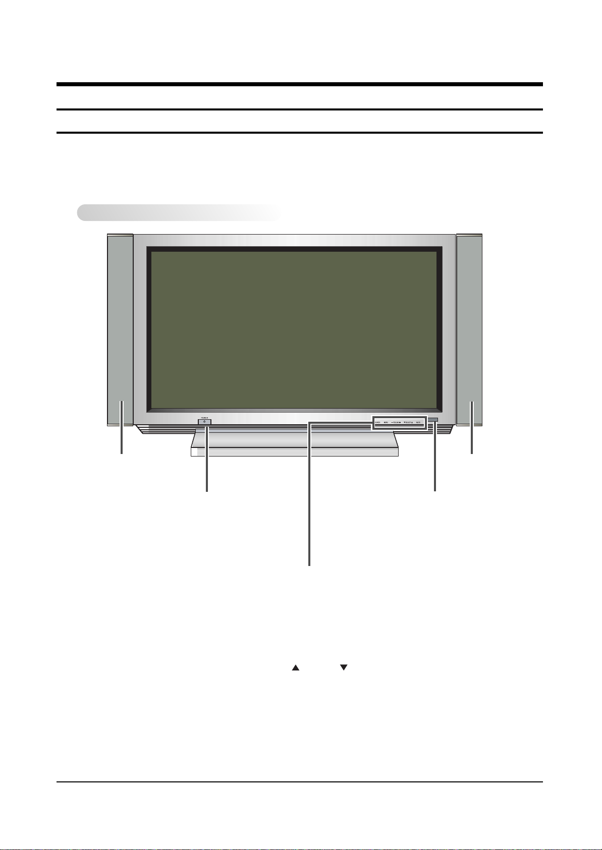
Handling Description
Samsung Electronics 9-1
9. Handling Description
9-1 Basic Description
9-1-1 The Name of Each Part
9-1-1(A) PDP(Plasma Disply Panel)
Front Panel
SPEAKER SPEAKER
POWER
Press to turn the
PDP on and off.
SOURCE
External input selection.
MENU
Menu display.
-
VOLUME +
Volume adjustment.
SELECT
Control the cursor in the Menu.
MUTE
Temporary sound switch-off.
Remote Control Signal Receiver
Aim the remote control towards this spot on
the PDP.
Page 99
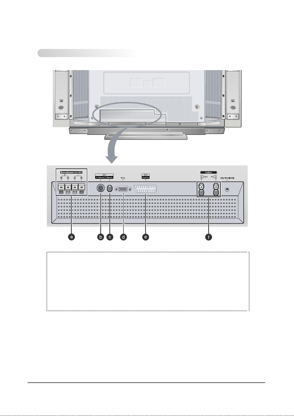
Handling Description
9-2 Samsung Electronics
Real Panel
a) External Speaker Outputs (8‰)
Connect external speakers.
b) S-VIDEO Input
Connect a S-Video signal from an S-VHS VCRs
or DVD players.
c) VIDEO Input
Connect a video signal from external sources
like VCRs or DVD players.
d) PC Input
Connect a PC signal from an PC.
e) SCART Audio/Video Input
Connect a audio/video signal from external
sources like VCRs.
f) Audio Inputs (Video/PC)
Connect a audio signal from external sources
like VCRs or PC.
Page 100
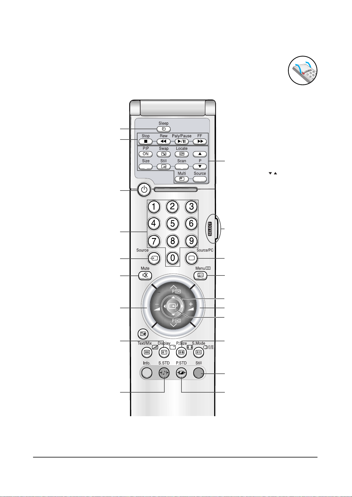
Handling Description
Samsung Electronics 9-3
9-1-1(B) REMOTE CONTROL
Filp the cover open in the arrow direction.
AUTOMATIC SWITCH-OFF
VCR/DVD FUNCTIONS;
(STOP/REWIND/PLAY/PAUSE/
FAST-FORWARD)
POWER ON/OFF
Power
PIP FUNCTIONS;
PIP ON/SWAP/LOCATE/
SIZE SETTING/STILL/SCAN/
CHANNEL SELECTION(P / )/
MULTI DISPLAY/
INPUT SOURCE SELECTION (SOURCE)
NUMERIC BUTTONS
EXTERNAL INPUT SELECTION
TEMPORARY SOUND SWITCH OFF
VOLUME DECREASE
DISPLAYING INFORMATIONS
SOUND EFFECT SELECTION
MAKE THE REMOTE CONTROL WORKS
FOR MONITOR, VCR, CABLE,
DVD PLAYER
SELECT TO THE PC MODE DIRECTLY
MENU DISPLAY
CONTROL THE CURSOR IN THE MENU
VOLUME INCREASE
CHANGE CONFIRMATION
PICTURE SIZE SELECTION
STILL THE MAIN PICTURE
PICTURE EFFECT SELECTION
 Loading...