


PS42D5SX/XEC
Table of contents
 Loading...
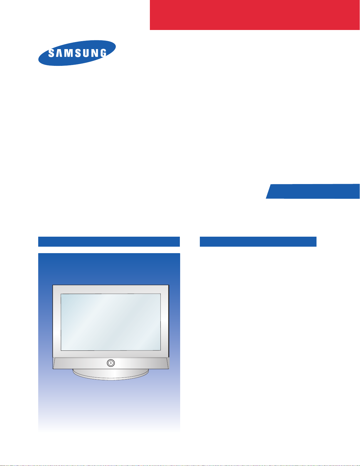
PLASMA DISPLAY TV
Chassis : D72A(P) Puccini_42D5
Model : PS42D5SX/XEC
PS42D5SX/XSG
PS42D5SX/XTL
PLASMA DISPLAY TV FEATURES
■■
DTV Ready PDP TV
■
2 Way 4 Speakers
■
■
1 HDMI input
■
Slim line design
■
■
Energy Saving
■
12 Bit image processing
(687 billion color)
SERVICE
Manual
42D5

Table of Contents
Chapter 1 Precaution
■ 1-1 Safety Precautions . . . . . . . . . . . . . . . . . . . . . . . . . . . . . . . . . . . . . . . . . . . . . . . . . . . . . . . . . . . 1-1
■ 1-2 Servicing Precautions . . . . . . . . . . . . . . . . . . . . . . . . . . . . . . . . . . . . . . . . . . . . . . . . . . . . . . . . 1-3
■ 1-3 Static Electricity Precautions . . . . . . . . . . . . . . . . . . . . . . . . . . . . . . . . . . . . . . . . . . . . . . . . . . . 1-4
■ 1-4 Installation Precautions . . . . . . . . . . . . . . . . . . . . . . . . . . . . . . . . . . . . . . . . . . . . . . . . . . . . . . . 1-5
Chapter 2 Product Specification
■ 2-1 Product Features . . . . . . . . . . . . . . . . . . . . . . . . . . . . . . . . . . . . . . . . . . . . . . . . . . . . . . . . . . . . 2-1
■ 2-2 Key Features . . . . . . . . . . . . . . . . . . . . . . . . . . . . . . . . . . . . . . . . . . . . . . . . . . . . . . . . . . . . . . . 2-2
■ 2-3 Specifications Analysis . . . . . . . . . . . . . . . . . . . . . . . . . . . . . . . . . . . . . . . . . . . . . . . . . . . . . . . . 2-5
■ 2-4 Accessories . . . . . . . . . . . . . . . . . . . . . . . . . . . . . . . . . . . . . . . . . . . . . . . . . . . . . . . . . . . . . . . . 2-6
Chapter 3 Alignment & Adjustment
■ 3-1 Service Instruction . . . . . . . . . . . . . . . . . . . . . . . . . . . . . . . . . . . . . . . . . . . . . . . . . . . . . . . . . . . 3-1
■ 3-2 How to Access Service Mode . . . . . . . . . . . . . . . . . . . . . . . . . . . . . . . . . . . . . . . . . . . . . . . . . . . 3-2
■ 3-3 Factory Data . . . . . . . . . . . . . . . . . . . . . . . . . . . . . . . . . . . . . . . . . . . . . . . . . . . . . . . . . . . . . . . . 3-3
■ 3-4 Service Adjustment . . . . . . . . . . . . . . . . . . . . . . . . . . . . . . . . . . . . . . . . . . . . . . . . . . . . . . . . . . 3-8
■ 3-5 Software Upgrade . . . . . . . . . . . . . . . . . . . . . . . . . . . . . . . . . . . . . . . . . . . . . . . . . . . . . . . . . . . 3-10
■ 3-6 Replacements & Calibration . . . . . . . . . . . . . . . . . . . . . . . . . . . . . . . . . . . . . . . . . . . . . . . . . . . . 3-14
Chapter 4 Exploded View & Part List
■ 4-1 PS42D5SX/XEC . . . . . . . . . . . . . . . . . . . . . . . . . . . . . . . . . . . . . . . . . . . . . . . . . . . . . . . . . . . . . 4-1
■ 4-2 PS42D5SX/XSG . . . . . . . . . . . . . . . . . . . . . . . . . . . . . . . . . . . . . . . . . . . . . . . . . . . . . . . . . . . . 4-2
■ 4-3 PS42D5SX/STL . . . . . . . . . . . . . . . . . . . . . . . . . . . . . . . . . . . . . . . . . . . . . . . . . . . . . . . . . . . . . 4-3
Chapter 5 Electrical Part List
■ 5-1 PS42D5SX/XEC . . . . . . . . . . . . . . . . . . . . . . . . . . . . . . . . . . . . . . . . . . . . . . . . . . . . . . . . . . . . . 5-1
■ 5-2 PS42D5SX/XSG . . . . . . . . . . . . . . . . . . . . . . . . . . . . . . . . . . . . . . . . . . . . . . . . . . . . . . . . . . . . 5-2
■ 5-3 PS42D5SX/STL . . . . . . . . . . . . . . . . . . . . . . . . . . . . . . . . . . . . . . . . . . . . . . . . . . . . . . . . . . . . . 5-3
Chapter 6 Troubleshooting
■ 6-1 First Checklist for Troubleshooting . . . . . . . . . . . . . . . . . . . . . . . . . . . . . . . . . . . . . . . . . . . . . . . 6-1
■ 6-2 Checkpoints by Error Mode . . . . . . . . . . . . . . . . . . . . . . . . . . . . . . . . . . . . . . . . . . . . . . . . . . . . 6-2
■ 6-3 Trouble-shooting with New Features . . . . . . . . . . . . . . . . . . . . . . . . . . . . . . . . . . . . . . . . . . . . . 6-6
■ 6-4 Troubleshooting Procedures by ASS'Y . . . . . . . . . . . . . . . . . . . . . . . . . . . . . . . . . . . . . . . . . . . 6-9
Chapter 7 Block Diagram
■ 7-1 Overall Block Diagram . . . . . . . . . . . . . . . . . . . . . . . . . . . . . . . . . . . . . . . . . . . . . . . . . . . . . . . . 7-1
■ 7-2 Partial Block Diagram . . . . . . . . . . . . . . . . . . . . . . . . . . . . . . . . . . . . . . . . . . . . . . . . . . . . . . . . . 7-2

Chapter 8 Wiring Diagram
■ 8-1 Overall Wiring . . . . . . . . . . . . . . . . . . . . . . . . . . . . . . . . . . . . . . . . . . . . . . . . . . . . . . . . . . . . . . . 8-1
■ 8-2 Partial Wiring . . . . . . . . . . . . . . . . . . . . . . . . . . . . . . . . . . . . . . . . . . . . . . . . . . . . . . . . . . . . . . . 8-2
Chapter 9 PCB Diagram
■ 9-1 PDP Module, SMPS . . . . . . . . . . . . . . . . . . . . . . . . . . . . . . . . . . . . . . . . . . . . . . . . . . . . . . . . . . 9-1
■ 9-2 Video Board, Function Key Borad, Power Button Board . . . . . . . . . . . . . . . . . . . . . . . . . . . . . . 9-4
Chapter 10 Schematic Diagram
■ 10-1 Main . . . . . . . . . . . . . . . . . . . . . . . . . . . . . . . . . . . . . . . . . . . . . . . . . . . . . . . . . . . . . . . . . . . . . 10-1
■ 10-2 Function . . . . . . . . . . . . . . . . . . . . . . . . . . . . . . . . . . . . . . . . . . . . . . . . . . . . . . . . . . . . . . . . . . 10-2
■ 10-3 Power/IR . . . . . . . . . . . . . . . . . . . . . . . . . . . . . . . . . . . . . . . . . . . . . . . . . . . . . . . . . . . . . . . . . 10-3
Chapter 11 Operation Instruction & Installation
■ 11-1 Product Features and Functions . . . . . . . . . . . . . . . . . . . . . . . . . . . . . . . . . . . . . . . . . . . . . . . 11-1
■ 11-2 New Features . . . . . . . . . . . . . . . . . . . . . . . . . . . . . . . . . . . . . . . . . . . . . . . . . . . . . . . . . . . . . . 11-6
■ 11-3 Installation Notes and Precautions . . . . . . . . . . . . . . . . . . . . . . . . . . . . . . . . . . . . . . . . . . . . . . 11-8
Chapter 12 Disassembly & Reassembly
■ 12-1 Overhaul Disassembly & Reassembly . . . . . . . . . . . . . . . . . . . . . . . . . . . . . . . . . . . . . . . . . . . 12-1
Chapter 13 Circuit Description
■ 13-1 Partial Block Descriptio . . . . . . . . . . . . . . . . . . . . . . . . . . . . . . . . . . . . . . . . . . . . . . . . . . . . . . 13-1
■ 13-2 New Circuit Description . . . . . . . . . . . . . . . . . . . . . . . . . . . . . . . . . . . . . . . . . . . . . . . . . . . . . . 13-25
Chapter 14 Reference Information
■ 14-1 Connection to a 3rd Party Device . . . . . . . . . . . . . . . . . . . . . . . . . . . . . . . . . . . . . . . . . . . . . . . 14-1
■ 14-2 Technical Terms . . . . . . . . . . . . . . . . . . . . . . . . . . . . . . . . . . . . . . . . . . . . . . . . . . . . . . . . . . . . 14-9

Alignment & Adjustment
Samsung Electronics 3-1
3. Alignment & Adjustment
3-1 Service Instruction
* Check items listed after changing each
1. Main Board replace : ATM Channel fixing and White Balance adjustment
2. Main SMPS Board replace: Vs, Va Voltage check and adjust
5. DC-DC SMPS Board replace : Output voltage check and adjust
6. Logic Board replace : Not adjustment
7 : Y-Main Board replace : Not adjustment
8 : X-Main Board replace : Not adjustment
9 : Buffer Board replace : Not adjustment
Alignment & Adjustment
3-2 Samsung Electronics
3-2 How to Access Service Mode
■ Using the Customer Remote
1. Turn the power off and set to stand-by mode.
2. Press the remote buttons in this order; POWER OFF-MUTE-1-8-2- POWER ON to turn the set on.
3. The set turns on and enters service mode.
4. Press the Power button to exit and store data in memory.
※ If you fail to enter service mode, repeat steps 1 and 2 above.
5. Initial SERVICE MODE DISPLAY State
※ The firmware version is subject to change without notice.
4. Buttons operations within Service Mode
Factory AIR 10
White Balance
uPD64083
ADV7402 Main
SDP51
MST9883
ADV7402 Sub
DNIe
Logic
PW318
Option
PW318 Upgrade
TL945 Upgrade
Reset
Release Date : XXX XX XXXX XX:XX:XX
Code No. : M1 Micom XX
PW318 T_XXXXXXXXX-XXXX
TL945 0.XX
Current input mode
Firmware version
MENU Full Menu Display / Move to Parent Menu
Direction keys ▲ / ▼
Item Selection by Moving the Cursor
Direction keys ◀ / ▶
Data Increase/Decrease for the Selected Item
Source Cycles through the active input source that are connected to the unit
Alignment & Adjustment
Samsung Electronics 3-3
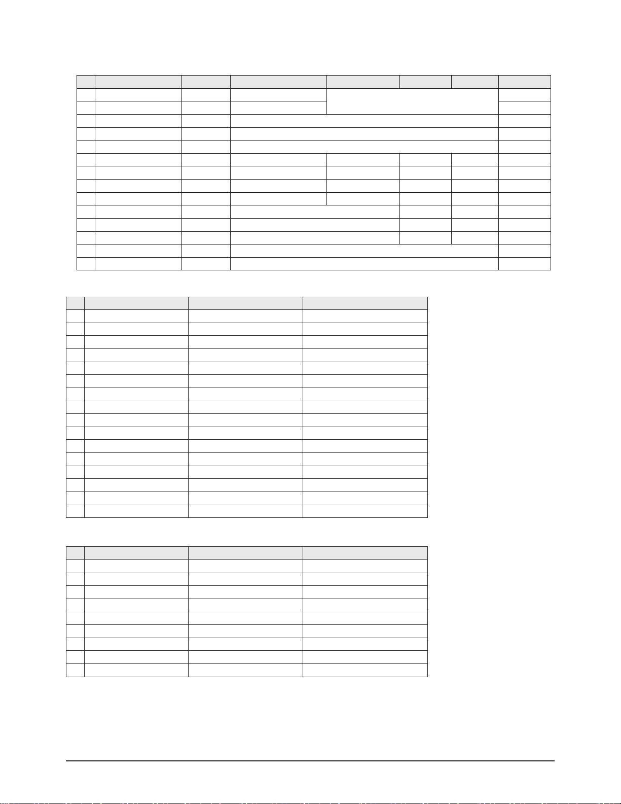
3-3 Factory Data
★ The underlined are items applied during the service adjustment. None of the others should be adjusted.
No ITEM Initial Value Remark
1 Panel Option 42S5S 42S5S/42D5S/42S5H
2 Gamma Mode - 2 Mode - 1,2,3,4
3 Analog Dimming Mode - 3 Mode - 1,2,3,4
4 Auto Power On ON/OFF
5 Key Lock OFF ON/OFF
6 Anynet OFF ON/OFF
7 DDC Write OFF ON/OFF
8 LNA ON ON/OFF
9 Ant. Gain Display OFF ON/OFF
10 Language English Osd language
11 Auto FM OFF ON/OFF
12 High Deviation Off ON/OFF
13 TTX On ON/OFF
14 TTX List Flop Flop/List
15 TTX TOP Off ON/OFF
16 TTX Group Auto Language TTX language
17 TTX Level Level 1.5 LEVEL 1.5 / 2.5
18 Shift Test OFF ON/OFF
19 Sound Delay1 OFF ON/OFF
20 Sound Delay2 OFF ON/OFF
21 Debug OFF ON/OFF
2. Option Table
1. Calibration
2. Option Table
3. White Balance
4. SVP-EX
5. SAA7119
6. MSP34XX/44XX
7. YC Delay
8. Adjust
9. DNIe
10. Chip Debugger OFF
11. Checksum
12. Reset
13. Spread Spectrum
14. Logic
T-PCN42PEUS-XXXX
SUB Micom Ver-xxxx
Fatory mode OSD Display
1. Calibration
① AV Calibration
② PC Calibration
③ DTV Calibration
Alignment & Adjustment
3-4 Samsung Electronics
No Item Range TV/AV Component PC DVI(HDMI)
1 Sub-Briteness 0~255 7 128 130 130
2 R-offset 0~255 138 128 138 138
3 G-offset 0~255 128 128 128 128
4 B-offset 0~255 146 128 144 144
5 Sub-Contrast 0~63 36 32 32 32
6 R-offset 0~255 128 128 128 128
7 G-offset 0~255 128 128 128 128
8 B-offset 0~255 148 128 128 128
3. White Balance
4. SVP-EX
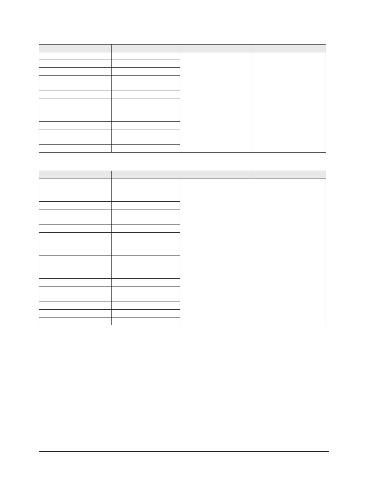
No Item Range Initial Value Remark
1 Y-Filter 0 ~ 255 80H
2 0 ~ 255 80H
3 0 ~ 255 80H
4 0 ~ 255 80H
5 0 ~ 255 80H
①ComB Filter
②Peaking
No Item Range Initial Value Remark
1 V-Peaking 0 ~ 255 80H
2 Peaking Delay 0 ~ 255 80H
3 Peaking Gain 0 ~ 255 80H
4 Peaking Width 0 ~ 255 80H
5 Praking f0 0 ~ 255 80H
③NR
No Item Range Initial Value Remark
1 Y-NR-Off 0 ~ 255 80H
2 C-NR-Off 0 ~ 255 80H
3 Y-NR-ON 0 ~ 255 80H
4 C-NR-ON 0 ~ 255 80H
④Deinterlace
No Item Range Initial Value Remark
1 Motion 0 ~ 255 80H
2 80H
3 80H
4 80H
Alignment & Adjustment
Samsung Electronics 3-5
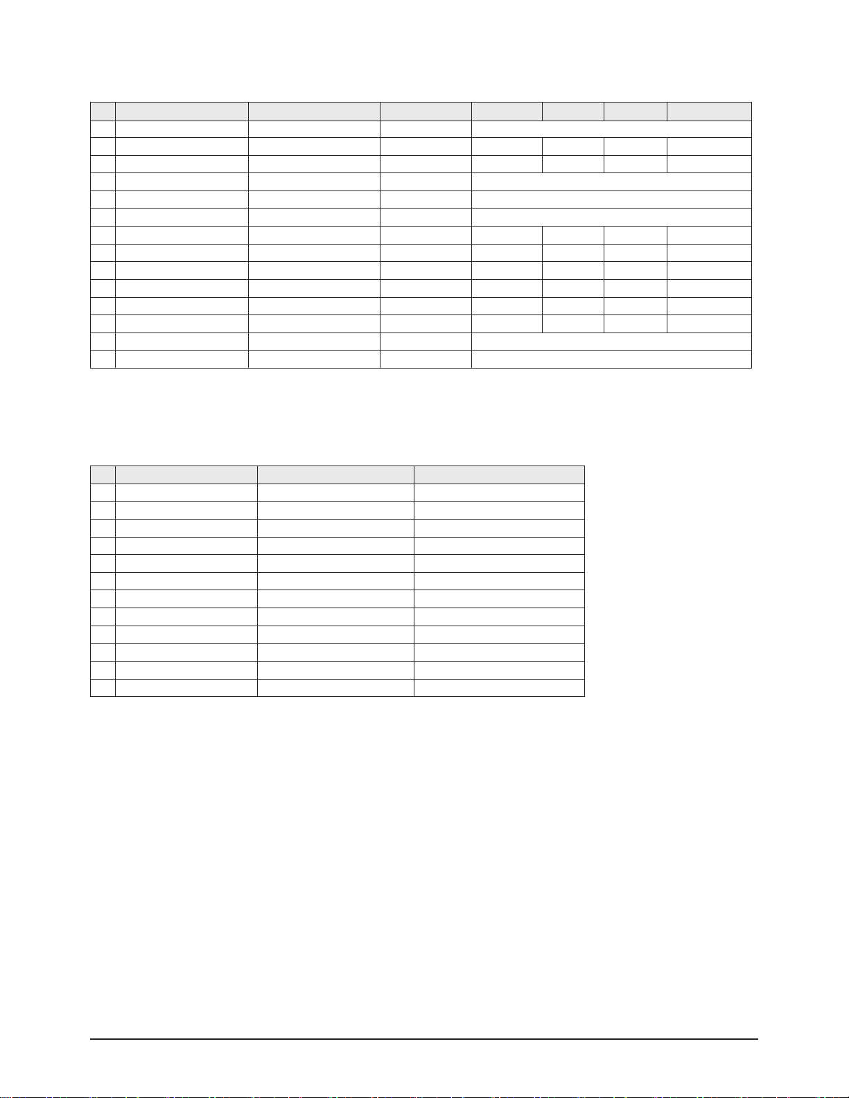
⑤Picture Gain Adjust
No Item Range TV/AV/S_Video Component PC DVI/HDMI
1 TCD3 Contrast 0 ~ 255 AV Calibration
78h
20h
2 TCD3 Brightness 0 ~ 255 AV Calibration
3 TCD3 CR Saturation 0 ~ 255 78h
4 TCD3 CB Saturation 0 ~ 255 78h
5 TCD3 YC Delay 0 ~ 15 00h
Range 480I/576I/480P/576P/1080I 720P PC HDMI
6 Analog Y/G offset 00 ~ 255 DTV Calibration PC Calibration 00 40h
7 Analog PB/B offset 00 ~ 255 DTV Calibration PC Calibration 02 00h
8 Analog PR/R offset 00 ~ 255 DTV Calibration PC Calibration 02 00h
9 Analog Y/G Gain 00 ~ 255 D6h E9h D6h
10 Analog PB/B Gain 00 ~ 255 FEh E9h FEh
11 Analog PR/R Gain 00 ~ 255 FEh E9h FEh
12 Black Level Setting 00 ~ 255 00h
13 Brightness(SVP) 0 ~ 255 00h
No Item Range Initial Value
1 HTC 00 ~ 255 2
2 ATVT 00 ~ 255 1
3 LUFI 00 ~ 255 5
4 NAICO_Brig 00 ~ 255 128
5 NAICO_Cont 00 ~ 255 64
6 NAICO_Satu 00 ~ 255 64
7 NAICO_Hue 00 ~ 255 3
8 COMP_Brig 00 ~ 255 162
9 COMP_Cont 00 ~ 255 92
10 COMP_Satu 00 ~ 255 64
11 TASKA_Brig 00 ~ 255 140
12 TASKA_Cont 00 ~ 255 64
13 TASKA_Satu 00 ~ 255 64
14 LIMOD 00 ~ 255 0
15 LIFIL 00 ~ 255 2
16 LIWGT 00 ~ 255 3
5. SAA7119
No Item Range Initial Value
1 FM-Prescale 00 ~ 255 20h
2 NT-M-Prescale 00 ~ 255 20h
3 SECAM-L-Prescale 00 ~ 255 22h
4 AV-Prescale 00 ~ 255 1Ah
5 I2S_1 Prescale 00 ~ 255 10h
6 I2S_2 Prescale 00 ~ 255 10h
7 Carrier Mute 00 ~ 255 42h
8 Pilot High 00 ~ 255 0Eh
9 Pilot Low 00 ~ 255 07h
6. MSP34XX/44XX
Alignment & Adjustment
3-6 Samsung Electronics
7. YC Delay
No Item Range TV/AV/S_Video Component PC DVI/HDMI Remark
1 RF PAL-B/G 00 ~ 255 102
77h 77h 77h
-
2 RF PAL-D/K 00 ~ 255 136
3 RF PAL- I 00 ~ 255 102
4 RF SECAM-B/G 00 ~ 255 51
5 RF SECAM-D/K 00 ~ 255 34
6 RF SECAM-L/L' 00 ~ 255 51
7 RF NTSC3.58 00 ~ 255 187
8 RF NTSC4.43 00 ~ 255 187
9 AV PAL 00 ~ 255 67
10 AV SECAM 00 ~ 255 34
11 AV NTSC 3.58 00 ~ 255 102
12 AV NTSC4.43 00 ~ 255 102
13 AV PAL60 00 ~ 255 119
8. Adjust
No Item Range TV/AV/S_Video Component PC DVI/HDMI Remark
1 Video Mute Time 10
-
2 Melody Volume 0 ~ 20 5
3 TTX Contrast 0 ~ 100 50
4 TTX Brightness 0 ~ 100 50
5 TTX Color 0 ~ 100 50
6 Dynamic Contrast 0 ~ 100 100
7 Dynamic Color 0 ~ 100 50
8 Dynamic Sharpness 0 ~ 100 60
9 Standard Contrast 0 ~ 100 90
10 Standard Brightness 0 ~ 100 80
11 Standard Color 0 ~ 100 70
12 Standard Sharpness 0 ~ 100 70
13 Movie Contrast 0 ~ 100 60
14 Movie Brightness 0 ~ 100 50
15 Movie Color 0 ~ 100 50
16 Movie Sharpness 0 ~ 100 40
17 RF_dB_1 0 ~ 255 0
18 RF_dB_2 0 ~ 255 0
19 RF_dB_3 0 ~ 255 0
Alignment & Adjustment
Samsung Electronics 3-7
9. DNIe Lite
No Item Range TV/AV/S_Video TV/AV/S_Video Component PC DVI/HDMI
1 PATT_SEL DNIe Lite 0x002C [13:08] 0 ~ 63 0
2 BLACK_TILT DNIe Lite 0x005E [15:08] 00 ~ 255 120 120 80 120
3 BLACK_GAINMAX DNIe Lite 0x00B9 [09:00] 00 ~ 1023 85 85 93 95
4 TEST_MCC DNIe Lite 0x00C1 [12] 0 ~ 1 0
5 OVERLAP_MCM DNIe Lite 0x00C1 [11:10] 00 ~ 03 0
6 AREA_EN_MCC DNIe Lite 0x0062 [15:11] 00 ~ 31 31
7 R-Offset(Post) DNIe Lite 0x0080 [09:00] -512 ~ 511 0 0 0 0
8 G-Offset(Post) DNIe Lite 0x0081 [09:00] -512 ~ 511 0 0 0 0
9 B-Offset(Post) DNIe Lite 0x0082 [09:00] -512 ~ 511 0 0 0 0
10 R-Gain(Post) DNIe Lite 0x007B [07 : 00] 0 ~ 255 128 128 128 128
11 G-Gain(Post) DNIe Lite 0x007C [15 : 08] 0 ~ 255 128 128 128 128
12 B-Gain(Post) DNIe Lite 0x007C [07 : 00] 0 ~ 255 128 128 128 128
13 Com_Offset_Sel(Post) DNIe Lite 0x00F2 [13] 0 , 1 1
14 Com_Gain_Sel(Post) DNIe Lite 0x00F2 [14] 0 , 1 1
10. Chip Debugger : ON/OFF
11. Checksum XXXX XXXX
12. Reset
13. Spread Spectrum
14. Logic
No Item Range Initial Value
1 Int/Ext Sel 0
2 Pat Sel 0
3 FCRL CON 0
4 Image Sticking 0
5 Error Mode Check 0
6 Error Code Table 0
7 Vs Reference 0
8 Vs Average 0
9 Vs to D/A 0
10 Va Reference 0
11 Va Average 0
12 Va to D/A 0
Alignment & Adjustment
3-8 Samsung Electronics
3-4 Service Adjustment
3-4-1 White Balance Adjustment
1. W/B Adjustment is required for the following two modes : : Component → Video
(Signal equipment : MSPG-925LTH, Measurement equipment : CA210)
※ To adjust HDMI, use the HDMI ↔ DVI conversion cable, and connect the DVI output from MSPG-925LTH to the HDMI input.
2. Adjustment Method
-Component and Video mode Adjustment PC, HDMI mode offset.
※ Thus, Micom saves the PS42S5S W/B data separately for each memory mode of the block
- White Balance Coordinates by Mode
VIDEO COMPONENT
H/L
(High Light)
x 265 265
y 265 265
Y(fL) 31 21
L/L
Low Light
x 280 280
y 285 285
Y(fL) 1.3 0.8
1. Pattern Generator Device: 925 LTH (Manufacturer: Master)
2. Adjust Pattern : ABL Pattern(Master 925LTH #16 Pattern)
3. Adjust Timing : Video - PAL(Master 925LTH Model #2)
Component - 720P(Master 925LTH Model # 6)
4. The adjustment procedures for each mode are described as follows:
1) Component
① Send the Toshiba ABL Pattern (Pattern #16) of the 1080i (Model #5) resolution signal to theComponent in port using
the Master 925 LTH.
② Enter Factory mode, move to "White Balance" and click Select.
③ Set the coordinates of H/Land L/L by adjusting "Sub Contrast", "Sub Bright", "R Drive", "G Drive", "B Drive", "R Cutoff"
, "G Cutoff" , and "B Cutoff".
2) Video
① Send the Toshiba ABL Pattern (Pattern #16) of the 1080i (Model #5) resolution signal to the Video in port using the
Master 925 LTH.
② Enter Factory mode, move to "White Balance" and click Select.
③ Set the coordinates of H/Land L/L by adjusting "Sub Contrast", "Sub Bright", "R Drive", "G Drive", "B Drive", "R Cutoff"
, "G Cutoff" , and "B Cutoff".
Alignment & Adjustment
Samsung Electronics 3-9
H/L Point
L/L Point
Alignment & Adjustment
3-10 Samsung Electronics
3-5 Software Upgrade
3-5-1 Digital Board TL945 Flash Upgrade
1. Connect one end of the RS-232C cable to the PC COM port and the other end of the cable to the PDP Service port while the
power of the PDP is off.
2. Rome Flash Downloader.

Alignment & Adjustment
Samsung Electronics 3-11
3. When the Flash Downloader is launched, click the Open button.
4. Select a file to be downloaded from the computer.

Alignment & Adjustment
3-12 Samsung Electronics
5. After selecting a target file, click the Connect button and turn the power on. When the program is activated, Ready click.
6. Note that the power must not be turned off during the download.

Alignment & Adjustment
Samsung Electronics 3-13
7. After the download is finished, the Flash Download Completed popup window opens. That indicates S/W upgrade is completed.

Alignment & Adjustment
3-14 Samsung Electronics
3-6 Replacements & Calibration
3-6-1 Voltage Adjustment
※ When the SMPS is replaced, the Va, Vs voltages must be checked and adjusted to the proper levels indicated on the panel
sticker.
adjustment
adjustment
Voltage Label
adjustment
Vscan
Vset
Ve
VR514 Va
adjustment
VR432 Vs
adjustment
Block Diagram
Samsung Electronics 7-1
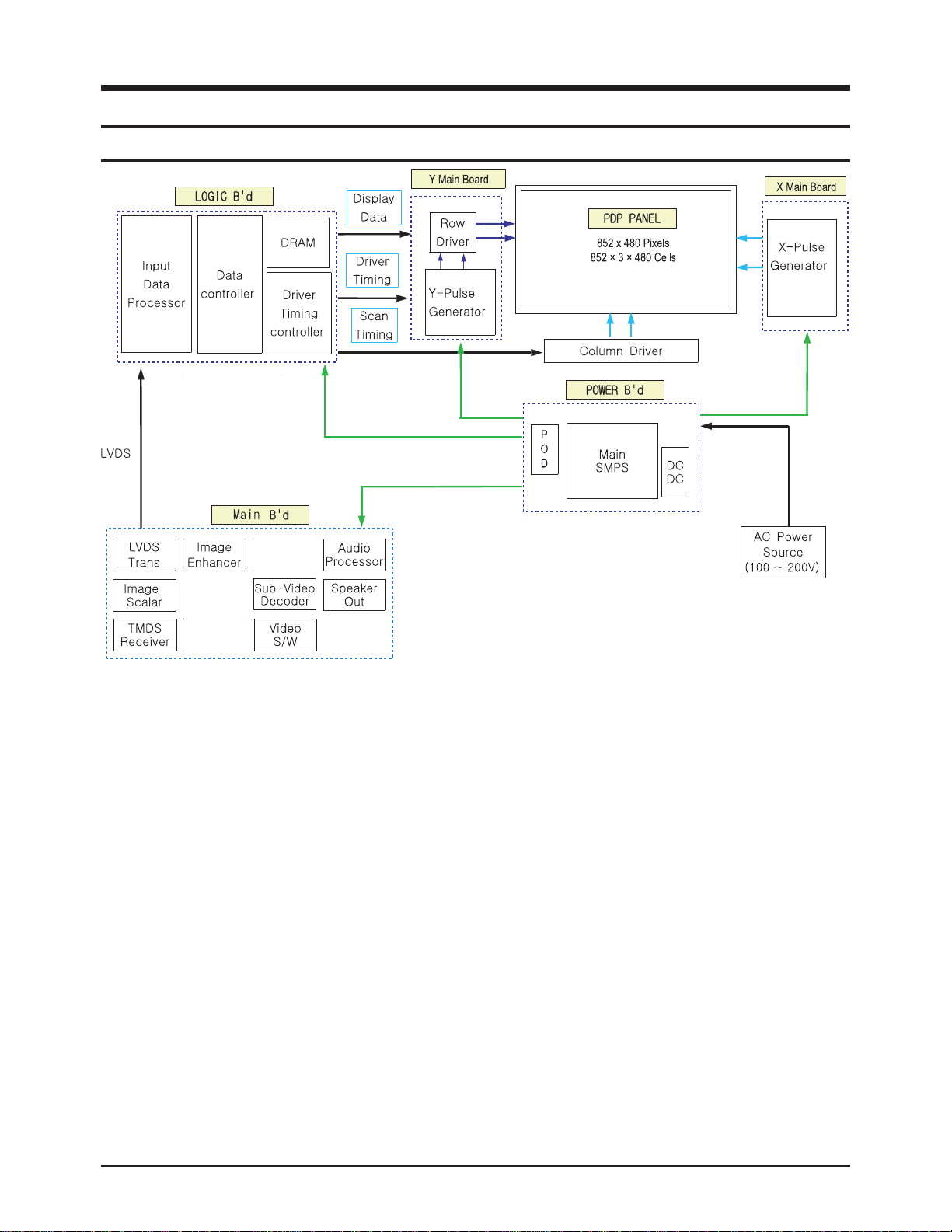
7. Block Diagram
7-1 Overall Block Diagram
Block Diagram
7-2 Samsung Electronics
7-2 Partial Block Diagram
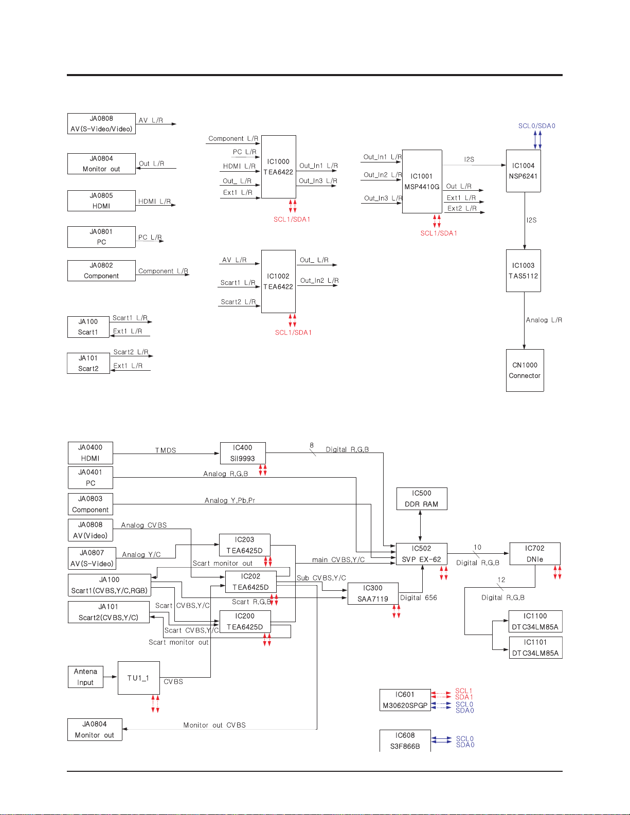
7-2-1 Audio Signal Block Diagram
7-2-2 Video Signal Block Diagram
Block Diagram
Samsung Electronics 7-3
7-2-3 Logic Board Block Diagram

7-4 Samsung Electronics
MEMO
Circuit Description
Samsung Electronics 13-1
13. Circuit Description
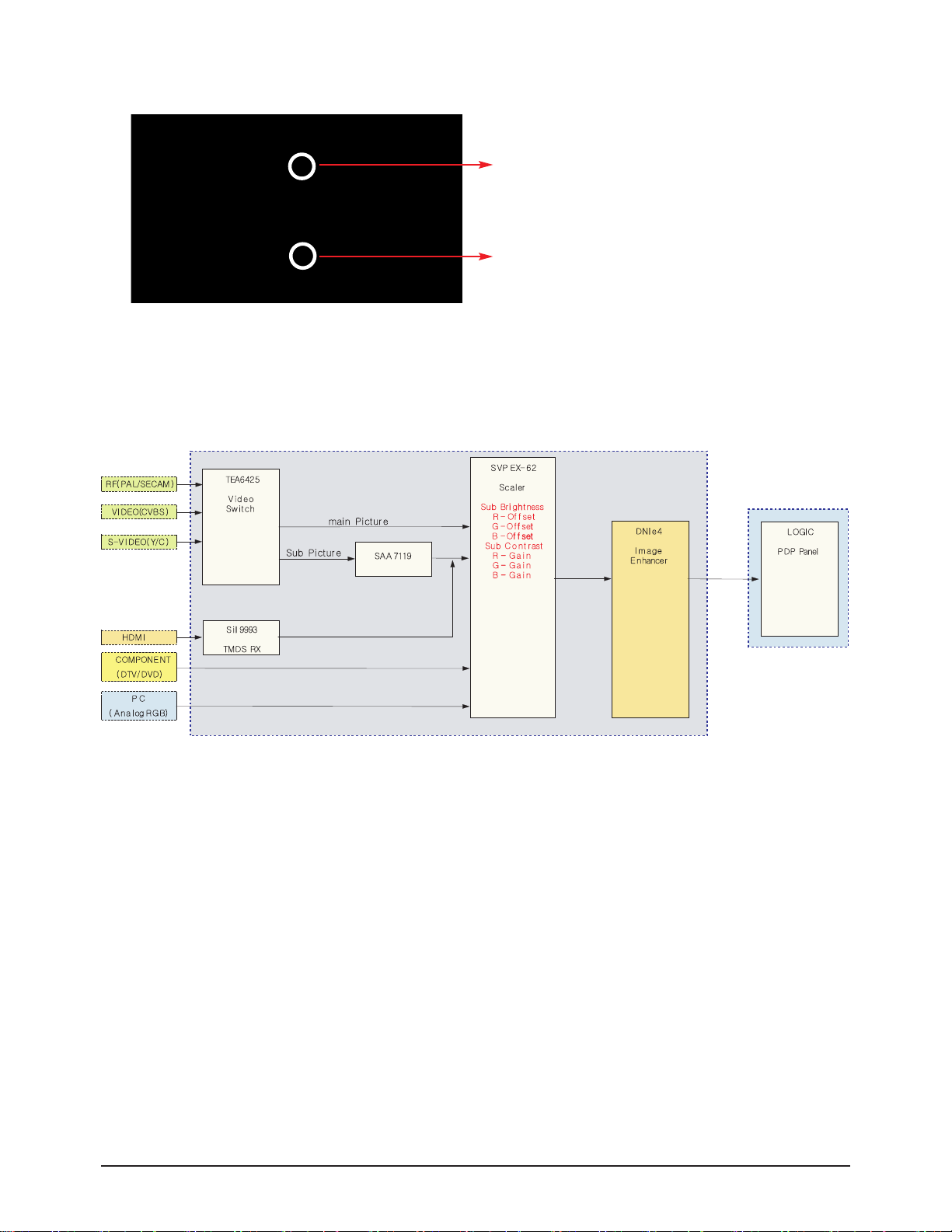
13-1 Partial Block Description
13-1-1 Main Board
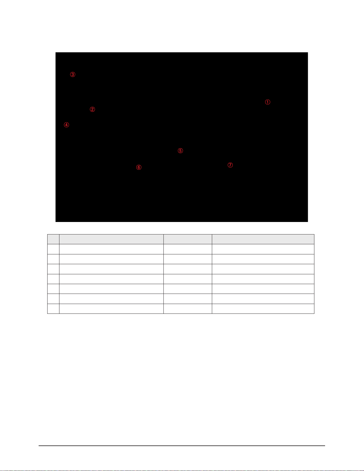
No Name Function Description
①
SVP-EX62 main Video Decorder+Deinterlacer+Scaler
AScaler IC that generates the output resolution appropriate to the PDP panel and
generates the PIP screen.
②
DNIe-L Image Enhancer The DNIe IC for visual quality improvement.
③
M30620SPGP main Micom Generates various control signals required for operating the circuit.
④
SAA7119 sub Video Decorder
The Video Decoder IC that converts the Y/C and Scart RGB signals for the main
screen into 10 bit digita R, G, B signals.
⑤
SIL9993 HDMI Decorder Converts the TMDS signal on the HDMI input into 8 bit digital R, G, B signals
⑥
S3F8668 sub Micom
Detects the Power on/off signal from the remote control and the Power button and
turns SMPS on or off, handles the Caption signal, and controls the signal for the
LEDs on the front panel.
⑦
MSP4410G Sound processor Sound Processing IC
⑧
NSP6241 Sound Effect chip Sound PWM IC
⑨
TMQZ6-405A Tuner Tuner CH Tuning and CVBS, SIF
Circuit Description
13-2 Samsung Electronics
13-1-2 Power Button Board
(1) RM01: Remote Control Sensor.
(2) SW001: Power button
(3) OP001: The Illumination sensor that senses the quantity
of light. It senses the illumination and automati
cally adjusts the screen brightness according to
the surrounding brightness when the Power
Saving Mode of the User menu is set to Auto.
13-1-3 Function Key Board
Function Key. Located on the side of the unit.
Circuit Description
Samsung Electronics 13-3
(1) CN800: AC IN (90 ~ 264V)
※ CN811, CN806, CN807 and CN808 are not used.
13-2-4 Main SMPS
(2)
CN804-2
(MAIN SMPS)
↔
CN109(READY B'D)
Pin No Signal
1 ■
FAN-D
2 FAN-ON
3 STB5V
4 RTN
5 PS-ON
6 12V
7 RTN
8 RTN
9 VCA
10 VCS
11 RTN
12 5.3V
13 RTN
14 5.3V
(3)
CN803(MAIN SMPS)
↔
CN108(READY B'D)
Pin No Signal
1 ■
RTN
2 VT(33V)
3 RTN_AMP
4 RTN_AMP
5 18V_AMP
6 18V_AMP
7 RTN
8 12V
9 RTN
10 6V
(4)
CN810(Main SMPS)
↔
CN2013(Logic B'D)
Pin No Signal
1 ■
5.3V
2 5.3V
3 RTN
4 RTN
5 5.3V
6 RTN
7 PS-ON
8 N.C
9 VS-ON
10 STB 5V
(5)
CN809(Main SMPS)
↔
CN3(DC-DC SMPS)
Pin No Signal
1 ■
5.3V
2 Vg
3 RTN
4 RTN
5 RTN
6 RTN
7 RTN
8 Va
9 Va
10 N.C
11 Vs
12 Vs
Circuit Description
13-4 Samsung Electronics
1. Outline (PDP 42inch/50inch SMPS)
Considering various related conditions, the switching regulator with good efficiency and allowing for its small size and light weight
was used as the power supply for PDP 42inch(Schubert)/50inch(Strauss), VS requiring high power consumption Asymmetrical Half
Bridge converter and flyback converter. To comply with the international harmonics standards and improve the power factor, active
PFC(Power Factor Correction) was used to rectify AC input into +400V DC output, which in turns used as input to the switching
regulator.
2. Input
The power supply shall be capable of supplying full rated output power over free voltage ranges that are rated 100 VAC - 240 VAC
RMS nominal. Operating voltage : 90 VAC - 264 VAC
The power supply must be able to start up under peak loading at 90V AC. The power supply shall automatically recover from AC
power loss. (Note that nominal voltages for test purposes are considered to be with +/- 1.0V of nominal).
STD_5V & Vpr2(3.3V) is a SELV standby voltage that is always present when AC mains voltage present.
3. Output
4. Over Voltage Protection
The over voltage sense circuitry and reference shall reside in package that are separate and distinct from the regulator control
circuitry and reference. No single point fault shall be able to cause a sustained over voltage condition on any of all outputs.
The supply shall provide latch-mode Over Voltage Protection as defined below.
5. Short Circuit and Over current Protection
An output short circuit is defined as output impedance of less than 300mohms. The power supply shall shutdown and latch off for
shorting VS DC rails to return. Shorts between main output rails and STD_5V shall not cause any damages to the power supply.
The power supply shall either shutdown and latch off for shorting is removed, the P/S shall recover. The power supply shall be
capable of withstanding a continuous short-circuit to the output without damage or over stress to the unit (components, PCB
traces,connectors,etc.) under the input conditions specified in Section 3 above. Current Protection as defined below.
Output Name Output Voltage Output Current(Max.) Using in PDP Driving
VS +190V ~ 220V (210V) 2.0A Sustain Voltage of Drive Board
VA +60V ~ 80V (70V) 3.0A Address Voltage of Drive Board
D5.3V +5.3V 5.0A
A6.5V +6.5V 3.0A
FAN_9V +9V 0.2A
VG +15V 1.0A
D12V +12V 1.5A
A12V +5.3V 0.5A
18VAMP +18V 2.5A Amp Voltage of Audio Board
VT +33V 0.006A
STD_5V +5V 1.0A Standby for Remote Control
Parameter Min Unit
VS(210V) 250 ~ V
VA(70V) 100 ~ V
VCC(+5.3V) 6.8 ~ V
Output Over Current Limit Unit
VS(210V) 20A, Constant Current.(TBD) A
VA(70V) 10A, Constant Current.(TBD) A
Output except Vs,Va No damage (Auto Recovery or Shut down.) A
Circuit Description
Samsung Electronics 13-5
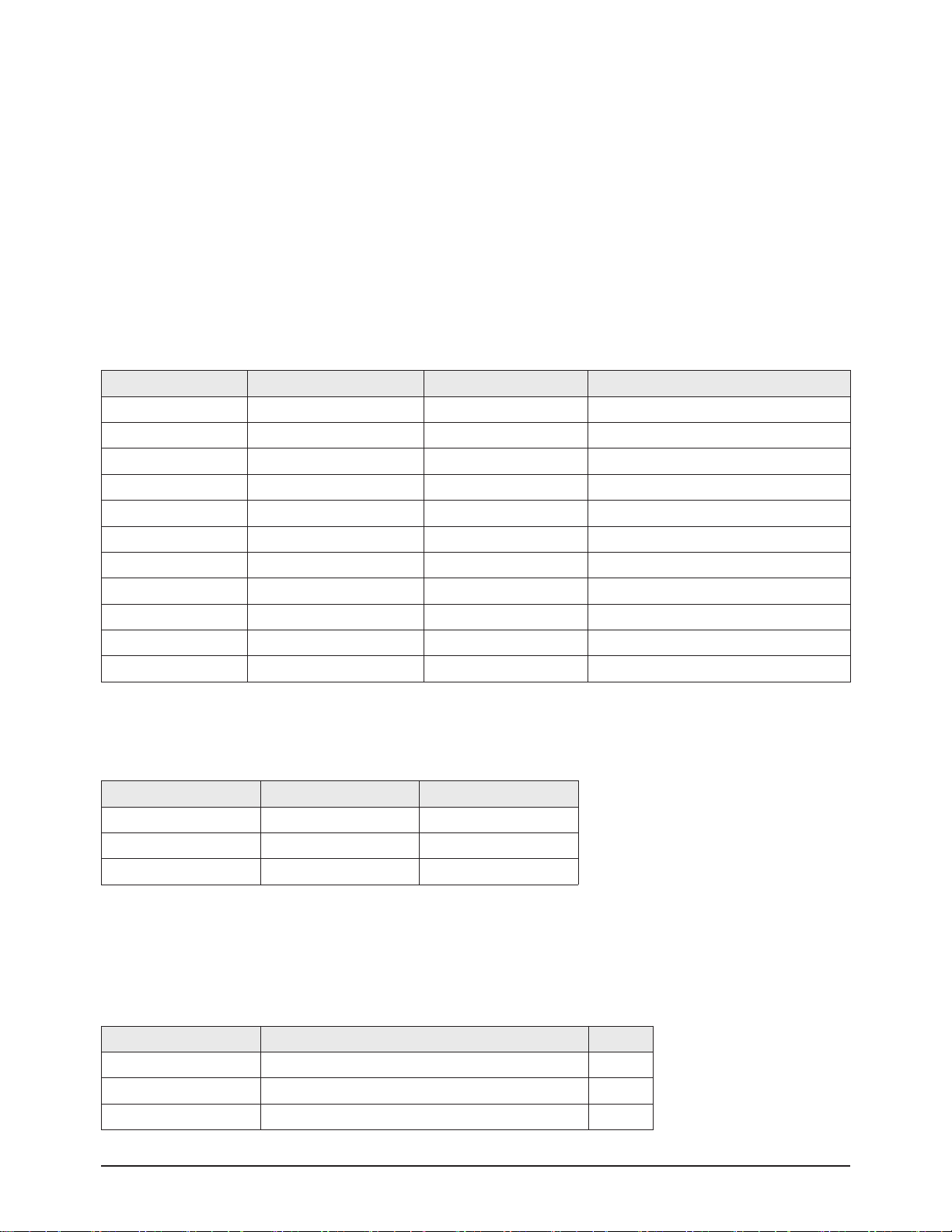
6. Troubleshooting
Normal
Power ON
STD_5V
Abnormal
Check the U101, D108
VA
Normal
Normal
PFC
Abnormal
VS
Abnormal
Abnormal
Multi
Check the Q401, Q402
Check the U201, Q203, Q204
Check the U501
Abnormal
Check the U601
Normal
Check the Other board (Image Board or Driver Board) or Cable.
Circuit Description
13-6 Samsung Electronics
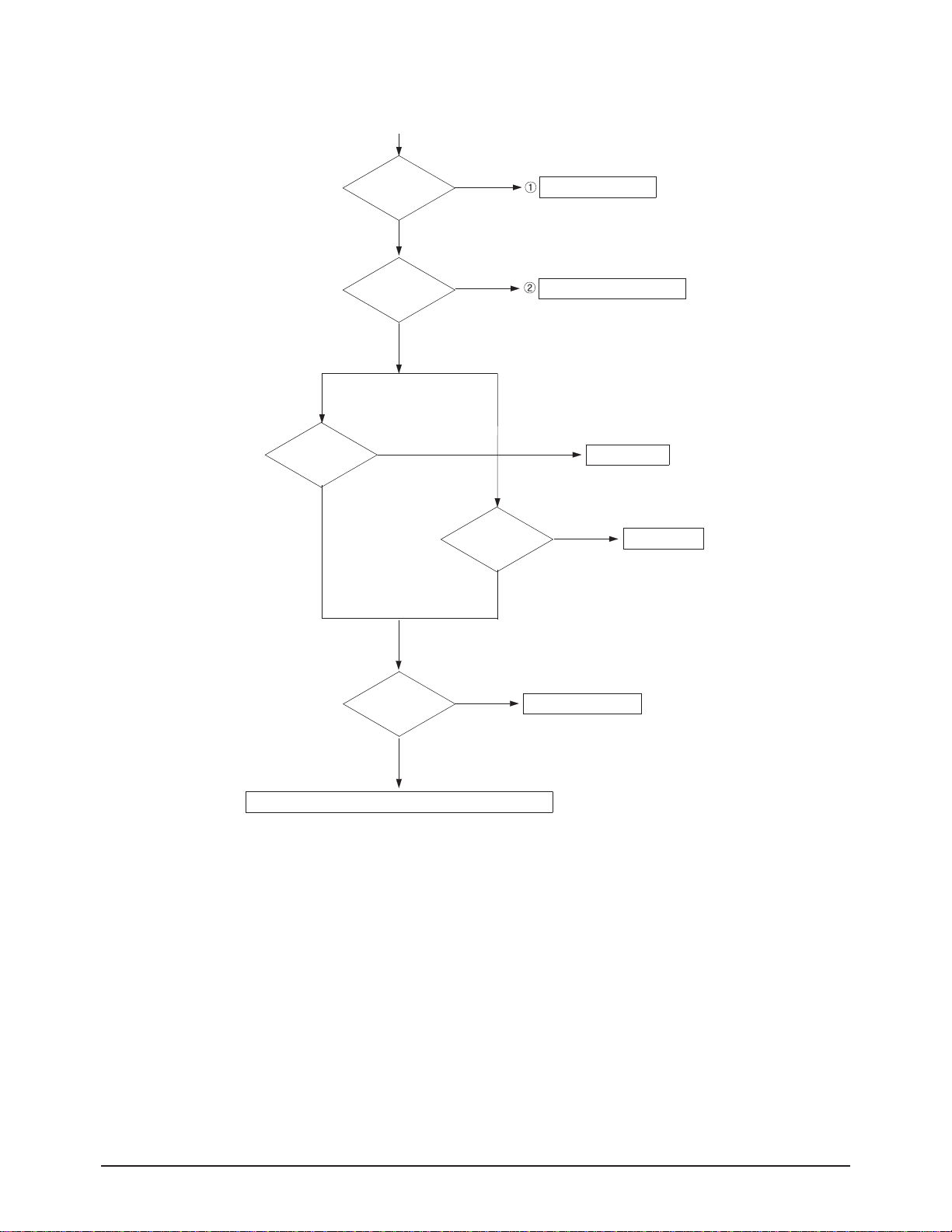
(6) D5.3V, Vg, Ve Test Point
(7) Va, Vset, Vscan Test Point
13-1-5 DC-DC SMPS
(1)
CN809(Main SMPS)
↔
CN3(DC-DC SMPS)
Pin No Signal
1 ■
5.3V
2 Vg
3 RTN
4 RTN
5 RTN
6 RTN
7 RTN
8 Va
9 Va
10 N.C
11 Vs
12 Vs
(4), (5)
CN1, CN6
(DC-DC SMPS)
↔
CN2501(E-Buffer),
CN2701(G-Buffer)
Pin No Signal
1 ■
RTN
2 N.C
3 5.3V
4 N.C
5 Va
(2)
CN2(DC-DC SMPS)
↔ CN5007(YB'D)
Pin No Signal
1 ■
Vs
2 Vs
3 RTN
4 RTN
5 Vset
6 RTN
7 Vscan
8 RTN
9 Vg
10 5.3V
(3)
CN4(DC-DC SMPS)
↔ CN4000(X B'D)
Pin No Signal
1 ■
Vs
2 Vs
3 RTN
4 RTN
5 Ve
6 RTN
7 RTN
8 Vg
9 5.3V
Circuit Description
Samsung Electronics 13-7
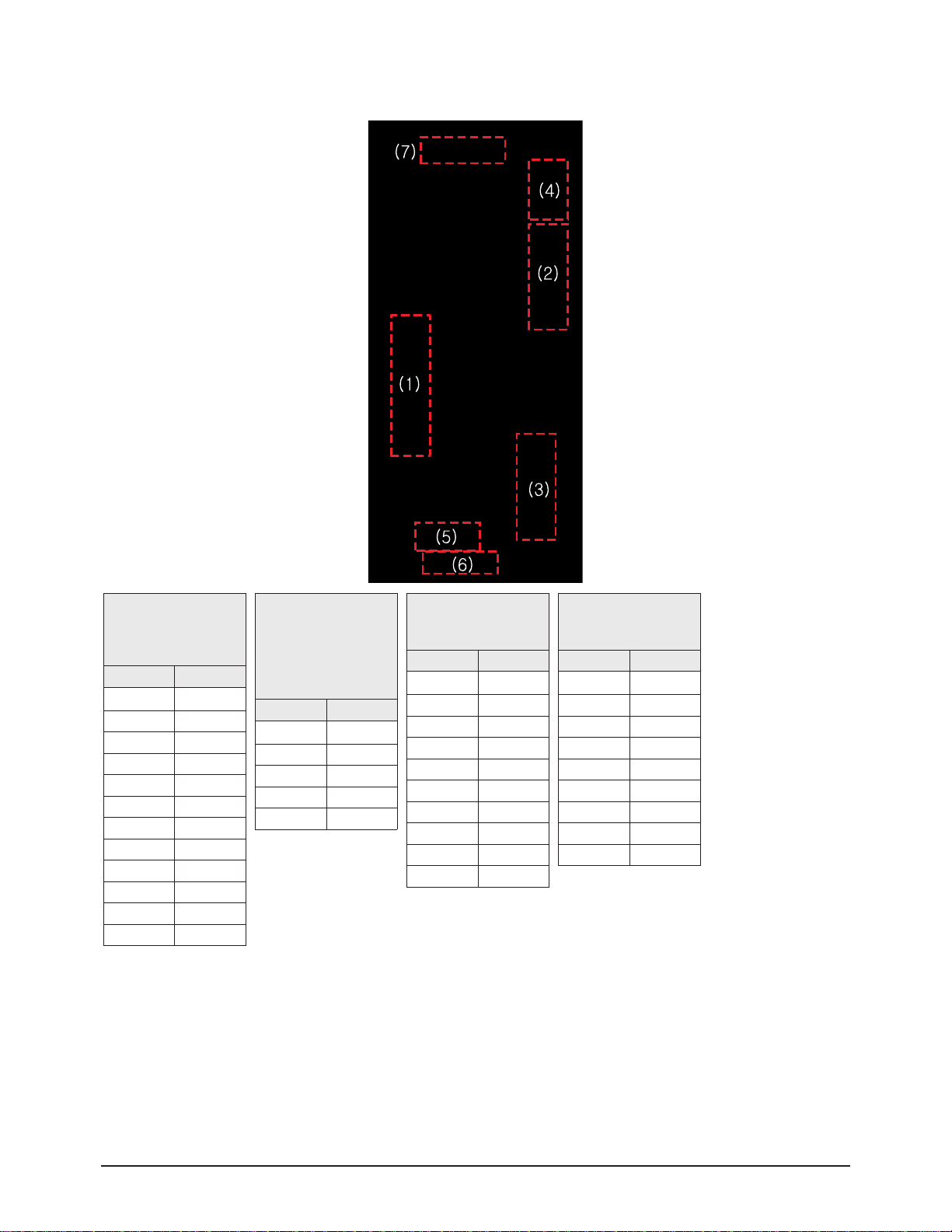
DC DC SMPS receives Vs input (195~215V) from the Main SMPS and the necessary Vscan, Vset and Ve voltages are output to
operate the PDP Module as shown in the block diagram above.
1. Block Diagram
Vs Input Part Vscan Output
Transformer
Control
and
Switching Block
Control
and
Switching Block
Control
and
Switching Block
Auxiliary
Power
Transformer
Auxiliary
Power
Transformer
Auxiliary
Power
Rectification
Block
Feedback
Block
Rectification
Block
Feedback
Block
Rectification
Block
Feedback
Block
Vset Output
Ve Output
Circuit Description
13-8 Samsung Electronics
13-1-6 PDP Module
No Name Parts Code Description
1 ASSY PDPP-X MAIN BOARD BN96-02038A X Drive Board
2 ASSY PDP P-Y MAIN BOARD BN96-02039A Y Drive Board
3 ASSY PDP P-Y BUFF UPPER BOARD BN96-02040A Y Buffer Upper Board
4 ASSY PDP P-Y BUFF LOWER BOARD BN96-02041A Y Buffer Lower Board
5 ASSY PDP P-LOGIC BOARD BN96-02042A Logic Board
6 ASSY PDP P-ADDRESS E BUFF BOARD BN96-02043A Address E Buffer Board
7 ASSY PDP P-ADDRESS F BUFF BOARD BN96-02044A Address f Buffer Board
Circuit Description
Samsung Electronics 13-9
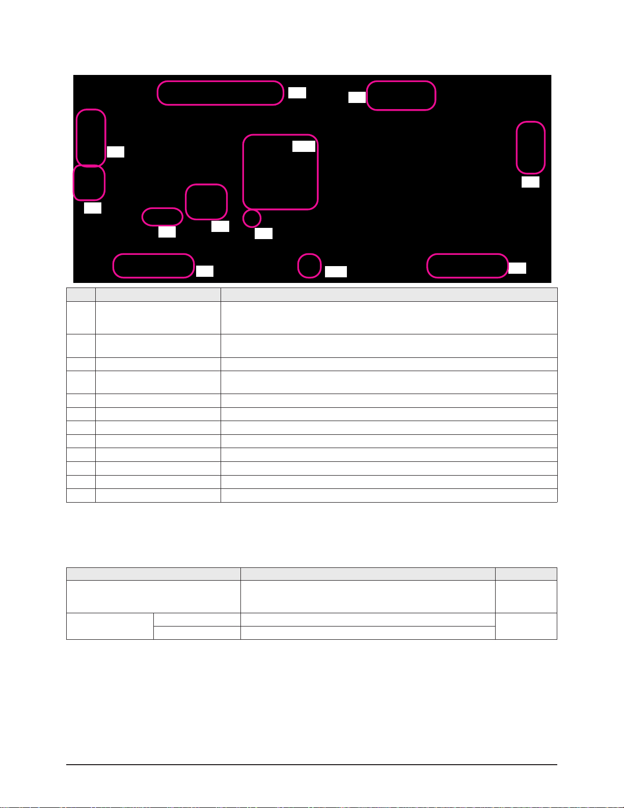
■ A name of main part of Logic Board and vocabulary.
Item Name Explanation
①
LVDS Connector
The connector to receive the RGB, H, V, DATAEN and DCLK signals that have been LVDS encoded through the
video board. At present, there are 2 LVDS, both internal and external, and only LVDS will be provided in the final
version of the board.
②
Operating Status LED
The LED that shows whether the Sync and Clock signal is properly supplied to the logic board (Normal Status:
Blinks at 0.8 second intervals)
③
I2C Connector The connector for the Key Scan board that checks and controls the 512K data.
④
MICOM(ARM-PROCESSOR)
512K including the Gamma Table, APC Table, drive waveform timing and other options is saved to internal flash
memory.
⑤
Y Connector The connector to output the control signal for the Y drive board.
⑥
X Connector The connector to output the control signal for the X drive board.
⑦
CN2075(E-Adderss Buffer Connector) The connector to output the address data and the control signal to the E-buffer board.
⑧
CN2076(F-Adderss Buffer Connector) The connector to output the address data and the control signal to the F-buffer board.
⑨
Power Connector The connector to receive power (5V, 3.3V) for the Logic board.
⑩
ASIC CHIP The main processor that generates and outputs the logic drive signal and the address data.
⑪
MICOM LOADING 5PIN CONNECTOR The connector to load the Micom drive program. The program is loaded by connecting to the GA-WRITER.
⑫
VTOGG TP for V Sync Check
■ About Logic Board
The Logic Board consists of a Logic Main board, which processes the video signal input through LVDS and creates the address
driver output and XY drive signals, and a Buffer board, which buffers the output signal and outputs the signal to the Address Driver
IC (TCP IC).
Logic Board Function Remark
Logic Main
- Video Signal Processing (W/L, error diffusion, APC)
- Outputs the Address Driver Control and Data Signals to the Buffer board.
- Outputs the XY Drive Board Control Signal
Buffer Board
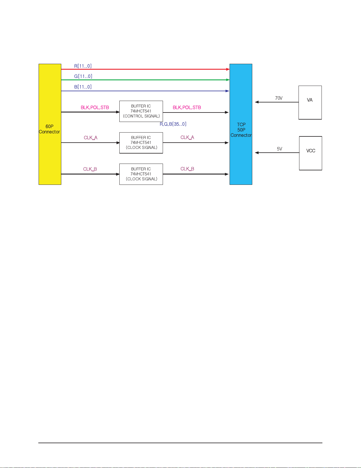
E Buffer Board Outputs data and control signals to the bottom left TCP IC.
F Buffer Board Outputs data and control signals to the bottom right TCP IC.
1
5
01
9
3
11
4
7
2
21
6
8
Loading...