


PLASMA DISPLAY TV
Chassis : D53A(P)_42”_SetTop
Model: PS42P2SBX/XEC
PS42P2SBX/XEH
PS42P2SBX/XEU
PS42PNSBX/XEC
|
|
PLASMA DIAPLAY TV |
|
|
|
C O N T E N T S |
|||||||||
|
|
|
|
|
|
|
|
|
|
|
1. |
Precautions |
|||
|
|
|
|
|
|
|
|
|
|
|
|
|
|||
|
|
|
|
|
|
|
|
|
|
|
|
|
|||
|
|
|
|
|
|
|
|
|
|
|
|
|
2. |
Reference Information |
|
|
|
|
|
|
|
|
|
|
|
|
|
|
|||
|
|
|
|
|
|
|
|
|
|
|
|
|
|||
|
|
|
|
|
|
|
|
|
|
|
|
|
|||
|
|
|
|
|
|
|
|
|
|
|
|
|
|||
|
|
|
|
|
|
|
|
|
|
|
|
|
3. |
Specifications |
|
|
|
|
|
|
|
|
|
|
|
|
|
|
|||
|
|
|
|
|
|
|
|
|
|
|
|
|
|||
|
|
|
|
|
|
|
|
|
|
|
|
|
|||
|
|
|
|
|
|
|
|
|
|
|
|
|
|||
|
|
|
|
|
|
|
|
|
|
|
|
|
|||
|
|
|
|
|
|
|
|
|
|
|
|
|
4. |
Alignment and Adjustments |
|
|
|
|
|
|
|
|
|
|
|
|
|
|
|||
|
|
|
|
|
|
|
|
|
|
|
|
|
|||
|
|
|
|
|
|
|
|
|
|
|
|
|
|||
|
|
|
|
|
|
|
|
|
|
|
|
|
|||
|
|
|
|
|
|
|
|
|
|
|
|
|
5. |
Circuit Operation Description |
|
|
|
|
|
|
|
|
|
|
|
|
|
|
|||
|
|
|
|
|
|
|
|
|
|
|
|
|
|||
|
|
|
|
|
|
|
|
|
|
|
|
|
|||
|
|
|
|
|
|
|
|
|
|
|
|||||
|
|
|
|
|
|
|
|
|
|
|
|
|
6. |
Troubleshooting |
|
|
|
|
|
|
|
|
|
|
|
|
|
|
|||
|
|
|
|
|
|
|
|
|
|
|
|
|
|||
|
|
|
|
|
|
|
|
|
|
|
|
|
|||
|
|
|
|
|
|
|
|
|
|
|
|
|
|||
|
|
|
|
|
|
|
|
|
|
|
|
|
7. |
Exploded View and Parts List |
|
|
|
|
|
|
|
|
|
|
|
|
|
|
|||
|
|
|
|
|
|
|
|
|
|
|
|
|
|||
|
|
|
|
|
|
|
|
|
|
|
|
|
|||
|
|
|
|
|
|
|
|
|
|
|
|
|
|||
|
|
|
|
|
|
|
|
|
|
|
|
|
8. |
Electric Parts List |
|
|
|
|
|
|
|
|
|
|
|
|
|
|
|||
|
|
|
|
|
|
|
|
|
|
|
|
|
|||
|
|
|
|
|
|
|
|
|
|
|
|
|
|||
|
|
|
|
|
|
|
|
|
|
|
|
9. |
Handling Description |
||
|
|
|
|
|
|
|
|
|
|
|
|
|
|||
|
|
|
|
|
|
|
|
|
|
|
|
|
|||
|
|
|
|
|
|
|
|
|
|
|
|
|
|||
|
|
|
|
|
|
|
|
|
|
|
|
|
|||
|
|
|
|
|
|
|
|
|
|
|
|
||||
|
|
|
|
|
|
|
|
|
|
|
|
|
10. |
Glossary |
|
|
|
|
|
|
|
|
|
|
|
|
|
|
|||
|
|
|
|
|
|
|
|
|
|
|
|
|
|||
|
|
|
|
|
|
|
|
|
|
|
|
|
|||
|
|
|
|
|
|
|
|
|
|
|
|
|
|||
|
|
|
|
|
|
|
|
|
|
|
|
|
11. |
Wiring Diagram |
|
|
|
|
|
|
|
|
|
|
|
|
|
|
|||
|
|
|
|
|
|
|
|
|
|
|
|
|
|||
|
|
|
|
|
|
|
|
|
|
|
|
|
|||
|
|
|
|
|
|
|
|
|
|
|
|
||||
|
|
|
|
|
|
|
|
|
|
|
|
|
12. |
Schematic Diagrams |
|
|
|
|
|
|
|
|
|
|
|
|
|
|
|||
|
|
|
|
|
|
|
|
|
|
|
|
|
|||
|
|
|
|
|
|
|
|
|
|
|
|
|
|||
|
|
|
|
|
|
|
|
|
|
|
|
|
|||
|
|
|
|
|
|
|
|
|
|
|
|
|
|
|
|

ELECTRONICS
© Samsung Electronics Co., Ltd. Nov. 2002
Printed in Korea
AA82-00157A

Alignment and Adjustments
4. Alignment and Adjustments
4-1 Service Mode
4-1-1 SERVICE MODE ENTRY METHOD
1. Turn off the power to make the SET STAND-BY mode.
2. In order to enter the Service Mode, press the “Display→ Menu→ Mute→ Power” key of remote Control.
In case entry into SERVICE MODE is unsuccessful, repeat the procedures above.
4-1-2 Initial DISPLAY State in times of SERVICE MODE Switch overs
4-1-2(A) OSD DISPLAY
1. |
PW166B |
8. |
SDA6001 |
|
2. |
VPC3230-Main |
9. |
OSD Position |
|
3. |
VPC3230-Sub |
10. |
Test Position |
|
4. |
FLI2200 |
11. |
Option Table |
|
5. |
AD9888 |
12. |
Color Control |
|
6. |
CXA2151Q-1 |
13. |
Reset |
|
7. |
MN82860 |
|
|
|
Release Time :
4-1-2(B) BUTTONS OPERATIONS WITHIN SERVICE MODE
Menu |
Entire menu display |
|
|
Joystick UP/DOWN |
Cursor move to select items |
|
|
Joystick Left/Right |
Enable to increase and decrease the data of the selected items |
|
|
Samsung Electronics |
4-1 |

Alignment and Adjustments
4-1-3 Details of Control
4-1-3(A) PW166B
NO |
Sub Item |
Range |
Default Value |
|
|
|
|
|
|
1 |
Red Gain |
0 |
~ 255 |
128 |
|
|
|
|
|
2 |
Green Gain |
0 |
~ 255 |
128 |
|
|
|
|
|
3 |
Blue Gain |
0 |
~ 255 |
128 |
|
|
|
|
|
4 |
Red offset |
0 |
~ 255 |
128 |
|
|
|
|
|
5 |
Green offset |
0 |
~ 255 |
128 |
|
|
|
|
|
6 |
Blue offset |
0 |
~ 255 |
128 |
|
|
|
|
|
7 |
APL |
On/Off |
OFF |
|
|
|
|
|
|
8 |
Pixel Shift |
Video Port/V&G Port/Off |
Video Port |
|
|
|
|
|
|
9 |
Pixel Number |
|
1 ~ 7 |
4 |
|
|
|
|
|
10 |
Time |
0 ~ 60 |
4 |
|
|
|
|
|
|
|
|
V&G Port |
|
|
|
|
|
|
|
11 |
Virtual Framelock |
Video Port |
V&G Port |
|
|
|
|
|
|
|
|
|
OFF |
|
|
|
|
|
|
4-1-3(B) VPC3230-MAIN
NO |
Sub Item |
Range |
Default Value |
|
|
|
|
1 |
Bright YUV |
0 ~ 127 |
64 |
|
|
|
|
2 |
Cont YUV |
0 ~ 63 |
41 |
|
|
|
|
3 |
HPLL Speed |
0 ~ 3 |
1 |
|
|
|
|
4 |
Luma Delay |
0 ~ 8 |
5 |
|
|
|
|
5 |
Bright |
0 ~ 127 |
50 |
|
|
|
|
6 |
Contrast |
0 ~ 63 |
36 |
|
|
|
|
7 |
H Peaking |
0 ~ 7 |
2 |
|
|
|
|
4-1-3(C) VPC3230-SUB
NO |
Sub Item |
Range |
Default Value |
|
|
|
|
1 |
PIP H-Position |
0 ~ 63 |
0 |
|
|
|
|
2 |
PIP V-Position |
0 ~ 63 |
0 |
|
|
|
|
3 |
Bright YUV |
0 ~ 127 |
64 |
|
|
|
|
4 |
Cont YUV |
0 ~ 63 |
41 |
|
|
|
|
5 |
Luma Delay |
0 ~ 9 |
5 |
|
|
|
|
6 |
Brightness |
0 ~ 127 |
50 |
|
|
|
|
7 |
Contrast |
0 ~ 63 |
36 |
|
|
|
|
4-2 |
Samsung Electronics |

Alignment and Adjustments
4-1-3(D) FLI2200
NO |
Sub Item |
Range |
Default Value |
|
|
|
|
1 |
C Delay |
0 ~ 5 |
11 |
|
|
|
|
2 |
Y Delyay |
0 ~ 8 |
4 |
|
|
|
|
3 |
DCDI |
0, 1 |
1 |
|
|
|
|
4 |
Adaptive Motion |
0 ~ 255 |
60 |
|
|
|
|
5 |
Film Mode(3D) |
0 ~ 255 |
32 |
|
|
|
|
6 |
Film Mode(3E) |
0 ~ 255 |
8 |
|
|
|
|
7 |
Film Mode(3F) |
0 ~ 255 |
128 |
|
|
|
|
4-1-3(E) AD9888
NO |
Sub Item |
Range |
Default Value |
1 |
Red Gain |
0 ~ 255 |
140 |
2 |
Green Gain |
0 ~ 255 |
140 |
3 |
Blue Gain |
0 ~ 255 |
140 |
4 |
Red Offset |
0 ~ 127 |
70 |
5 |
Green Offset |
0 ~ 127 |
70 |
6 |
Blue Offset |
0 ~ 127 |
70 |
7 |
Current |
0 ~ 7 |
0 |
8 |
VCO |
0 ~ 3 |
0 |
9 |
Pr Gain |
0 ~ 255 |
145 |
10 |
Y Gain |
0 ~ 255 |
128 |
11 |
Pb Gain |
0 ~ 255 |
145 |
12 |
Pr Offset |
0 ~ 127 |
49 |
13 |
Y Offset |
0 ~ 127 |
64 |
14 |
Pb Offset |
0 ~ 127 |
49 |
15 |
TTX Phase |
0 ~ 248 |
96 |
16 |
ADC calibration |
|
Only for white balance adjustment |
4-1-3(F) CXA2151Q-1
NO |
Sub Item |
Range |
Default Value |
|
|
|
|
1 |
G Gain Sel |
0 ~ 3 |
1 |
|
|
|
|
2 |
Cb Gain |
0 ~15 |
7 |
|
|
|
|
3 |
Cr Gain |
0 ~15 |
7 |
|
|
|
|
4 |
Y Gain |
0 ~15 |
7 |
|
|
|
|
Samsung Electronics |
4-3 |

Alignment and Adjustments
4-1-3(G) SDA6001
NO |
Sub Item |
Range |
Default Value |
|
|
|
|
1 |
TTX Contrast |
1 ~ 4 |
4 |
|
|
|
|
|
|
Turkish/Greek, Cyrillic, |
|
2 |
TTX Group |
Arabic/Hebrew, Farsi, |
West Group |
|
|
West Europe, East Europe |
|
|
|
|
|
3 |
TTX H-Position |
0 ~ 255 |
95 |
|
|
|
|
4 |
ATM Read |
Only Read Value |
0000 |
|
|
|
|
5 |
WSS Read |
Only Read Value |
0000 |
|
|
|
|
4-1-3(H) MN82860
NO |
Sub Item |
Range |
Default Value |
1 |
H Peak |
0 ~ 3 |
0 |
2 |
CTI |
0 ~ 3 |
2 |
3 |
R Drive |
0 ~ 255 |
255 |
4 |
G Drive |
0 ~ 255 |
255 |
5 |
B Drive |
0 ~ 255 |
255 |
6 |
R Cutoff |
0 ~ 128 |
128 |
7 |
G Cutoff |
0 ~ 128 |
128 |
8 |
B Cutoff |
0 ~ 128 |
128 |
9 |
RYITH |
0, 1 |
0 |
10 |
HLIM |
0, 4 |
2 |
4-1-3(I) OSD POSITION
NO |
Sub Item |
Range |
Default Value |
|
|
|
|
1 |
OSD H-Position |
0 ~ 100 |
50 |
|
|
|
|
2 |
OSD V-Position |
0 ~100 |
50 |
|
|
|
|
4-1-3(J) TEST PATTERN
NO |
Sub Item |
Sub_Item Description |
1 |
Luma Ramp(16 Step) |
Internal Test Pattern |
2 |
Luma Ramp(256 Step) |
Internal Test Pattern |
3 |
White 16 |
Internal Test Pattern |
4 |
White 240 |
Internal Test Pattern |
5 |
Color Bar |
Internal Test Pattern |
4-4 |
Samsung Electronics |

|
|
|
|
Alignment and Adjustments |
|
4-1-3(K) OPTION TABLE |
|
|
|||
|
|
|
|
|
|
|
NO |
Sub Item |
Range |
Default Value |
|
|
|
|
|
|
|
1 |
Language |
English/Chinese/Japanese |
Selection of the destination country |
||
|
|
|
|
|
|
2 |
Jack Type |
SCART/RCA |
Selection of the AV1, 2, 3 Jack Type |
||
|
|
|
|
|
|
3 |
PAL/NTSC |
PAL/NTAC |
Selection of te Broadcasting system |
||
|
|
|
|
|
|
4 |
ATM/Area |
ATM/AREA |
- Europe Model : ATM function |
||
- Asia Model : Area function |
|||||
|
|
|
|
||
|
|
|
|
|
|
5 |
CS/CW |
CS/CW |
- Europe Model : CW |
||
- Asia Model : CS |
|||||
|
|
|
|
||
|
|
|
|
|
|
6 |
LNA |
On/Off/Force On |
Control LNA function |
||
|
|
|
|
|
|
7 |
Mega TTX |
On/Off |
Control TTX function |
||
|
|
|
|
|
|
8 |
High Deviation |
On/Off |
Control High Deviation function |
||
|
|
|
|
|
|
9 |
Carrier Mute |
On/Off |
Control Carrier Mute function |
||
|
|
|
|
|
|
10 |
Frame Lock |
On/Off |
Control Frame Lock function |
||
|
|
|
|
|
|
11 |
Picture Aspect |
Last Memory/Wide |
Selection of Picture Aspect Default mode |
||
|
|
|
|
|
|
12 |
SCART WSS |
Normal/Wide/Panorama |
Selection of SCART WSS Signal Option |
||
function |
|||||
|
|
|
|
||
|
|
|
|
|
|
13 |
Clock Display |
24 Hour/12 Hour |
Selection of Clock Display Format |
||
|
|
|
|
|
|
14 |
Blue Screen |
0 ~ 30 |
Control Blue Density of the Blue Screen |
||
|
|
|
|
|
|
15 |
OSD Width |
*1, *2 |
Selection of OSD Font Option |
||
|
|
|
|
|
|
16 |
Melody Volume |
0 ~ 19 |
Control Melody Volume level |
||
|
|
|
|
|
|
17 |
Panel Life Time |
( )Hour |
Total Displayed time |
||
|
|
|
|
||
4-1-3(L) COLOR CONTROL |
|
|
|||
|
|
|
|
|
|
|
NO |
Sub Item |
Range |
Default Value |
|
|
|
|
|
|
|
1 |
Sub Brightness |
0 ~ 100 |
Low Light Luminance Adjustment |
||
|
|
|
|
|
|
2 |
Red Offset |
0 ~ 255 |
Low Light X-Coordinate Adjustment |
||
|
|
|
|
|
|
3 |
Green Offset |
0 ~ 255 |
No Adjustment |
||
|
|
|
|
|
|
4 |
Blue Offset |
0 ~ 255 |
Low Light Y-Coordinate Adjustment |
||
|
|
|
|
|
|
5 |
Brightness |
0 ~ 100 |
No Adjustment |
||
|
|
|
|
|
|
6 |
Sub Contrast |
0 ~ 100 |
High Light Luminance Adjustment |
||
|
|
|
|
|
|
7 |
Red Gain |
0 ~ 255 |
Hight Light X-Coordinate Adjustment |
||
|
|
|
|
|
|
8 |
Green Gain |
0 ~ 255 |
No Adjustment |
||
|
|
|
|
|
|
9 |
Blue Gain |
0 ~ 255 |
High Light Y-Coordinate Adjustment |
||
|
|
|
|
|
|
10 |
Contrast |
0 ~ 100 |
No Adjustment |
||
|
|
|
|
|
|
Samsung Electronics |
4-5 |

Alignment and Adjustments
4-1-4 White Balance Adjust Method
4-1-4(A) W/B ADJUSTMENT SPECIFICATION
Measurement equipment : Pattern Generator Master[MSPG-925LTH]
. Measured Pattern : ABL Pattern
W/B Coordinate(Varied By the Input Source)
Europe Model(Scart Jack Type)
|
Field |
x |
y |
Y(fL) |
|
VIDEO |
High |
285 |
300 |
30.0 |
|
Low |
285 |
300 |
0.75 |
||
|
|||||
DTV Source |
Highe |
285 |
300 |
25.0 |
|
(480P, 720P, 1080i) |
Low |
280 |
295 |
0.40 |
|
PC Source |
High |
285 |
295 |
28.5 |
|
1024 x 768(60Hz) |
Low |
285 |
295 |
0.55 |
|
DVI Source |
High |
282 |
297 |
21.0 |
|
720P |
Low |
280 |
294 |
0.80 |
Asia Model(RCA Jack Type)
|
Field |
x |
y |
Y(fL) |
|
VIDEO |
High |
275 |
280 |
30.0 |
|
Low |
275 |
280 |
0.75 |
||
|
|||||
DTV Source |
Highe |
280 |
285 |
28.0 |
|
(480P, 720P, 1080i) |
Low |
280 |
285 |
0.60 |
|
PC Source |
High |
282 |
297 |
21.0 |
|
1024 x 768(60Hz) |
Low |
280 |
294 |
0.80 |
|
DVI Source |
High |
280 |
285 |
28.5 |
|
720P |
Low |
280 |
285 |
0.75 |
4-6 |
Samsung Electronics |

Alignment and Adjustments
Europe Model(Scart Jack Type)
Color Control Item Data
Video |
|
Component |
|
DVI |
|
PC |
|
|
|
|
|
|
|
|
|
Sub-Brightness |
55 |
Sub-Brightness |
24 |
Sub-Brightness |
43 |
Sub-Brightness |
31 |
Red Offset |
99 |
Red Offset |
130 |
Red Offset |
129 |
Red Offset |
130 |
Green Offset |
100 |
Green Offset |
128 |
Green Offset |
128 |
Green Offset |
128 |
Blue Offset |
100 |
Blue Offset |
130 |
Blue Offset |
130 |
Blue Offset |
121 |
Birghtness |
45 |
Brightness |
45 |
Brightness |
60 |
Birghtness |
60 |
Sub-Contrast |
56 |
Sub-Contrast |
37 |
Sub-Contrast |
39 |
Sub-Contrast |
18 |
Red Gain |
133 |
Red Gain |
127 |
Red Gain |
125 |
Red Gain |
124 |
Green Gain |
128 |
Green Gain |
128 |
Green Gain |
128 |
Green Gain |
128 |
Blue Gain |
128 |
Blue Gain |
126 |
Blue Gain |
126 |
Blue Gain |
130 |
Contrast |
100 |
Contrast |
100 |
Contrast |
75 |
Contrast |
75 |
|
|
|
|
|
|
|
|
Asia Model(RCA Jack Type)
Color Control Item Data
Video |
|
Component |
|
DVI |
|
PC |
|
|
|
|
|
|
|
|
|
Sub-Brightness |
60 |
Sub-Brightness |
28 |
Sub-Brightness |
58 |
Sub-Brightness |
48 |
Red Offset |
101 |
Red Offset |
137 |
Red Offset |
130 |
Red Offset |
132 |
Green Offset |
100 |
Green Offset |
128 |
Green Offset |
128 |
Green Offset |
128 |
Blue Offset |
103 |
Blue Offset |
133 |
Blue Offset |
126 |
Blue Offset |
126 |
Birghtness |
45 |
Brightness |
45 |
Brightness |
60 |
Birghtness |
60 |
Sub-Contrast |
51 |
Sub-Contrast |
41 |
Sub-Contrast |
29 |
Sub-Contrast |
19 |
Red Gain |
128 |
Red Gain |
122 |
Red Gain |
126 |
Red Gain |
124 |
Green Gain |
128 |
Green Gain |
128 |
Green Gain |
128 |
Green Gain |
128 |
Blue Gain |
138 |
Blue Gain |
133 |
Blue Gain |
133 |
Blue Gain |
129 |
Contrast |
100 |
Contrast |
100 |
Contrast |
75 |
Contrast |
75 |
|
|
|
|
|
|
|
|
Samsung Electronics |
4-7 |
Alignment and Adjustments
White Balance Coordinate in Internal Test Pattern. After Adjustment in the each Mode
→Enter the factory mode
→Select the “10. Test Pattern” Item.
→And select the “1. Luma Ramp” Sub-Item.
1. |
PW166B |
8. |
SDA6001 |
|
|
|
10. Test Pattern |
|||
2. |
VPC3230-MAIN |
9. |
OSD Position |
|
|
|
|
|
|
|
3. |
VPC3230-SUB |
10. |
Test Position |
|
|
|
1. |
Luma Ramp(16 Step) |
|
|
4. |
FLI2200 |
11. |
Option Table |
|
|
2. |
Luma Ramp(256 Step) |
|||
5. |
AD9888 |
12. |
Color Control |
|
|
3. |
White 16 |
|||
6. |
CXA2151Q-1 |
13. |
Reset |
|
|
4. |
White 240 |
|||
7. |
MN82860 |
|
|
|
|
|
5. |
Color Bar |
||
Release Time : |
|
|
|
|
|
|
|
|
|
|
|
|
|
|
|
|
|
|
|
|
|
L |
L |
White Balance Coordinate Table in above Position
H |
|
Field |
x |
y |
Y(fL) |
|
VIDEO |
High |
284 |
296 |
30.0 |
|
Low |
284 |
302 |
0.58 |
||
|
|||||
Component |
Highe |
287 |
305 |
28.9 |
|
(480P) |
Low |
286 |
301 |
0.31 |
|
PC |
High |
289 |
308 |
29.4 |
|
(1024 x 768,60Hz) |
Low |
311 |
307 |
0.54 |
|
DVI |
High |
291 |
304 |
28.0 |
|
(720P) |
Low |
277 |
293 |
0.76 |
4-8 |
Samsung Electronics |
Alignment and Adjustments
4-1-4(B) ADJUSTMENT METHOD
1. Press the “Display → Factory” Factory Remote Control button, or
Press the “ Display → Menu → Mute → |
Power” Normal Remote Control button. |
||||
Screen Result : |
|
|
|
|
|
|
|
|
|
||
|
1. |
PW166B |
8. SDA6001 |
|
|
|
2. |
VPC3230-Main |
9. OSD Position |
|
|
|
3. |
VPC3230-Sub |
10. |
Test Position |
|
|
4. |
FLI2200 |
11. |
Option Table |
|
|
5. |
AD9888 |
12. |
Color Control |
|
|
6. |
CXA2151Q-1 |
13. |
Reset |
|
|
7. |
MN82860 |
|
|
|
|
Release Time : |
|
|
|
|
|
|
|
|
|
|
2.Choose the “No. 12 Color Control Item.
Result :
|
|
12. Color Control |
|
|
|
|
|
|
|
|
|
Sub-Brightness |
51 |
Sub-Contrast |
50 |
|
|
||
|
|
Red Offset |
94 |
Red Gain |
130 |
|
|
||
|
|
Green Offset |
100 |
Green Gain |
128 |
|
|
||
|
|
Blue Offset |
94 |
Blue Gain |
135 |
|
|
||
|
|
Brightness |
45 |
Contrast |
100 |
|
|
||
|
|
|
|
|
|
|
|
|
|
|
|
|
|
|
|
|
|
|
|
|
Sub Items |
|
Description |
|
|
Sub Items |
|
Description |
|
|
|
|
|
|
|
|
|
|
|
|
Sub-Brightness |
Adjust the Low-Light |
|
Sub-Contrast |
|
Adjust the High-Light |
|||
|
Luminance |
|
|
Luminance |
|||||
|
|
|
|
|
|
|
|||
|
|
|
|
|
|
|
|
|
|
|
Red Offset |
Adjust the Low-LIight |
|
|
Red Gain |
|
Adjust the High-LIight |
||
|
X-Coordinate |
|
|
|
X-Coordinate |
||||
|
|
|
|
|
|
|
|||
|
|
|
|
|
|
|
|
|
|
|
Blue Offset |
Adjust the Low-Light |
|
|
Blue Gain |
|
Adjust the High-Light |
||
|
Y-Coordinate |
|
|
|
Y-Coordinate |
||||
|
|
|
|
|
|
|
|||
|
|
|
|
|
|
||||
Using the above Sub-Items, We recommend the order of Luminance → |
Y Coordinate → X Coordinate so |
||||||||
as to adjust the White Balance |
|
|
|
|
|
|
|||
In Adjusting the X, Y Coordinates. To get the decreased Coordinates Value, must increase the Sub-Item value.
Samsung Electronics |
4-9 |

Alignment and Adjustments
4-2 PC Input Table
|
|
|
|
|
(N : Negative / P : Positive) |
|
|
|
|
|
|
|
|
Standrd |
Dot x Line |
Vertical |
Horizontal |
Vertical |
|
Horizontal |
ferquency(Hz) |
ferquency(Hz) |
polarity |
|
polarity |
||
|
|
|
||||
|
|
|
|
|
|
|
VGA |
640 x 480 |
85.0 |
43.3 |
N |
|
N |
|
|
|
|
|
|
|
|
|
75.0 |
37.5 |
N |
|
N |
|
|
|
|
|
|
|
|
|
72.8 |
37.9 |
N |
|
N |
|
|
|
|
|
|
|
|
|
59.9 |
31.5 |
N |
|
N |
|
|
|
|
|
|
|
|
720 x 400 |
70.1 |
31.5 |
P |
|
N |
|
|
|
|
|
|
|
SVGA |
800 x 600 |
85.1 |
53.7 |
P |
|
P |
|
|
|
|
|
|
|
|
|
75. |
46.9 |
P |
|
P |
|
|
|
|
|
|
|
|
|
72.2 |
48.1 |
P |
|
P |
|
|
|
|
|
|
|
|
|
60.3 |
37.9 |
P |
|
P |
|
|
|
|
|
|
|
|
|
56.3 |
35.2 |
P |
|
P |
|
|
|
|
|
|
|
XGA |
1024 x 768 |
85.0 |
68.7 |
P |
|
P |
|
|
|
|
|
|
|
|
|
75.0 |
60.0 |
P |
|
P |
|
|
|
|
|
|
|
|
|
70.1 |
56.5 |
N |
|
N |
|
|
|
|
|
|
|
|
|
60.0 |
48.3 |
N |
|
N |
|
|
|
|
|
|
|
WXGA |
848 x 480 |
85 |
42.9 |
P |
|
N |
|
|
|
|
|
|
|
|
|
75 |
37.5 |
P |
|
N |
|
|
|
|
|
|
|
|
|
72 |
36.1 |
P |
|
N |
|
|
|
|
|
|
|
|
|
70 |
35.0 |
P |
|
N |
|
|
|
|
|
|
|
|
|
60 |
29.8 |
P |
|
N |
|
|
|
|
|
|
|
4-10 |
Samsung Electronics |
Alignment and Adjustments
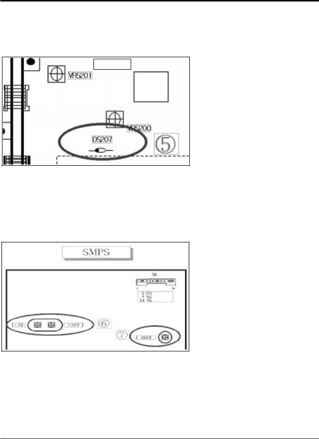
4-3 Discharge Voltage Adjustment Method (Monitor) in Times of ASS’Y Repair and Replacement
-All VR (Variable Resistor), except for VR for Vs, voltage goes down when turned counterclockwise.
● Vsc and Vy Adjustment Method
Y- Main
● Vs and Va Adjustment Method
■Vsc is the voltage of the left terminal for D5207
■Voltage adjustment is made for Vsc by using VR5201
■Standard voltage for Vsc is –55V±10V
■Vy is the voltage of the right terminal for D5207
■Voltage adjustment is made for Vy by using VR5200
■Standard voltage for Vy is 132V±10V
■Vs is the voltage of the no.11 PIN of SX Connector.
■Voltage adjustment is made for Vs by using VR in 7
■Vs is 175±5V
■Va is the voltage of the no.7 PIN of SX Connector.
■Voltage adjustment is made for Va by using right VR in 6
■Va is 75±5V
Samsung Electronics |
4-11 |

Alignment and Adjustments
■ Vw is the voltage of the right terminal
for R4414
■ Voltage adjustment is made for Vw by
using VR4400
■ Standard voltage for Vw is 175V±5V
4-12 |
Samsung Electronics |
Alignment and Adjustments
4-4 Fault Finding Using MULTI METER
Parts defects can be found for DIODE TRANSISTOR IC, using MULTI TEST including
Forward/Reverse direction Multi Test. Of course, in case resistance of several ohms and COIL are connected in parallel circuit, the lock out circuit parallel connected to part must be severed.
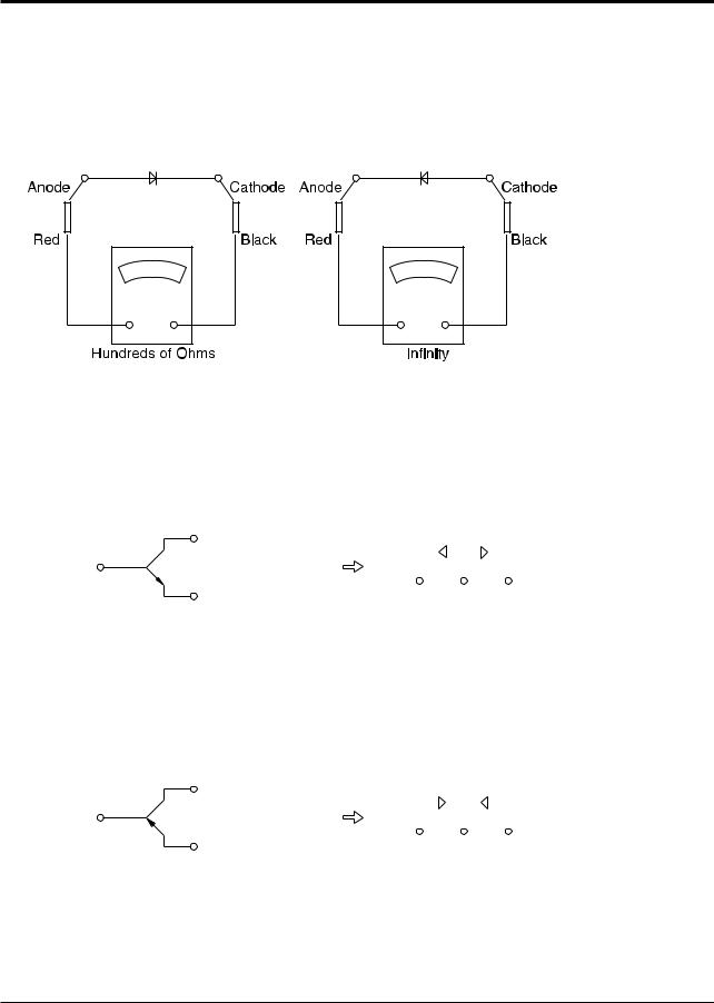
1.DIODE
+ |
- |
+ |
- |
|
Forward Direction |
Reverse Direction |
|
|
|
Between Anode and Cathode |
Hundreds of ohms |
Infinity |
|
|
|
2.TRANSISTOR
●For NPN(KSC815-Y, 2SC2068, 2SC2331-Y)
|
|
|
C (COLLECTOR) |
|
|
|
|
|
|
|
|
|
|
|
B(BASE) |
|
|
|
|
|
|
|
|
|
|
|
|
|
|
|
|
|
|
|
|
|
|
|
|
|
|
|
||
|
|
|
|
|
|
|
|
|
|
|
|
|
|
|
|
|
|
E (EMITTER) |
E |
|
|
B |
C |
||||||
|
|
|
|
|
|
|
|
|
|
|
|
|
||
|
|
|
|
|
|
|
|
|||||||
|
|
|
|
Forward Direction |
|
|
Reverse Direction |
|||||||
Between B and E |
|
Hundreds of ohms |
|
|
|
|
Infinity |
|
|
|||||
Between B and C |
|
Hundreds of ohms |
|
|
|
|
Infinity |
|
|
|||||
Between E and C |
|
Infinity |
|
|
|
|
Infinity |
|
|
|||||
● For PNP(KSA539-Y) |
|
|
|
|
|
|
|
|
|
|
|
|
||
|
|
|
C (COLLECTOR) |
|
|
|
|
|
|
|
|
|
|
|
B(BASE) |
|
|
|
|
|
|
|
|
|
|
|
|
|
|
|
|
|
|
|
|
|
|
|
|
|
|
|
|
|
|
|
|
E (EMITTER) |
E |
|
|
B |
C |
||||||
|
|
|
|
|
|
|
|
|
|
|
|
|
||
|
|
|
|
|
|
|
|
|||||||
|
|
|
|
Forward Direction |
|
|
Reverse Direction |
|||||||
Between B and E |
|
Hundreds of ohms |
|
|
|
|
Infinity |
|
|
|||||
Between B and C |
|
Hundreds of ohms |
|
|
|
|
Infinity |
|
|
|||||
Between E and C |
|
Infinity |
|
|
|
|
Infinity |
|
|
|||||
Samsung Electronics |
4-13 |

Alignment and Adjustments
3. IC (INTEGRATED CIRCUIT)
IC has built in DIODE against overvoltage in PIN. Generally, except for internal circuit defects, IC defects can be found, by measuring the DIODE.
Forward Direction |
Hundreds of ohms |
|
Reverse Direction |
Varying depending on IC but generally normal |
|
Infinity in DIODE TEST MODE |
||
|
Defects have SHORT(0 ohm) for both forward and reverse direction.
4-14 |
Samsung Electronics |

Circuit Operation Description
5. Circuit Description
5-1 Power supply
5-1-1 Outline(PDP SMPS)
Considering various related conditions, the switching regulator with good efficiency and allowing for its small size and lightweight was used as the power supply for PDP. Most of the power supply components used forward converter, and Vsamp and Vsb used simple flyback converter.
To comply with the international harmonics standards and improve the power factor, active PFC (Power Factor Correction) was used to rectify AC input into +400V DC output, which in turns used as input to the switching regulator.
5-1-2 42"SD SMPS SPECIFICATION
5-1-2(A) INPUT
PDP-42PS board is designed so that input power can be used within AC 90 VAC to 264 VAC with 50/60Hz ± 3Hz.
5-1-2(B) OUTPUT
PDP-42PS board provides 13 output switching power supplies for PDP 50inch (+165Vs, +220Set, +185Ve, +75Va, +80Scan, +18Vg, +5Vsb, +5V(D), +5V(A), +12V. +9V, +12Vfan, and +12Vsamp). The output voltage, and current requirements for continuous operation are stated below (Table 3).
Table1. Specifications of Output Power Supplies for PDP SMPS
Output Name |
Output Voltage |
Output Current |
Using in PDP driving |
|
|
|
|
|
|
|
|
Vs |
+165V |
1.4A |
Sustain Voltage of Drive Board |
|
|
|
|
Va |
+75V |
0.5A |
Address Voltage of Drive Board |
|
|
|
|
Vscan |
+80V |
0.05A |
|
|
|
|
|
Vset |
+220V |
0.05A |
|
|
|
|
|
Ve |
+185V |
0.05A |
|
|
|
|
|
Vg |
+18.3V |
0.3A |
|
|
|
|
|
Vfan |
+12V |
0.8A |
|
|
|
|
|
V9 |
+9V |
0.3A |
|
|
|
|
|
V5(A) |
+5V |
1.0A |
Analog IC Drive Voltage of Video Board |
|
|
|
|
V5(D) |
+5.3V |
3.5A |
IC Drive Voltage of Logic Board |
|
|
|
|
Vsb |
+5V |
0.4 |
Stand-by for Remote Control |
|
|
|
|
V12 |
+12V |
1.2A |
|
|
|
|
|
Vsamp |
+12V |
1.5A |
|
|
|
|
|
Samsung Electronics |
5-1 |

Circuit Operation Description
Table 2. Specifications to Protect PDP SMPS
Division |
OCP Current |
OVP Voltage |
Short Circuit |
|
|
|
|
|
|
|
|
Vs |
5A |
195V |
O.K |
|
|
|
|
Va |
2A |
90V |
O.K |
|
|
|
|
+5V |
10A |
6.2V |
O.K |
|
|
|
|
5-1-2(C) FUNCTION OF BOARD
(1)Remote control
Using 250V/ 10A relay, the board makes remote control available.
(2)Free voltage
The board designed so that input voltage can be used within 90 VAC to 264VAC.
(3)Embedded thermal sensor
The board is equipped with thermal sensor to detect the internal temperature of the unit, and to short relay when the internal temperature is higher than specified temperature so as to shutdown the unit.
(4)Improvement of power factor
The board is designed using PFC circuit so that PF (Power Factor) can be over 0.95, because low PF can be a problem in high voltage power.
(5)Protection
The OCP (Over Current Protection), the OVP (Over voltage Protection), and the Short Circuit Protection functions are added against system malfunction.
5-2 |
Samsung Electronics |

Circuit Operation Description
5-1-2(D) PDP-PS-42 BLOCK DIAGRAM
|
|
|
|
|
|
|
|
|
|
|
|
|
|
|
|
|
|
|
|
|
|
|
|
|
|
|
|
|
|
|
|
|
|
|
|
|
|
|
|
|
|
|
|
|
|
|
|
|
|
|
|
|
|
|
|
|
|
|
|
|
|
|
|
|
|
|
|
|
|
|
|
|
|
|
|
|
|
|
|
|
|
|
|
|
|
|
|
|
|
|
|
|
|
|
|
|
|
|
|
|
|
|
|
|
|
|
|
|
|
|
|
|
|
|
|
|
|
|
|
|
|
|
|
|
|
|
|
|
|
|
|
|
|
|
|
|
|
|
|
|
|
|
|
|
|
|
|
|
|
|
|
|
|
|
|
|
|
|
|
|
|
|
|
|
|
|
|
|
|
|
|
|
|
|
|
|
|
|
|
|
|
|
|
|
|
|
|
|
|
|
|
|
|
|
|
|
|
|
|
|
|
|
|
|
|
|
|
|
|
|
|
|
|
|
|
|
|
|
|
|
|
|
|
|
|
|
|
|
|
|
|
|
|
|
|
|
|
|
|
|
|
|
|
|
|
|
|
|
|
|
|
|
|
|
|
|
|
|
|
|
|
|
|
|
|
|
|
|
|
|
|
|
|
|
|
|
|
|
|
|
|
|
|
|
|
|
|
|
|
|
|
|
|
|
|
|
|
|
|
|
|
|
|
|
|
|
|
|
|
|
|
|
|
|
|
|
|
|
|
|
|
|
|
|
|
|
|
|
|
|
|
|
|
|
|
|
|
|
|
|
|
|
|
|
|
|
|
|
|
|
|
|
|
|
|
|
|
|
|
|
|
|
|
|
|
|
|
|
|
|
|
|
|
|
|
|
|
|
|
|
|
|
|
|
|
|
|
|
|
|
|
|
|
|
|
|
|
|
|
|
|
|
|
|
|
|
|
|
|
|
|
|
|
|
|
|
|
|
|
|
|
|
|
|
|
|
|
|
|
|
|
|
|
|
|
|
|
|
|
|
|
|
|
|
|
|
|
|
|
|
|
|
|
|
|
|
|
|
|
|
|
|
|
|
|
|
|
|
|
|
|
|
|
|
|
|
|
|
|
|
|
|
|
|
|
|
|
|
|
|
|
|
|
|
|
|
|
|
|
|
|
|
|
|
|
|
|
|
|
|
|
|
|
|
|
|
|
|
|
|
|
|
|
|
|
|
|
|
|
|
|
|
|
|
|
|
|
|
|
|
|
|
|
|
|
|
|
|
|
|
|
|
|
|
|
|
|
|
|
|
|
|
|
|
|
|
|
|
|
|
|
|
|
|
|
|
|
|
|
|
|
|
|
|
|
|
|
|
|
|
|
|
|
|
|
|
|
|
|
|
|
|
|
|
|
|
|
|
|
|
|
|
|
|
|
|
|
|
|
|
|
|
|
|
|
|
|
|
|
|
|
|
|
|
|
|
|
|
|
|
|
|
|
|
|
|
|
|
|
|
|
|
|
|
|
|
|
|
|
|
|
|
|
|
|
|
|
|
|
|
|
|
|
|
|
|
|
|
|
|
|
|
|
|
|
|
|
|
|
|
|
|
|
|
|
|
|
|
|
|
|
|
|
|
|
|
|
|
|
|
|
|
|
|
|
|
|
|
|
|
|
|
|
|
|
|
|
|
|
|
|
|
|
|
|
|
|
|
|
|
|
|
|
|
|
|
|
|
|
|
|
|
|
|
|
|
|
|
|
|
|
|
|
|
|
|
|
|
|
|
|
|
|
|
|
|
|
|
|
|
|
|
|
|
|
|
|
|
|
|
|
|
|
|
|
|
|
|
|
|
|
|
|
|
|
|
|
|
|
|
|
|
|
|
|
|
|
|
|
|
|
|
|
|
|
|
|
|
|
|
|
|
|
|
|
|
|
|
|
|
|
|
|
|
|
|
|
|
|
|
|
|
|
|
|
|
|
|
|
|
|
|
|
|
|
|
|
|
|
|
|
|
|
|
|
|
|
|
|
|
|
|
|
|
|
|
|
|
|
|
|
|
|
|
|
|
|
|
|
|
|
|
|
|
|
|
|
|
|
|
|
|
|
|
|
|
|
|
|
|
|
|
|
|
|
|
|
|
|
|
|
|
|
|
|
|
|
|
|
|
|
|
|
|
|
|
|
|
|
|
|
|
|
|
|
|
|
|
|
|
|
|
|
|
|
|
|
|
|
|
|
|
|
|
|
|
|
|
|
|
|
|
|
|
|
|
|
|
|
|
|
|
|
|
|
|
|
|
|
|
|
|
|
|
|
|
|
|
|
|
|
|
|
|
|
|
|
|
|
|
|
|
|
|
|
|
|
|
|
|
|
|
|
|
|
|
|
|
|
|
|
|
|
|
|
|
|
|
|
|
|
|
|
|
|
|
|
|
|
|
|
|
|
|
|
|
|
|
|
|
|
|
|
|
|
|
|
|
|
|
|
|
|
|
|
|
|
|
|
|
|
|
|
|
|
|
|
|
|
|
|
|
|
|
|
|
|
|
|
|
|
|
|
|
|
|
|
|
|
|
|
|
|
|
|
|
|
|
|
|
|
|
|
|
|
|
|
|
|
|
|
|
|
|
|
|
|
|
|
|
|
|
|
|
|
|
|
|
|
|
|
|
|
|
|
|
|
|
|
|
|
|
|
|
|
|
|
|
|
|
|
|
|
|
|
|
|
|
|
|
|
|
|
|
|
|
|
|
|
|
|
|
|
|
|
|
|
|
|
|
|
|
|
|
|
|
|
|
|
|
|
|
|
|
|
|
|
|
|
|
|
|
|
|
|
|
|
|
|
|
|
|
|
|
|
|
|
|
|
|
|
|
|
|
|
|
|
|
|
|
|
|
|
|
|
|
|
|
|
|
|
|
|
|
|
|
|
|
|
|
|
|
|
|
|
|
|
|
|
|
|
|
|
|
|
|
|
|
|
|
|
|
|
|
|
|
|
|
|
|
|
|
|
|
|
|
|
|
|
|
|
|
|
|
|
|
|
|
|
|
|
|
|
|
|
|
|
|
|
|
|
|
|
|
|
|
|
|
|
|
|
|
|
|
|
|
|
|
|
|
|
|
|
|
|
|
|
|
|
|
|
|
|
|
|
|
|
|
|
|
|
|
|
|
|
|
|
|
|
|
|
|
|
|
|
|
|
|
|
|
|
|
|
|
|
|
|
|
|
|
|
|
|
|
|
|
|
|
|
|
|
|
|
|
|
|
|
|
|
|
|
|
|
|
|
|
|
|
|
|
|
|
|
|
|
|
|
|
|
|
|
|
|
|
|
|
|
|
|
|
|
|
|
|
|
|
|
|
|
|
|
|
|
|
|
|
|
|
|
|
|
|
|
|
|
|
|
|
|
|
|
|
|
|
|
|
|
|
|
|
|
|
|
|
|
|
|
|
|
|
|
|
|
|
|
|
|
|
|
|
|
|
|
|
|
|
|
|
|
|
|
|
|
|
|
|
|
|
|
|
|
|
|
|
|
|
|
|
|
|
|
|
|
|
|
|
|
|
|
|
|
|
|
|
|
|
|
|
|
|
|
|
|
|
|
|
|
|
|
|
|
|
|
|
|
|
|
|
|
|
|
|
|
|
|
|
|
|
|
|
|
|
|
|
|
|
|
|
|
|
|
|
|
|
|
|
|
|
|
|
|
|
|
|
|
|
|
|
|
|
|
|
|
|
|
|
|
|
|
|
|
|
|
|
|
|
|
|
|
|
|
|
|
|
|
|
|
|
|
|
|
|
|
|
|
|
|
|
|
|
|
|
|
|
|
|
|
|
|
|
|
|
|
|
|
|
|
|
|
|
|
|
|
|
|
|
|
|
|
|
|
|
|
|
|
|
|
|
|
|
|
|
|
|
|
|
|
|
|
|
|
|
|
|
|
|
|
|
|
|
|
|
|
|
|
|
|
|
|
|
|
|
|
|
|
|
|
|
|
|
|
|
|
|
|
|
|
|
|
|
|
|
|
|
|
|
|
|
|
|
|
|
|
|
|
|
|
|
|
|
|
|
|
|
|
|
|
|
|
|
|
|
|
|
|
|
|
|
|
|
|
|
|
|
|
|
|
|
|
|
|
|
|
|
|
|
|
|
|
|
|
|
|
|
|
|
|
|
|
|
|
|
|
|
|
|
|
|
|
|
|
|
|
|
|
|
|
|
|
|
|
|
|
|
|
|
|
|
|
|
|
|
|
|
|
|
|
|
|
|
|
|
|
|
|
|
|
|
|
|
|
|
|
|
|
|
|
|
|
|
|
|
|
|
|
|
|
|
|
|
|
|
|
|
|
|
|
|
|
|
|
|
|
|
|
|
|
|
|
|
|
|
|
|
|
|
|
|
|
|
|
|
|
|
|
|
|
|
|
|
|
|
|
|
|
|
|
|
|
|
|
|
|
|
|
|
|
|
|
|
|
|
|
|
|
|
|
|
|
|
|
|
|
|
|
|
|
|
|
|
|
|
|
|
|
|
|
|
|
|
|
|
|
|
|
|
|
|
|
|
|
|
|
|
|
|
|
|
|
|
|
|
|
|
|
|
|
|
|
|
|
|
|
|
|
|
|
|
|
|
|
|
|
|
|
|
|
|
|
|
|
|
|
|
|
|
|
|
|
|
|
|
|
|
|
|
|
|
|
|
|
|
|
|
|
|
|
|
|
|
|
|
|
|
|
|
|
|
|
|
|
|
|
|
|
|
|
|
|
|
|
|
|
|
|
|
|
|
|
|
|
|
|
|
|
|
|
|
|
|
|
|
|
|
|
|
|
|
|
|
|
|
|
|
|
|
|
|
|
|
|
|
|
|
|
|
|
|
|
|
|
|
|
|
|
|
|
|
|
|
|
|
|
|
|
|
|
|
|
|
|
|
|
|
|
|
|
|
|
|
|
|
|
|
|
|
|
|
|
|
|
|
|
|
|
|
|
|
|
|
|
|
|
|
|
|
|
|
|
|
|
|
|
|
|
|
|
|
|
|
|
|
|
|
|
|
|
|
|
|
|
|
|
|
|
|
|
|
|
|
|
|
|
|
|
|
|
|
|
|
|
|
|
|
|
|
|
|
|
|
|
|
|
|
|
|
|
|
|
|
|
|
|
|
|
|
|
|
|
|
|
|
|
|
|
|
|
|
|
|
|
|
|
|
|
|
|
|
|
|
|
|
|
|
|
|
|
|
|
|
|
|
|
|
|
|
|
|
|
|
|
|
|
|
|
|
|
|
|
|
|
|
|
|
|
|
|
|
|
|
|
|
|
|
|
|
|
|
|
|
|
|
|
|
|
|
|
|
|
|
|
|
|
|
|
|
|
|
|
|
|
|
|
|
|
|
|
|
|
|
|
|
|
|
|
|
|
|
|
|
|
|
|
|
|
|
|
|
|
|
|
|
|
|
|
|
|
|
|
|
|
|
|
|
|
|
|
|
|
|
|
|
|
|
|
|
|
|
|
|
|
|
|
|
|
|
|
|
|
|
|
|
|
|
|
|
|
|
|
|
|
|
|
|
|
|
|
|
|
|
|
|
|
|
|
|
|
|
|
|
|
|
|
|
|
|
|
|
|
|
|
|
|
|
|
|
|
|
|
|
|
|
|
|
|
|
|
|
|
|
|
|
|
|
|
|
|
|
|
|
|
|
|
|
|
|
|
|
|
|
|
|
|
|
|
|
|
|
|
|
|
|
|
|
|
|
|
|
|
|
|
|
|
|
|
|
|
|
|
|
|
|
|
|
|
|
|
|
|
|
|
|
|
|
|
|
|
|
|
|
|
|
|
|
|
|
|
|
|
|
|
|
|
|
|
|
|
|
|
|
|
|
|
|
|
|
|
|
|
|
|
|
|
|
|
|
|
|
|
|
|
|
|
|
|
|
|
|
|
|
|
|
|
|
|
|
|
|
|
|
|
|
|
|
|
|
|
|
|
|
|
|
|
|
|
|
|
|
|
|
|
|
|
|
|
|
|
|
|
|
|
|
|
|
|
|
|
|
|
|
|
|
|
|
|
|
|
|
|
|
|
|
|
|
|
|
|
|
|
|
|
|
|
|
|
|
|
|
|
|
|
|
|
|
|
|
|
|
|
|
|
|
|
|
|
|
|
|
|
|
|
|
|
|
|
|
|
|
|
|
|
|
|
|
|
|
|
|
|
|
|
|
|
|
|
|
|
|
|
|
|
|
|
|
|
|
|
|
|
|
|
|
|
|
|
|
|
|
|
|
|
|
|
|
|
|
|
|
|
|
|
|
|
|
|
|
|
|
|
|
|
|
|
|
|
|
|
|
|
|
|
|
|
|
|
|
|
|
|
|
|
|
|
|
|
|
|
|
|
|
|
|
|
|
|
|
|
|
|
|
|
|
|
|
|
|
|
|
|
|
|
|
|
|
|
|
|
|
|
|
|
|
|
|
|
|
|
|
|
|
|
|
|
|
|
|
|
|
|
|
|
|
|
|
|
|
|
|
|
|
|
|
|
|
|
|
|
|
|
|
|
|
|
|
|
|
|
|
|
|
|
|
|
|
|
|
|
|
|
|
|
|
|
|
|
|
|
|
|
|
|
|
|
|
|
|
|
|
|
|
|
|
|
|
|
|
|
|
|
|
|
|
|
|
|
|
|
|
|
|
|
|
|
|
|
|
|
|
|
|
|
|
|
|
|
|
|
|
|
|
|
|
|
|
|
|
|
|
|
|
|
|
|
|
|
|
|
|
|
|
|
|
|
|
|
|
|
|
|
|
|
|
|
|
|
|
|
|
|
|
|
|
|
|
|
|
|
|
|
|
|
|
|
|
|
|
|
|
|
|
|
|
|
|
|
|
|
|
|
|
|
|
|
|
|
|
|
|
|
|
|
|
|
|
|
|
|
|
|
|
|
|
|
|
|
|
|
|
|
|
|
|
|
|
|
|
|
|
|
|
|
|
|
|
|
|
|
|
|
|
|
|
|
|
|
|
|
|
|
|
|
|
|
|
|
|
|
|
|
|
|
|
|
|
|
|
|
|
|
|
|
|
|
|
|
|
|
|
|
|
|
|
|
|
|
|
|
|
|
|
|
|
|
|
|
|
|
|
|
|
|
|
|
|
|
|
|
|
|
|
|
|
|
|
|
|
|
|
|
|
|
|
|
|
|
|
|
|
|
|
|
|
|
|
|
|
|
|
|
|
|
|
|
|
|
|
|
|
|
|
|
|
|
|
|
|
|
|
|
|
|
|
|
|
|
|
|
|
|
|
|
|
|
|
|
|
|
|
|
|
|
|
|
|
|
|
|
|
|
|
|
|
|
|
|
|
|
|
|
|
|
|
|
|
|
|
|
|
|
|
|
|
|
|
|
|
|
|
|
|
|
|
|
|
|
|
|
|
|
|
|
|
|
|
|
|
|
|
|
|
|
|
|
|
|
|
|
|
|
|
|
|
|
|
|
|
|
|
|
|
|
|
|
|
|
|
|
|
|
|
|
|
|
|
|
|
|
|
|
|
|
|
|
|
|
|
|
|
|
|
|
|
|
|
|
|
|
|
|
|
|
|
|
|
|
|
|
|
|
|
|
|
|
|
|
|
|
|
|
|
|
|
|
|
|
|
|
|
|
|
|
|
|
|
|
|
|
|
|
|
|
|
|
|
|
|
|
|
|
|
|
|
|
|
|
|
|
|
|
|
|
|
|
|
|
|
|
|
|
|
|
|
|
|
|
|
|
|
|
|
|
|
|
|
|
|
|
|
|
|
|
|
|
|
|
|
|
|
|
|
|
|
|
|
|
|
|
|
|
|
|
|
|
|
|
|
|
|
|
|
|
|
|
|
|
|
|
|
|
|
|
|
|
|
|
|
|
|
|
|
|
|
|
|
|
|
|
|
|
|
|
|
|
|
|
|
|
|
|
|
|
|
|
|
|
|
|
|
|
|
|
|
|
|
|
|
|
|
|
|
|
|
|
|
|
|
|
|
|
|
|
|
|
|
|
|
|
|
|
|
|
|
|
|
|
|
|
|
|
|
|
|
|
|
|
|
|
|
|
|
|
|
|
|
|
|
|
|
|
|
|
|
|
|
|
|
|
|
|
|
|
|
|
|
|
|
|
|
|
|
|
|
|
|
|
|
|
|
|
|
|
|
|
|
|
|
|
|
|
|
|
|
|
|
|
|
|
|
|
|
|
|
|
|
|
|
|
|
|
|
|
|
|
|
|
|
|
|
|
|
|
|
|
|
|
|
|
|
|
|
|
|
|
|
|
|
|
|
|
|
|
|
|
|
|
|
|
|
|
|
|
|
|
|
|
|
|
|
|
|
|
|
|
|
|
|
|
|
|
|
|
|
|
|
|
|
|
|
|
|
|
|
|
|
|
|
|
|
|
|
|
|
|
|
|
|
|
|
|
|
|
|
|
|
|
|
|
|
|
|
|
|
|
|
|
|
|
|
|
|
|
|
|
|
|
|
|
|
|
|
|
|
|
|
|
|
|
|
|
|
|
|
|
|
|
|
|
|
|
|
|
|
|
|
|
|
|
|
|
|
|
|
|
|
|
|
|
|
|
|
|
|
|
|
|
|
|
|
|
|
|
|
|
|
|
|
|
|
|
|
|
|
|
|
|
|
|
|
|
|
|
|
|
|
|
|
|
|
|
|
|
|
|
|
|
|
|
|
|
|
|
|
|
|
|
|
|
|
|
|
|
|
|
|
|
|
|
|
|
|
|
|
|
|
|
|
|
|
|
|
|
|
|
|
|
|
|
|
|
|
|
|
|
|
|
|
|
|
|
|
|
|
|
|
|
|
|
|
|
|
|
|
|
|
|
|
|
|
|
|
|
|
|
|
|
|
|
|
|
|
|
|
|
|
|
|
|
|
|
|
|
|
|
|
|
|
|
|
|
|
|
|
|
|
|
|
|
|
|
|
|
|
|
|
|
|
|
|
|
|
|
|
|
|
|
|
|
|
|
|
|
|
|
|
|
|
|
|
|
|
|
|
|
|
|
|
|
|
|
|
|
|
|
|
|
|
|
|
|
|
|
|
|
|
|
|
|
|
|
|
|
|
|
|
|
|
|
|
|
|
|
|
|
|
|
|
|
|
|
|
|
|
|
|
|
|
|
|
|
|
|
|
|
|
|
|
|
|
|
|
|
|
|
|
|
|
|
|
|
|
|
|
|
|
|
|
|
|
|
|
|
|
|
|
|
|
|
|
|
|
|
|
|
|
|
|
|
|
|
|
|
|
|
|
|
|
|
|
|
|
|
|
|
|
|
|
|
|
|
|
|
|
|
|
|
|
|
|
|
|
|
|
|
|
|
|
|
|
|
|
|
|
|
|
|
|
|
|
|
|
|
|
|
|
|
|
|
|
|
|
|
|
|
|
|
|
|
|
|
|
|
|
|
|
|
|
|
|
|
|
|
|
|
|
|
|
|
|
|
|
|
|
|
|
|
|
|
|
|
|
|
|
|
|
|
|
|
|
|
|
|
|
|
|
|
|
|
|
|
|
|
|
|
|
|
|
|
|
|
|
|
|
|
|
|
|
|
|
|
|
|
|
|
|
|
|
|
|
|
|
|
|
|
|
|
|
|
|
|
|
|
|
|
|
|
|
|
|
|
|
|
|
|
|
|
|
|
|
|
|
|
|
|
|
|
|
|
|
|
|
|
|
|
|
|
|
|
|
|
|
|
|
|
|
|
|
|
|
|
|
|
|
|
|
|
|
|
|
|
|
|
|
|
|
|
|
|
|
|
|
|
|
|
|
|
|
|
|
|
|
|
|
|
|
|
|
|
|
|
|
|
|
|
|
|
|
|
|
|
|
|
|
|
|
|
|
|
|
|
|
|
|
|
|
|
|
|
|
|
|
|
|
|
|
|
|
|
|
|
|
|
|
|
|
|
|
|
|
|
|
|
|
|
|
|
|
|
|
|
|
|
|
|
|
|
|
|
|
|
|
|
|
|
|
|
|
|
|
|
|
|
|
|
|
|
|
|
|
|
|
|
|
|
|
|
|
|
|
|
|
|
|
|
|
|
|
|
|
|
|
|
|
|
|
|
|
|
|
|
|
|
|
|
|
|
|
|
|
|
|
|
|
|
|
|
|
|
|
|
|
|
|
|
|
|
|
|
|
|
|
|
|
|
|
|
|
|
|
|
|
|
|
|
|
|
|
|
|
|
|
|
|
|
|
|
|
|
|
|
|
|
|
|
|
|
|
|
|
|
|
|
|
|
|
|
|
|
|
|
|
|
|
|
|
|
|
|
|
|
|
|
|
|
|
|
|
|
|
|
|
|
|
|
|
|
|
|
|
|
|
|
|
|
|
|
|
|
|
|
|
|
|
|
|
|
|
|
|
|
|
|
|
|
|
|
|
|
|
|
|
|
|
|
|
|
|
|
|
|
|
|
|
|
|
|
|
|
|
|
|
|
|
|
|
|
|
|
|
|
|
|
|
|
|
|
|
|
|
|
|
|
|
|
|
|
|
|
|
|
|
|
|
|
|
|
|
|
|
|
|
|
|
|
|
|
|
|
|
|
|
|
|
|
|
|
|
|
|
|
|
|
|
|
|
|
|
|
|
|
|
|
|
|
|
|
|
|
|
|
|
|
|
|
|
|
|
|
|
|
|
|
|
|
|
|
|
|
|
|
|
|
|
|
|
|
|
|
|
|
|
|
|
|
|
|
|
|
|
|
|
|
|
|
|
|
|
|
|
|
|
|
|
|
|
|
|
|
|
|
|
|
|
|
|
|
|
|
|
|
|
|
|
|
|
|
|
|
|
|
|
|
|
|
|
|
|
|
|
|
|
|
|
|
|
|
|
|
|
|
|
|
|
|
|
|
|
|
|
|
|
|
|
|
|
|
|
|
|
|
|
|
|
|
|
|
|
|
|
|
|
|
|
|
|
|
|
|
|
|
|
|
|
|
|
|
|
|
|
|
|
|
|
|
|
|
|
|
|
|
|
|
|
|
|
|
|
|
|
|
|
|
|
|
|
|
|
|
|
|
|
|
|
|
|
|
|
|
|
|
|
|
|
|
|
|
|
|
|
|
|
|
|
|
|
|
|
|
|
|
|
|
|
|
|
|
|
|
|
|
|
|
|
|
|
|
|
|
|
|
|
|
|
|
|
|
|
|
|
|
|
|
|
|
|
|
|
|
|
|
|
|
|
|
|
|
|
|
|
|
|
|
|
|
|
|
|
|
|
|
|
|
|
|
|
|
|
|
|
|
|
|
|
|
|
|
|
|
|
|
|
|
|
|
|
|
|
|
|
|
|
|
|
|
|
|
|
|
|
|
|
|
|
|
|
|
|
|
|
|
|
|
|
|
|
|
|
|
|
|
|
|
|
|
|
|
|
|
|
|
|
|
|
|
|
|
|
|
|
|
|
|
|
|
|
|
|
|
|
|
|
|
|
|
|
|
|
|
|
|
|
|
|
|
|
|
|
|
|
|
|
|
|
|
|
|
|
|
|
|
|
|
|
|
|
|
|
|
|
|
|
|
|
|
|
|
|
|
|
|
|
|
|
|
|
|
|
|
|
|
|
|
|
|
|
|
|
|
|
|
|
|
|
|
|
|
|
|
|
|
|
|
|
|
|
|
|
|
|
|
|
|
|
|
|
|
|
|
|
|
|
|
|
|
|
|
|
|
|
|
|
|
|
|
|
|
|
|
|
|
|
|
|
|
|
|
|
|
|
|
|
|
|
|
|
|
|
|
|
|
|
|
|
|
|
|
|
|
|
|
|
|
|
|
|
|
|
|
|
|
|
|
|
|
|
|
|
|
|
|
|
|
|
|
|
|
|
|
|
|
|
|
|
|
|
|
|
|
|
|
|
|
|
|
|
|
|
|
|
|
|
|
|
|
|
|
|
|
|
|
|
|
|
|
|
|
|
|
|
|
|
|
|
|
|
|
|
|
|
|
|
|
|
|
|
|
|
|
|
|
|
|
|
|
|
|
|
|
|
|
|
|
|
|
|
|
|
|
|
|
|
|
|
|
|
|
|
|
|
|
|
|
|
|
|
|
|
|
|
|
|
|
|
|
|
|
|
|
|
|
|
|
|
|
|
|
|
|
|
|
|
|
|
|
|
|
|
|
|
|
|
|
|
|
|
|
|
|
|
|
|
|
|
|
|
|
|
|
|
|
|
|
|
|
|
|
|
|
|
|
|
|
|
|
|
|
|
|
|
|
|
|
|
|
|
|
|
|
|
|
|
|
|
|
|
|
|
|
|
|
|
|
|
|
|
|
|
|
|
|
|
|
|
|
|
|
|
|
|
|
|
|
|
|
|
|
|
|
|
|
|
|
|
|
|
|
|
|
|
|
|
|
|
|
|
|
|
|
|
|
|
|
|
|
|
|
|
|
|
|
|
|
|
|
|
|
|
|
|
|
|
|
|
|
|
|
|
|
|
|
|
|
|
|
|
|
|
|
|
|
|
|
|
|
|
|
|
|
|
|
|
|
|
|
|
|
|
|
|
|
|
|
|
|
|
|
|
|
|
|
|
|
|
|
|
|
|
|
|
|
|
|
|
|
|
|
|
|
|
|
|
|
|
|
|
|
|
|
|
|
|
|
|
|
|
|
|
|
|
|
|
|
|
|
|
|
|
|
|
|
|
|
|
|
|
|
|
|
|
|
|
|
|
|
|
|
|
|
|
|
|
|
|
|
|
|
|
|
|
|
|
|
|
|
|
|
|
|
|
|
|
|
|
|
|
|
|
|
|
|
|
|
|
|
|
|
|
|
|
|
|
|
|
|
|
|
|
|
|
|
|
|
|
|
|
|
|
|
|
|
|
|
|
|
|
|
|
|
|
|
|
|
|
|
|
|
|
|
|
|
|
|
|
|
|
|
|
|
|
|
|
|
|
|
|
|
|
|
|
|
|
|
|
|
|
|
|
|
|
|
|
|
|
|
|
|
|
|
|
|
|
|
|
|
|
|
|
|
|
|
|
|
|
|
|
|
|
|
|
|
|
|
|
|
|
|
|
|
|
|
|
|
Samsung Electronics |
5-3 |
||||||||||||||||||||||||||||||||||||||||||||||||||||||||||||||||||||||||||||

Circuit Operation Description
(1)AC-DC Converter
PDP-42PS outputs +400V DC from the common AC power supply using the active PFC booster converter. This converter is designed for improving the power factor and preventing the noise with high frequency and finally becomes the input power system for the switching regulator on the output side.
(2)Auxiliary Power Supply
The auxiliary power supply is a block generating power of •Ï-com for remote controlling. Once the power plug is inserted, this block always comes into operation, causing •Ï-com to get into the standby state for the output. Thus, this output is called the stand-by voltage. And with the relay ON signal inputted through the remote controller, this block turns the mechanical switch of relay to ON for driving the main power supply.
(3)Implementation of Sustain Voltage
As the main part of a SMPS for PDP, sustain voltage must supply a high power, +165V/ 1.4A. It is designed using forward converter basically. At the output stage two 90V converters are connected serially for high efficiency and reduction of system size against a single 180V converter.
(4)Implementation of Small Power Output (Va, V(D), V(A), Vfan, V9, Vsamp, Ve, Vset, Vscan, V12, and Vg)Vset, Ve, and Vscan used DC-DC module. V(D), Va, V12, and Vfan used forward converter, and Vsamp used flyback converter. V(A), V9, and Vg are simply implemented using switching regulator.
5-1-3 Requirements of PDP SMPS
Since SMPS does not operate alone, but it operates with the load of the whole system, it should be designed carefully considering the load of the system. In addition, it should be designed considering emerging issues such as EMC, and protection against heat as well as system stability especially.
5-1-3(A) SAFETY AND REMOTE CONTROL CAPABILITY
Stability is one of the most important requirements for SMPS. SMPS should be designed to prevent abnormal status due to abnormal load variation so as to keep the system stable, and guarantee customer safety.
The protection circuits of SMPS include over-current protection (OCP), over voltage protection (OVP), and under voltage lock-out (UVLO), and short circuit protection circuit. Although each circuit can be implemented by various procedures, the most popular is implementing with comparator that compares current value with that of standard and determine abnormality of the circuit.
In addition, surge current protection, insulation management, and static electricity protection circuit should be added, because it uses commercial power source as an input.
PDP SMPS should be designed using auxiliary power and relay to provide remote control capability.
5-4 |
Samsung Electronics |
Circuit Operation Description
5-1-3(B) THE RELATION BETWEEN POWER CONSUMPTION AND POWER CONVERSION Efficiency
The power consumption and the power conversion efficiency of SMPS affect protection against heat and system operation much.
[ If the power conversion efficiency of 100W SMPS is 70%, is the power loss of internal circuit 30W? ] Output power consumption Po is determined by the multiplication of DC output voltage Vo and output current Io. Input power consumption Pi is determined by the addition of output power consumption Po and internal power loss of SMPS Pl.
Provided that the power conversion efficiency is _,
If the power conversion efficiency of 100W SMPS is 70%, the internal power loss is about 42.8W by Equation (1). If the power conversion efficiency of 400W SMPS for 42"SD is 82%, the internal power loss is 87.8W by Equation (1). Table 4 shows internal power loss as a function of output power for various power conversion efficiencies.
|
200 |
|
|
|
|
|
|
η=50% |
|
|
|
|
|
|
|
|
|
|
|
|
|
180 |
|
|
|
|
|
|
|
|
|
|
|
|
|
|
|
|
|
|
|
|
|
|
|
|
|
|
|
|
|
|
|
|
|
|
|
|
|
|
|
|
|
|
|
|
|
|
|
|
|
|
|
|
|
η=60% |
|
|
|
|
|
||
|
160 |
|
|
|
|
|
|
|
|
|
|
|
|
|
|
|
|
|
||
|
|
|
|
|
|
|
|
|
|
|
|
|
|
|
|
|
|
|
|
|
|
|
|
|
|
|
|
|
|
|
|
|
|
|
|
|
|
|
|
|
|
|
140 |
|
|
|
|
|
|
|
|
|
|
|
|
|
|
|
|
|
|
|
|
|
|
|
|
|
|
|
|
|
|
|
|
|
|
η=70% |
|
|
|
||
|
120 |
|
|
|
|
|
|
|
|
|
|
|
|
|
|
|
|
|
||
Internal |
|
|
|
|
|
|
|
|
|
|
|
|
|
|
|
|
|
|
|
|
|
|
|
|
|
|
|
|
|
|
|
|
|
|
|
|
|
|
|
||
|
|
|
|
|
|
|
|
|
|
|
|
|
|
|
|
|
|
|
|
|
Power |
100 |
|
|
|
|
|
|
|
|
|
|
|
|
|
|
|
|
|
|
|
|
|
|
|
|
|
|
|
|
|
|
|
|
|
|
|
|
|
|
||
Loss ( W) |
|
|
|
|
|
|
|
|
|
|
|
|
|
|
|
|
|
|
|
|
80 |
|
|
|
|
|
|
|
|
|
|
|
|
|
|
|
|
|
|
|
|
|
|
|
|
|
|
|
|
|
|
|
|
|
|
|
|
|
|
|
|
|
|
|
|
|
|
|
|
|
|
|
|
|
|
|
|
η= 80% |
|
|
|
||
|
60 |
|
|
|
|
|
|
|
|
|
|
|
|
|
|
|
|
|
||
|
|
|
|
|
|
|
|
|
|
|
|
|
|
|
|
|
|
|
|
|
|
|
|
|
|
|
|
|
|
|
|
|
|
|
|
|
|
|
|
|
|
|
40 |
|
|
|
|
|
|
|
|
|
|
|
|
|
|
|
|
|
|
|
|
|
|
|
|
|
|
|
|
|
|
|
|
|
|
η=90% |
|
|
|
||
|
|
|
|
|
|
|
|
|
|
|
|
|
|
|
|
|
|
|
||
|
20 |
|
|
|
|
|
|
|
|
|
|
|
|
|
|
|
|
|
|
|
|
|
|
|
|
|
|
|
|
|
|
|
|
|
|
|
|
|
|
|
|
|
0 |
|
|
|
|
|
|
|
|
|
|
|
|
|
|
|
|
|
|
|
|
|
|
|
|
|
|
|
|
|
|
|
|
|
|
|
|
|
|
|
|
|
120 |
140 |
160 |
180 |
200 |
220 |
240 |
260 |
280 |
300 |
||||||||||
Direct Current Output Power (W)
Table 4. Power Conversion Efficiency vs. Internal Power Loss
Samsung Electronics |
5-5 |

Circuit Operation Description
5-1-3(C) PFC (Power Factor Correction) Circuit Descriptions
The current electric devices use DC power supply and require a rectifier circuit converting AC into DC. As most rectifier circuits apply a capacitor input type, the rectifier circuit becomes the core of the occurrence of harmonics with lower reverse rate.If various electronic and electric devices are connected to a power system, high-frequency current will occur due to a power rectifier circuit, a phase control circuit with power input current of non-sine wave, or components with non-linear load characteristics, such as capacitor, inductor, etc. As the result, the disturbance of voltage occurs, and finally a power capacitor or a transformer generates heat, fire or noise occurs, controls malfunction, or the accessed devices abnormally operate or their lives are shortened.To prevent those symptoms, IEC (International Electrotechnical Commission) regulated standards for Power Supply Harmonics.
(Refer to IEC 1000-3-2.)Figure 8 shows the basic structure of Active Boost PFC and waveforms.
Standards for Power Supply Harmonics
Scale: Devices accessed to 220V/380V, 230V/400V, 240V/425V and lower than 16A (IEC 100-3-2) Devices with AC 230V and lower than 16A (IEC 555-2)
Applied Classes :
♣Class A : Devices not included in another class
♣Class B : Portable tools
♣Class C : Lighting devices
♣Class D : Devices with special current waveforms
Application Schedule : Except the devices less than rating input of 75W (1996~1999) Except the devices less than rating input of 50W (2000 and after)
5-6 |
Samsung Electronics |

Circuit Operation Description
The architecture and the pulse of active boost PFC
5-1-3(D) CONCLUSION
Although SMPS (Switching Mode Power Supply) enables small lightweight high-power consumption power design, it is hard to be used when stability and precise control are required. Power stage for PDP can be designed using the lightweight SMPS feature. It is important to design SMPS considering system load, stability, and related international standards.
Samsung Electronics |
5-7 |

Circuit Operation Description
5-2 Driver Circuit
5-2-1 Driver Circuit Overview
5-2-1(A) WHAT IS THE DEFINITION OF DRIVE CIRCUIT?
It is a circuit generating an appropriate pulse (High voltage pulse) and then driving the panel to implement images in the external terminals (X electrode group, Y electrode group and address electrode), and this high voltage switching pulse is generated by a combination of MOSFET’s.
5-2-1(B) PANEL DRIVING PRINCIPLES
In PDP, images are implemented by impressing voltage on the X electrode, Y electrode and address electrode, components of each pixel on the panel, under appropriate conditions. Currently, ADS (Address & Display Separate: Driving is made by separating address and sustaining sections) is most widely used to generate the drive pulse. Discharges conducted within PDP pixels using this method can largely be classified into 3 types, as follows:
(1)Address discharge : This functions to generate wall voltage within pixels to be lighted by addressing information to them (i.e., impressing data voltage)
(2)Sustain discharge : This means a display section where only pixels with wall voltage by the address discharge display self-sustaining discharge by the support of such wall voltage. (Optic outputs realizing images are generated.)
(3)Erase discharge : To have address discharge occur selectively in pixels, all pixels in the panel must have the same conditions (i.e., the same state of wall and space electric discharges). The ramp reset discharge section, therefore, is important to secure the drive margin, and methods most widely used to date include wall voltage controlling by ramp pulse.
5-8 |
Samsung Electronics |

Circuit Operation Description
5-2-1(C) TYPES AND DETAILED EXPLANATION OF DRIVE DISCHARGES
(1 ) Sustaining discharge
Sustaining discharge means a self-sustaining discharge generated by the total of the sustaining pulse voltage (usually, 160~170V) alternately given to X and Y electrodes during the sustaining period and the wall voltage that varies depending upon pixels' previous discharge status. It is operated by the memory function (through this, the current status is defined by previous operation conditions) AC PDP basically possesses. That is, when there is existing wall voltage in pixels (in other words, when pixels remain ON), the total of wall voltage and a sustaining voltage to be impressed subsequently impresses a voltage equal to or above the discharge start voltage, thereby generating discharge again, but when there is no existing wall voltage in pixels (in other words, when pixels remain OFF), the sustaining voltage only does not reach the discharge start voltage, thus causing no discharge. The sustaining discharge is a section generating actual optic outputs used in displaying images.
(2)Address discharge
This means a discharge type generated by the difference between positive voltage of the address electrode (normally 70~75V determined by supplied Va voltage + positive wall charge) and the negative potential of Y electrode (supplied GND level voltage + negative wall charge). The address discharge serves to generate wall voltage in pixels where images are to be displayed (that is, discharge is to be generated) prior to the sustaining discharge section. Namely, pixels with wall voltage by the address discharge will generate sustaining discharge by the following sustaining pulses.
(3)Erase discharge
The purpose of resetting or erase discharge is to make even wall voltage in all pixels on the panel. Wall voltage, which may vary depending upon the previous sustaining discharge status, must be made even. That is, wall voltage generated by the sustaining discharge must surely be removed, by making discharges and then supplying ions or electrons. Wall voltage can be removed by making discharges and then setting a limitation on time for opposite polarity charging of the wall voltage or generating weak discharge (Low voltage erasing) to supply an appropriate quantity of ions or electrons and keep polarities from being charged oppositely. The weak discharge (Low voltage erasing) methods, which have been known to date, can largely be into two types: 1) the log pulse adopted by most companies including F Company, and 2) the ramp pulse adopted by Matsushita. In both two methods, impression is made with a slow rising slope of the erasing pulse. Because the total of the existing wall voltage and a voltage on the rising pulse must be at least the drive start voltage to generate discharges, external impressed voltage is adjusted based on the difference in wall voltage between pixels. And, weak discharge is generated because of a small impressed voltage.
Samsung Electronics |
5-9 |

Circuit Operation Description
5-2-2 SPECIFICATION OF DRIVE PULSES
5-2-2(A) DRIVE PULSES
|
|
|
|
|
|
|
|
|
|
|
|
|
|
|
|
|
|
|
|
|
|
|
|
|
|
|
|
|
|
|
|
|
|
|
|
|
|
|
|
|
|
|
|
|
|
|
|
|
|
|
|
|
|
|
|
|
|
|
|
|
|
|
|
|
|
|
|
|
|
|
|
|
|
|
|
|
|
|
|
|
|
|
|
|
|
|
|
|
|
|
|
|
|
|
|
|
|
|
|
|
|
|
|
|
|
|
|
|
|
|
|
|
|
|
|
|
|
|
|
|
|
|
|
|
|
|
|
|
|
|
|
|
|
|
|
|
|
|
|
|
|
|
|
|
|
|
|
|
|
|
|
|
|
|
|
|
|
|
|
|
|
|
|
|
|
|
|
|
|
|
|
|
|
|
|
|
|
|
|
|
|
|
|
|
|
|
|
|
|
|
|
|
|
|
|
|
|
|
|
|
|
|
|
|
|
|
|
|
|
|
|
|
|
|
|
|
|
|
|
|
|
|
|
|
|
|
|
|
|
|
|
|
|
|
|
|
|
|
|
|
|
|
|
|
|
|
|
|
|
|
|
|
|
|
|
|
|
|
|
|
|
|
|
|
|
|
|
|
|
|
|
|
|
|
|
|
|
|
|
|
|
|
|
|
|
|
|
|
|
|
|
|
|
|
|
|
|
|
|
|
|
|
|
|
|
|
|
|
|
|
|
|
|
|
|
|
|
|
|
|
|
|
|
|
|
|
|
|
|
|
|
|
|
|
|
|
|
|
|
|
|
|
|
|
|
|
|
|
|
|
5-10 |
|
|
|
|
|
|
|
|
|
|
Samsung Electronics |
|

Circuit Operation Description
5-2-2(B) FUNCTIONS OF PULSES
(1)X rising ramp pulse
Just before X rising ramp pulse is impressed, the last Y electrode sustain pulse of previous sub field is impressed. The pulse causes sustain discharge. Consequently, positive wall charge is accumulated in X electrode, and negative wall charge is accumulated in Y electrode. X rising ramp erases wall charge produced by the last sustain discharge pulse using weak-discharge.
(2)Y rising ramp pulse
During Y rising ramp period, weak-discharge begins when external voltage of about 390V~400V is impressed to Y electrode, and each gap voltage is equal to discharge start voltage. Sustaining the weak-discharge, positive wall charge is accumulated in X electrode and address electrode, and negative wall charge is accumulated in Y electrode of the entire panel.
(3)Y falling ramp pulse
During Y falling ramp period, the negative wall charge in Y electrode accumulated by 200V of X bias is used to erase positive wall charge in X electrode. Address electrode (0V) sustains most of the positive electric charge accumulated during rising ramp period so that it can maintain wall charge distribution beneficial to the upcoming address discharge.
(4)Y scan pulse
This is called the scan pulse, selecting each of Y electrodes on a one-line-at-a-time basis. In this case, Vscan means the scan bias voltage. About 70 V (Vscan) voltage is impressed on the selected electrode lines, while 0 V (GND) voltage is impressed on the other lines.
In the cells the address pulse (70V~75V) is impressed on, address discharge is occurred because negative wall charge is accumulated in Y electrode, positive wall charge is accumulated in address electrode by the applied ramp pulse, and the sum of impressed voltage is greater than discharge start voltage. Thus, because scan pulse and data pulse are impressed line by line, very long time is taken for PDP addressing.
(5)1st sustain pulse
The sustaining pulse always begins with the Y electrode. This is because when address discharge is generated, positive wall voltage is generated on the Y electrodes. Because wall electric charge generated by address discharge is generally smaller than wall voltage generated by sustaining discharge, initial discharges have small discharge strength, and stabilization is usually obtained after 5~6 times discharges, subject to variations depending on the structure and environment of electrodes. The purpose of impressing the initial sustaining pulses long is to obtain stable initial discharges and generate wall electric charges as much as possible.
Samsung Electronics |
5-11 |

Circuit Operation Description
5-2-3 Configuration and Operation Principles of Driver Circuit
5-2-3(A) FUNCTIONS OF EACH BOARD
 Y-Buffer (Upper)
Y Drive board
-Sustain pulse (Energy recovery)
-Rising ramp pulse
-Falling ramp pulse
-Vscan pulse
X Drive board
-Sustain pulse (Energy recovery)
-Rising ramp pulse
-Ve bias
Y-Buffer (Lower)
|
|
|
|
|
|
|
|
|
|
|
|
|
|
|
Y-electrode blocks |
|
|
|
|
|
COF |
|
|
|
|
|
X-electrode blocks |
||
(6 blocks) |
|
|
|
|
|
|
|
|
|
|
|
|
(3 blocks) |
|
(1)X board
X board is connected to the panel’s X-electrode blocks, 1) generates sustain voltage pulse (including ERC), 2) generates X rising ramp pulse, and 3) sustains Ve bias during scan period.
(2)Y board
Y board is connected to the Y-electrode blocks of panel, 1) generates sustain voltage pulse (including ERC), 2) generates Y rising and falling ramp pulse, and 3) sustains Vscan bias.
(3)Y buffer board (upper and lower)
Y buffer board impresses scan pulse to Y electrodes, and consists of upper and lower sub-boards. In case of SD class, one board is equipped with 4 scan driver IC’s (STMicroelectronics STV7617 with 64 or 65 outputs).
(4)COF
Impresses Va pulse on address electrodes in the address section and generates address discharge based on a difference between such Va pulse and scan pulse impressed on Y electrodes. It is in the form of COF, and a COF is equipped with 4 data drive IC’s (STMicroelectronics STV7610A with 96 outputs). For a single scan, 7 COF’s are required.
5-12 |
Samsung Electronics |

Circuit Operation Description
5-2-3(B) DRIVING BOARD'S BLOCK DIAGRAM
(1) Y
POWER
220V 75V
17V
170V |
(2) X
POWER
220V
17V
170V
|
|
|
|
|
|
|
|
|
|
|
|
|
|
|
|
|
|
|
|
Samsung Electronics |
5-13 |
|||

Circuit Operation Description
Components of driving board's operations
1.Power supply
1)Supplied from the power supply board
-For sustaining discharge: 180V;
-For logic signaling buffer: 5V; and
-For gate driver IC: 15V.
2)Generated by the internal DC/DC part
-For generating Vw pulse: 180V.
2.Logic signal
1)Supplied from the logic board
-Gate signals for FETs.
5-14 |
Samsung Electronics |
 Loading...