Philips BZX99-C9V1, BZX99-C8V2, BZX99-C6V8, BZX99-C6V2, BZX99-C5V6 Datasheet
...
DISCRETE SEMICONDUCTORS
DATA SHEET
book, halfpage
M3D088
BZX99 series
Voltage regulator diodes
Product specification |
|
1999 Oct 20 |
|||||
Supersedes data of 1999 May 31 |
|
|
|
|
|
|
|
|
|
|
|
|
|
|
|
|
|
|
|
|
|
|
|
|
|
|
|
|
|
|
|

Philips Semiconductors |
Product specification |
|
|
Voltage regulator diodes |
BZX99 series |
|
|
|
|
FEATURES
∙Total power dissipation: max. 300 mW
∙Tolerance: ±5%
∙Working voltage range: nom. 2.4 to 15 V (E24 range)
∙Improved Iz/Vz characteristics at low currents
(Iz = 50 μA). This results in a noise free and sharp breakdown knee.
APPLICATIONS
∙General regulation functions, where low noise at low currents is required
∙Low-power consumption applications (e.g. hand-held applications).
DESCRIPTION
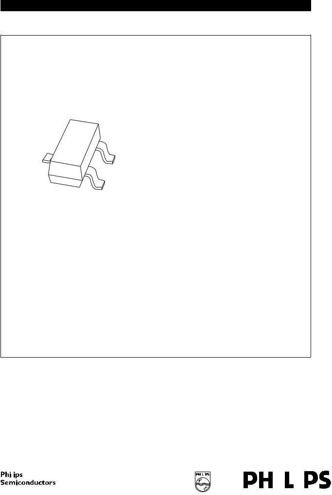
Low-power low noise voltage regulator diodes in small SOT23 plastic SMD packages.
The diodes are available in the normalized E24 ±5% tolerance range. The series consists of 20 types with nominal working voltages from 2.4 to 15 V.
MARKING
PINNING
PIN |
DESCRIPTION |
|
|
1 |
anode |
|
|
2 |
not connected |
|
|
3 |
cathode |
|
|
handbook, halfpage |
1 |
2 |
2
n.c. 1
3
3
Top view |
MAM243 |
Fig.1 Simplified outline (SOT23) and symbol.
TYPE |
MARKING |
TYPE |
MARKING |
TYPE |
MARKING |
TYPE |
MARKING |
NUMBER |
CODE |
NUMBER |
CODE |
NUMBER |
CODE |
NUMBER |
CODE |
|
|
|
|
|
|
|
|
BZX99-C2V4 |
XL |
BZX99-C3V9 |
XS |
BZX99-C6V2 |
XD |
BZX99-C10 |
XX |
|
|
|
|
|
|
|
|
BZX99-C2V7 |
XM |
BZX99-C4V3 |
XT |
BZX99-C6V8 |
XE |
BZX99-C11 |
XY |
|
|
|
|
|
|
|
|
BZX99-C3V0 |
XN |
BZX99-C4V7 |
XA |
BZX99-C7V5 |
XU |
BZX99-C12 |
XZ |
|
|
|
|
|
|
|
|
BZX99-C3V3 |
XP |
BZX99-C5V1 |
XB |
BZX99-C8V2 |
XV |
BZX99-C13 |
X2 |
|
|
|
|
|
|
|
|
BZX99-C3V6 |
XR |
BZX99-C5V6 |
XC |
BZX99-C9V1 |
XW |
BZX99-C15 |
X3 |
|
|
|
|
|
|
|
|
1999 Oct 20 |
2 |

Philips Semiconductors |
|
|
Product specification |
|||
|
|
|
|
|
|
|
Voltage regulator diodes |
|
|
BZX99 series |
|||
|
|
|
|
|
|
|
LIMITING VALUES |
|
|
|
|
|
|
In accordance with the Absolute Maximum Rating System (IEC 134). |
|
|
|
|
||
|
|
|
|
|
|
|
SYMBOL |
PARAMETER |
CONDITIONS |
MIN. |
|
MAX. |
UNIT |
|
|
|
|
|
|
|
IF |
continuous forward current |
|
− |
|
300 |
mA |
IZSM |
non-repetitive peak reverse current |
tp = 100 μs; square wave; |
see Table 1 |
|
||
|
|
Tamb = 25 °C prior to surge |
|
|
|
|
Ptot |
total power dissipation |
Tamb = 25 °C; note 1 |
− |
|
300 |
mW |
Tstg |
storage temperature |
|
−65 |
|
+150 |
°C |
Tj |
junction temperature |
|
− |
|
150 |
°C |
Note
1. Device mounted on an FR4 printed-circuit board.
ELECTRICAL CHARACTERISTICS
Total BZX99-C series
Tj = 25 °C unless otherwise specified.
SYMBOL |
PARAMETER |
CONDITIONS |
MAX. |
UNIT |
|
|
|
|
|
VF |
forward voltage |
IF = 10 mA; see Fig.4 |
0.9 |
V |
|
|
IF = 100 mA; see Fig.4 |
1 |
V |
IR |
reverse current |
|
|
|
|
BZX99-C2V4 |
VR = 1 V |
0.2 |
μA |
|
BZX99-C2V7 |
VR = 1 V |
0.05 |
μA |
|
BZX99-C3V0 |
VR = 1 V |
0.02 |
μA |
|
BZX99-C3V3 |
VR = 2 V |
2 |
μA |
|
BZX99-C3V6 |
VR = 2 V |
1 |
μA |
|
BZX99-C3V9 |
VR = 2 V |
0.5 |
μA |
|
BZX99-C4V3 |
VR = 2 V |
0.1 |
μA |
|
BZX99-C4V7 |
VR = 3 V |
2 |
μA |
|
BZX99-C5V1 |
VR = 3 V |
1 |
μA |
|
BZX99-C5V6 |
VR = 4 V |
1 |
μA |
|
BZX99-C6V2 |
VR = 5 V |
0.1 |
μA |
|
BZX99-C6V8 |
VR = 5 V |
0.01 |
μA |
|
BZX99-C7V5 |
VR = 5 V |
0.1 |
μA |
|
BZX99-C8V2 |
VR = 6 V |
0.2 |
μA |
|
BZX99-C9V1 |
VR = 7 V |
0.1 |
μA |
|
BZX99-C10 |
VR = 7 V |
0.1 |
μA |
|
BZX99-C11 |
VR = 8 V |
0.05 |
μA |
|
BZX99-C12 |
VR = 9 V |
0.05 |
μA |
|
BZX99-C13 |
VR = 10 V |
0.05 |
μA |
|
BZX99-C15 |
VR = 10.5 V |
0.01 |
μA |
1999 Oct 20 |
3 |
 Loading...