


 Loading...
20MHz/40MHz OSCILLOSCOPE
CS-4125A CS-4135A
SERVICE MANUAL
KENWOOD TMI CORPORATION
© 2002-2/B51-1159-00 (K/K)
FILTER |
|
PUSH KNOB |
|
KNOB |
(B11-0540-04) |
|
(K24-3028-03) |
|
(K29-7253-03) |
40MHz OSCILLOSCOPE CS-4135A
MODE |
|
SOURCE |
AUTO NORM FIX TV-F TV-L |
|
VERT CH1 CH2 LINE |
|
ON |
|
|
OFF |
|
CH1 ALT CHOP ADD CH2 |
CH2 INVERT |
SLOPE |
VERT |
ON |
|
MODE |
OFF |
|
CH1 or Y |
|
CH2 or X |
|
|
|
POSITION |
POSITION |
||
2 3 |
|
|
2 3 |
|
VARIABLE |
|
VARIABLE |
|
|
VOLTS / DIV |
VOLTS / DIV |
|||
.2 |
.1 50 |
20 m V |
.2 .1 50 |
20 m V |
.5 |
. |
. 10 |
.5 |
. 10 |
1 |
BAL |
|
BAL |
|
5 |
|
5 |
||
2 |
5 1 |
2 |
1 |
2 |
|
CAL |
CAL |
||
AC |
GND |
DC |
|
DC |
H O R I Z O N T
POSITION
3
SWEEP
ms |
2 1 |
|
5 |
|
|
10 |
|
|
20 |
|
|
50 |
1 |
|
1 |
|
S |
5 |
5 |
|
2 |
|
x 10 MAG |
|
|
|
ON/ |
OFF |
POWER |
CAL |
ILLUM |
FOCUS |
INTEN |
CH2 |
EXT TRIG |
|
|
|
|
CH2 |
||
|
|
|
|
INPUT |
|
INPUT |
|
~ |
|
|
400V |
400V |
42V |
|
1KHz |
|
PK MAX |
MAX |
PK MAX |
|
|
1V p-p ~ |
|
TRACE ROTA CAT 1 1
POWER SWITCH |
|
RUBBER FOOT ; FRONT |
|
KNOB |
|
KNOB |
|
MOLD PANEL |
(S68-0687-05) |
|
(J02-0525-33) |
|
(K29-7255-03) |
|
(Large ; K29-7256-03) |
|
(CS-4125A ; A63-0436-01) |
|
|
|
|
|
|
(Small ; K29-7254-03) |
|
(CS-4135A ; A63-0437-01) |
|
|
|
|
|
||||
|
|
|
|
|
||||
|
|
|
|
|
||||
|
|
|
|
|
|
|
|
|
|
|
|
|
|
|
|
|
|
REAR PANEL (A83-0236-12)
CHI |
Z . AXIS INPUT |
|
OUTPUT |
||
42V˚ PK MAX |
||
|
||
WARNING |
|
TO AVOID ELECTRIC SHOCK THE POWER CORD PROTECTIVE
GROUNDING CONDUCTOR MUST BE CONNECTED TO GROUND.
F O R C O N T I N U E D P R O T E C T I O N A G A I N S T F I R E , R E P L A C E O N L Y
W I T H F U S E O F T H E S P E C I F I E D V O L T A G E A N D C U R R E N T R A T I N G S .
D I S C O N N E C T P O W E R S U P P L Y B E F O R E R E P L A C I N G F U S E .
SELECTOR |
~LINE VOLTAGE FUSE 250V |
|
|
100 |
100V |
T A |
D O N O T |
120 |
120V |
|
R E M O V E C O V E R . |
220 |
220V |
T A |
R E F E R S E R V I C I N G |
230 |
230V |
T O Q U A L I F I E D P E R S O N N E L . |
|
|
|
||
SERIAL
50/60Hz MAX W
KENWOOD TMI CORPORATION
100
230
220


 120
120
RUBBER FOOT ; REAR |
|
AC SELECTOR |
|
CORD WRAP |
(J02-0565-04) |
|
(E68-0619-05) |
|
(W01-0529-08) |
|
|
|
|
|
CS-4125A/CS-4135A
WARNING
The following instructions are for use by qualified personnel only. To avoid electric shock, do not perform any servicing other than contained in the operating instructions unless you are qualified to do so.
|
CONTENTS |
SPECIFICATIONS .......................................................................................................... |
3 |
SAFETY .......................................................................................................................... |
6 |
CIRCUIT DESCRIPTION ................................................................................................ |
7 |
BLOCK DIAGRAM ........................................................................................................ |
10 |
ADJUSTMENT .............................................................................................................. |
12 |
PARTS LIST(UNIT)....................................................................................................... |
20 |
PARTS LIST (ELECTRICAL) ........................................................................................ |
22 |
SCHEMATIC DIAGRAM ............................................................................................... |
48 |
P.C. BOARD ................................................................................................................. |
64 |
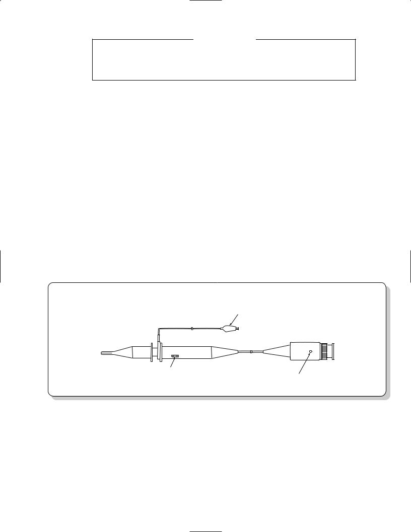
LOW CAPACITY PROBE
Earth clip
PC-54
Atenuation |
Trimmer |
Selector switch |
2

CS-4125A/CS-4135A
SPECIFICATIONS
|
ITE MS |
|
|
|
CS -4125A |
|
CS -4135A |
|
|
|
|
|
|
|
|
CRT |
|
|
|
|
|
|
|
Type |
|
|
|
Rectangular with internal graticule |
|||
Acceleration Voltage |
|
|
|
Approx. 2kV |
|
Approx. 12k V |
|
Display Area |
|
|
|
8 x 10 di v (1 div = 10 m m) |
|||
V E RTICAL AXIS |
(CH1 a nd CH2) |
|
|
|
|||
Sensitivity |
|
|
|
1 mV, 2 mV/div ±5% , 5 mV/div to 5 V /div ±3% |
|||
Attenuator |
|
|
|
1-2-5 step, 12 ranges with fine adjustment |
|||
Input Impedance |
|
|
|
1 MΩ ±2% , Approx. 23 pF |
|||
Frequency Respons e |
|
|
|
|
|||
|
5 mV/div to 5 V /div |
|
DC: DC to 20 M Hz, within –3 dB |
|
DC: DC to 40 M Hz, within –3 dB |
||
|
|
AC: 10 H z to 20 M Hz, within –3 dB |
|
AC: 10 H z to 40 M Hz, within –3 dB |
|||
|
|
|
|
|
|||
|
1 mV/div, 2 mV/div |
|
|
DC: DC to 5 MHz, within –3 dB |
|||
|
|
|
AC: 10 H z to 5 MHz, within –3 dB |
||||
|
|
|
|
|
|||
Rise Time |
|
|
|
|
|
|
|
|
5 mV/div to 5 V /div |
|
|
Approx. 17. 5 ns (20 MHz) |
|
Approx. 8. 75 ns (40 MHz) |
|
|
1 mV/div, 2 mV/div |
|
|
Approx. 70 ns (5 MHz) |
|||
Crosstalk |
|
|
|
-40 dB maximum |
|||
Operating Modes |
|
|
CH1 |
: CH1 signal trance |
|
||
|
|
|
|
CH2 |
: CH2 signal ttrance |
|
|
|
|
|
|
ALT |
: Alternating display of two signals |
|
|
|
|
|
|
CHOP : Chopped display of two signals |
|
||
|
|
|
|
ADD |
: Display of combined C H1 + CH2 waveforms |
||
CHOP Frequency |
|
|
|
A pprox. 250 k Hz |
|||
Channel Polarity |
|
|
|
Normal or inverted, channel 2 only inverted |
|||
|
Maximum Input Voltage |
|
|
800 V peak to peak or 400 V (DC + AC peak) |
|||
|
(peak to peak) |
|
|
|
|||
|
|
|
|
|
|
|
|
|
|
|
|
|
|
||
HORIZO NTAL AXIS |
|
|
|
|
|||
Sensitivity
Input Impedance
Frequency response (-3 dB )
X-YPhase Difference
Operating Modes
Maximum Input Voltage
Same as vertical axis (CH2)
Same as vertical axis (CH2)
DC: DC to 500 k Hz
AC: 10 H z to 500 k Hz
3° or less at 50 kHz
X-Yoperation is selectable with X-Ysetting switch CH1: Y-axis
CH2: X-axis
Same as vertical axis (CH2)
SWEEP SYSTEM
Sweep Modes
Sweep Time
Sweep Magnification
Linearity
NORM: Triggered sweep
AUTO: Auto free run with no signal input
0.5 µs /div to 0. 5 s/div ±3% , |
0.2 µs /div to 0. 5 s/div |
±3% |
(0.2 µs /div: UNCAL) |
|
|
1-2-5 step, 20 r anges with fine adjustment |
|
|
10 x magnification, ±5% |
10 x magnification, |
±5% |
(20 ns/div: UNCAL) |
|
|
±3% (0.2 µs /div: UNCAL) |
±3% , ( ±5% at x 10 MAG) |
|
(±5% at x 10 MAG, 20 ns/div :UNCAL) |
|
|
|
|
|
3

CS-4125A/CS-4135A
SPECIFICATIONS
ITE MS |
|
|
|
|
CS -4125A |
|
|
CS -4135A |
|||
|
|
|
|
|
|
|
|
|
|
|
|
TRIGGERING |
|
|
|
|
|
|
|
|
|
|
|
Triggering Source |
|
|
VERT |
: Input signal selection with VERT MODE control |
|||||||
|
|
|
|
||||||||
|
|
|
|
|
|
|
|
|
|||
|
|
|
|
CH1 |
: CH1 input signal |
|
|
||||
|
|
|
|
|
|
|
|
|
|||
|
|
|
|
CH2 |
: CH2 input signal |
|
|
||||
|
|
|
|
|
|
|
|
|
|||
|
|
|
|
LINE |
: Commercial - use power source |
|
|
||||
|
|
|
|
|
|
|
|
||||
|
|
|
|
EXT |
: Signal input through EXT TRIG terminal |
||||||
|
|
|
|
|
|
|
|
|
|
|
|
External Trigger |
|
|
|
|
|
|
|
|
|
|
|
Input Impedance |
|
|
|
|
|
|
1 MΩ , Approx. 23 pF |
||||
Maximum Input Voltage |
|
|
|
|
84 V peak to peak or 42 V |
(DC + AC peak) |
|||||
Trigger Coupling Modes |
|
|
|
|
|
AUTO, NORM and FIXare capacitively coupled |
|||||
|
|
|
|
|
|
|
|
||||
|
|
|
|
|
TV-F: Vertical sync pulses of a composite video signal |
||||||
|
|
|
|
|
|
|
|
are selected for triggering. |
|||
|
|
|
|
|
TV-L: Horizontal sync pulses of a composite video signal |
||||||
|
|
|
|
|
|
|
|
are selected for triggering. |
|||
Trigger sensitivity |
|
|
|
|
|
|
|
|
|
|
|
CS -4135A |
|
|
|
|
|
|
|
|
|
|
|
MO DE |
|
S IGNAL F RE Q . |
|
|
|
S O URCE |
|||||
|
|
|
V E RT, CH1 , CH2 |
|
E XT |
||||||
|
|
|
|
|
|
|
|
|
|||
NORM |
|
10 Hz to 20 M Hz |
|
|
1.5 div. |
|
0.25 V peak to peak |
||||
|
20 MHz to 40 M Hz |
|
|
2 div. |
|
0.3 V peak to peak |
|||||
|
|
|
|
|
|||||||
AUTO |
|
|
|
|
|
Same as above specs at 50 Hz or above |
|||||
|
|
|
|
|
|
|
|||||
TV-F, TV-L |
|
Composite video Signal |
|
1div. |
|
0.2 V peak to peak |
|||||
|
|
|
|
|
|
|
|
||||
FIX |
|
50 Hz to 40 M Hz |
|
|
2 div. |
|
0.5 V peak to peak |
||||
Trigger sensitivity |
|
|
|
|
|
|
|
|
|
|
|
CS -4125A |
|
|
|
|
|
|
|
|
|
|
|
MO DE |
|
S IGNAL F RE Q . |
|
|
|
S O URCE |
|||||
|
|
|
V E RT, CH1 , CH2 |
|
E XT |
||||||
|
|
|
|
|
|
|
|
|
|||
NORM |
|
10 Hz to 5 MHz |
|
|
1 div. |
|
0.2 V peak to peak |
||||
|
5 MHz to 20 M Hz |
|
|
1.5 div. |
|
0.3 V peak to peak |
|||||
|
|
|
|
|
|||||||
AUTO |
|
|
|
|
|
Same as above specs at 50 Hz or above |
|||||
|
|
|
|
|
|
|
|||||
TV-F, TV-L |
|
Composite video Signal |
|
1div. |
|
0.2 V peak to peak |
|||||
|
|
|
|
|
|
|
|
||||
FIX |
|
50 Hz to 20 M Hz |
|
|
2 div. |
|
0.5 V peak to peak |
||||
4
CS-4125A/CS-4135A
SPECIFICATIONS
ITE MS |
|
CS -4 1 2 5 A |
|
CS -4 1 3 5 A |
|
|
|
|
|
CALIBRATE D S IGNALS |
|
|
|
|
|
|
Positive square wave |
||
|
|
1 V peak to peak |
±3% |
|
Approx. 1 kHz
MO DULATIO N
|
|
|
|
TTL level, decreases brightness |
|
|
|
|
|
Approx. 5 kΩ |
|
|
Usable Frequency Range |
|
DC to 3.5 MHz |
||
|
|
Maximum Input Voltage |
|
84 V peak to peak or 42 V (DC + AC peak) |
|
|
CH1 S IGNAL O UTP UT |
|
|
|
|
|
|
|
|
Approx. 50 mV/div |
(at into 50 Ω load) |
|
|
|
|
Approx. 50 Ω |
|
|
Frequency Response |
|
100 Hz to 10 MHz, ±3 dB |
100 Hz to 20 MHz, ±3 dB |
|
|
|
|
|
(into 50 Ω load) |
(into 50 Ω load) |
|
TRANCE RO TATIO N |
|
|
|
|
|
|
|
|
Adjustable semi-fixed resister on the front panel |
|
|
DIME NS IO NS / WE IGHT ( |
|
) dimensions include protrusion from basic outline dimensions. |
||
|
|
|
|
290 mm (290 mm) |
|
|
|
|
|
150 mm (172 mm) |
|
|
|
|
|
390 mm (443 mm) |
|
|
|
|
|
Approx. 6.6 kg |
Approx. 6.9 kg |
|
E NV IRO NME NTAL |
|
|
|
|
|
Within Specifications |
|
10 to 35 °C / 85% RH or less |
||
|
temp. / hum. range |
|
|||
|
|
|
|
||
|
Full operation temp. / hum. |
|
0 to 40 °C / 85% RH or less |
||
|
range |
|
|||
|
|
|
|
||
|
E NV IRO NME NTAL (Indoor Use O nly) |
|
|||
|
|
|
|
Altitude up to 2000 m |
|
|
|
|
|
OVER VOLTAGE CATEGORY ø |
|
|
|
|
|
POLLUTI ON DEGREE 2 |
|
|
P O WE R S O URCE |
|
|
|
|
|
|
|
|
|
±10% |
|
|
|
|
|
|
|
|
|
|
|
|
|
|
|
|
|
|
|
|
|
|
|
|
5
CS-4125A/CS-4135A
SAFETY
SAFETY
Before connecting the instrument to a power source, carefully read the following information, then verify that the proper power cord is used and the proper line fuse is installed for power source. The specified voltage is shown on the rear panel. If the power cord is not applied for specified voltage, there is always a certain amount of danger from electric shock.
Line voltage
This instrument operates using ac-power input voltages that 100/120/220/230 V at frequencies from 50 Hz to 60Hz.
Power cord
The ground wire of the 3-wire ac power plug places the chassis and housing of the oscilloscope at earth ground. Do not attempt to defeat the ground wire connection or float the oscilloscope ; to do so may pose a great safety hazard. The appropriate power cord is supplied by an option that is specified when the instrument is ordered.
The optional power cords are shown as follows in Fig.1
Line fuse
The fuse holder is located on the rear panel and contains the line fuse. Verify that the proper fuse is installed by replacing the line fuse.
Voltage conversion
This oscilloscope may be operated from either a 100V to 230V, 50/60 Hz power source. Use the following procedure to change from 100 to 230 volt operation or vice versa.
1.Remove the fuse holder.
2.Replace fuse F1 with a fuse of appropriate value, 1 amp for 100 VAC to 120 VAC operation. 630 m amp for 220 VAC to 230 VAC operation.
3.Reinsert it for appropriate voltage range.
4.When performing the reinsertion of fuse holder for the voltage conversion, the appropriate power cord should be used. (See Fig. 1.)
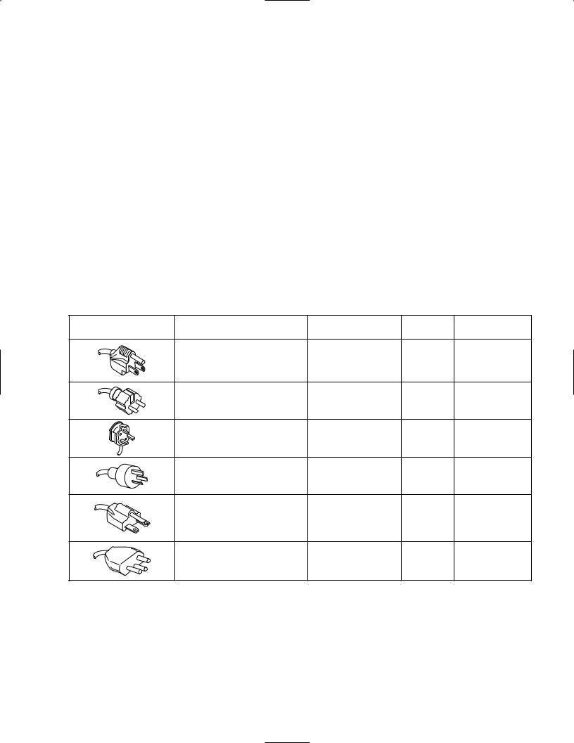
Plug configuration |
power cord and plug type |
Factory installed |
Line cord |
Parts No. for |
|
instrument fuse |
plug fuse |
power cord |
|||
|
|
||||
|
North American |
0.7A, 250V |
|
|
|
|
120 volt/60 Hz |
slow blow |
None |
E30-1951-05 |
|
|
Rated 15 amp |
5x20mm |
|||
|
|
|
|||
|
(12 amp max ; NEC) |
|
|
|
|
|
Universal Europe |
0.3A, 250V |
None |
|
|
|
220 volt/50 Hz |
slow blow |
E30-1952-05 |
||
|
Rated 16 amp |
5x20 mm |
|
|
|
|
U.K. |
0.3A, 250V |
5A |
|
|
|
240 volt/50 Hz |
slow blow |
E30-1963-15 |
||
|
Type C |
||||
|
Rated 5 amp |
5x20 mm |
|
||
|
|
|
|||
|
Australian |
0.3A, 250V |
None |
|
|
|
240 volt/50 Hz |
slow blow |
E30-1953-05 |
||
|
Rated 10 amp |
5x20 mm |
|
|
|
|
North American |
0.3A, 250V |
|
|
|
|
240 volt/60 Hz |
slow blow |
None |
– |
|
|
Rated 15 amp |
5x20mm |
|||
|
|
|
|||
|
(12 amp max ; NEC) |
|
|
|
|
|
Switzerland |
0.3A, 250V |
|
– |
|
|
230 volt/50Hz |
slow blow |
None |
||
|
Rated 10 amp |
5x20 mm |
|
|
Fig.1 Power Input Voltage Configuration
6

CS-4125A/CS-4135A
CIRCUIT DESCRIPTIONS
Vertical Attenuator Circuit
The attenuators of channel 1 and 2 basically consist
of rotary switches and passive elements (resistors, condensers, and trimmer condensers) on PC boards. The resistors have a precision of 0.5% for minimizing any error between the steps of the attenuators.
Vertical input signals from the BNC input receptacle enter the first-stage attenuator circuit, along the path selected by the AC - GND - DC switch. Then they pass through either attenuator 1/1, 1/10, or 1/100, along the path selected by the vertical rotary switch, and become input into the 1st preamplifier (first - stage buffer amplifier).
The 1st preamplifier consists of IC1 (CH2: IC2) hybrid IC. The element used for IC1 features a wide dynamic range and minimized temperature drifting. IC1 functions in the preamplifier as a circuit in which temperature drifting is considered. Input signals, impedance converted in this buffer amplifier, arc sent to the second - stage attenuator where they are passed through either attenuator 1/1, 1/2, 1/4, or 1/10. They are then sent to the vertical amplifier. The second-stage attenuator constitutes a low impedance resistance network with favorable frequency characteristics. The resistors used, as is those of the first stage attenuator, have a precision of 0.5% for minimizing any error between the steps of the attenuators. The rotary switches in this stage include one which increases the gain of the preamplifier to 5- fold when the sensitivity is 1 mV/div or 2 mV/div. IC1 and IC2 have the protection circuit to a large incoming signal.
TC1(51) and TC3(53) are input capacitance regulators for attenuator 1/10 and 1/100, respectively; while TC2(52) and TC4(54) are 1 kHz square wave characteristic regulators for attenuator 1/10 and 1/100. VR1(51) and VR2(52) are step DC balance regulators for attenuators, the former is for user use with adjustment enabled from the front panel.
Vertical Preamplifier Circuit
Signals output from the attenuator circuits are then input into the 2nd preamplifier which consists of a IC3(CH2:IC4) hybrid IC. This IC , with a gain of approximately 12fold , is an amplifier for suppressing DC level temperature drifting. When the sensitivity is either 1 mV/div or 2 mV/div, the gain is further increased another 5-fold(sum of approximately 60-fold) as a result of the gain resistivity of IC3(CH2:IC4) being switched over by the second attenuator switches S1(CH2:IC4) d and e. VR3(53) is the regulator for the DC offset which occurs during this time. Setting the 5 - fold gain is done by a resistor with a 1% precision and a non-regulated operation is achieved. VR4(54) and VR5(55) are 1 kHz square wave characteristic regulators for the sensitivity of 1 mV/div and 10mV/div. TC501(CH2, TC502) are frequency characteristic regulators. Signals which become sufficiently amplified in the 2nd preamplifier pass through the variable circuit of the vertical axis sensitivity, constituted by the volume of the attenuator rotary switch, and then become input into the 3rd amplifier. The 3rd amplifier is a IC5(CH2:IC6) hybrid IC. Signals input into this amplifier become as complementary signals and are output to the 4th amplifier as electric current signals.
The IC contains the CH1(CH2) position circuit, CH2 INV circuit, and CH switch circuit. These are controlled by the CH1(CH2) position volume and CH2 INV switch on the panel unit and the vertical mode switch signals coming from the horizontal side.
VR57 is a sensitivity regulator for CH2 signals while TC6 and TC56 are frequency characteristic regulators for CH1 and CH2, respectively.
CH1(CH2) trigger signals from the 3rd terminal of IC5(CH2:IC6) become amplified in the feedback amplifier in Q16 (19). These trigger signals are converted into electric current signals in Q17 (20) and sent to the trigger source switch on the horizontal side. CH1 trigger signals become amplified between the collector of Q16 and Q18 and in turn become output as CH1 out signals via the emitter follower of Q23. In contrast, CH2 trigger signals become amplified between the collectors in Q19 to Q21, become X - axis signals by being passed through the emitter follower in Q22, converted into electric current signals in VR151 and R182, and in turn output into the horizontal signal switch circuit on the horizontal side. VR151 is the sensitivity regulator of X signals while VR152 is an X position regulator for regulating the DC level of X signals.
The electric current signals which were switched over in the 3rd amplifier are input into the 4th amplifier consisting of Q4 and Q5. After becoming amplified they are directly input into the output amplifier as voltage signals. The 4th amplifier is a feedback amplifier which features minimized fluctuation in the frequency characteristics even when the 3rd amplifiers of CH1 and CH2 are parallel-connected during ADD. Also, the vertical output amplifier can be driven by low output impedance.
Q3 becomes turned on during ADD. The operating current is passed through R103, R104, and VR101 so that the operating current in the 4th amplifier does not become fluctuated when the operating currents from the 3rd amplifiers of CH1 and CH2 flow into the 4th amplifier. VR101 is the ADD balance regulator.
VR102 is the balance regulator of +Y and -Y on the CRT.
Adjustment is made so that the luminescent line comes to the center of the CRT.
Vertical Output Amplifier Circuit
Signals output from the 4th amplifier are amplified about 45 - fold in the output amplifier, Q6 through Q15, and drive the Y deflecting plate of the CRT.
This output amplifier is a feedback amplifier. The final stage Q12 and Q14 are driven by complimentary emitter followers Q8 and Q10, Q9 and Q11, respectively. By doing so, the linearity of the first and last transition high frequencies is improved and the input impedance is made higher. Q13 and Q15 work to obtain sufficient gain during constant current loss in Q12 and Q14, respectively. Negative feedback is sufficiently applied as well. Consequently, this circuit achieves low impedance output of large amplitude signals with good linearity.
VR103 is a sensitivity regulator based on CH1 signals for the entire vertical amplifier. TC101 is a frequency characteristic regulator for the entire vertical amplifier in general and for the output amplifier in particular. VR104
7

CS-4125A/CS-4135A
CIRCUIT DESCRIPTIONS
is the operating point voltage regulator for the output amplifier.
Horizontal System
The horizontal system can be roughly divided into the trigger circuit, sweep circuit, output circuit, and blanking circuit. The TRIG SOURCE switch on the panel unit drives trigger sources switch circuits IC207 (hybrid IC), D202-D205, and Q202. Desired trigger signals can be elected. The trigger source switch circuit is connected to an input buffer for trigger signals from each channel coming from the vertical amplifier, line trigger signals from the power source system, and external synchronizing signals generated in Q201.
Selected synchronizing signals are sent to the trigger level setting circuits Q203 - Q206 and IC202c via the emitter follower in Q203. The trigger level setting circuit constitutes a Schmitt circuit and its threshold level
can be adjusted by |
VOLUME for trigger level setting on |
the panel unit. The |
trigger level becomes fixed voltage |
when the switch in the MODE of a panel side is a fix trigger. VR250 is adjusted so that trigger may start a voltage value in the center of sin wave only at the time of fix.
Selected synchronizing signals are sent to Q207 - Q211 for video - sync separation via C206, Q207, D206 and D207 are polarity switch circuits and Q209 is a sync tip clamper. Q211 is a switch circuit for vertical synchronizing signal separation.
Either ordinary synchronizing signals or video - sync signals become selected at IC202a. IC203a, for MODE switch selecting on the panel unit and the sweep gate flip - flop becomes activated.
Gate signals from IC204b, IC205b turn Q221 ON/OFF in both AUTO and NORM modes and control the sweep HIC in IC201. The interior of IC201 comprises a constant - current charged type ramp wave generating circuit and its time constant becomes determined by an S201 code and C215 or C216. If the S201 code is below 1 ms/div, the time constant adjustment circuit in Q219 becomes activated and VR201 contributes in determining the time constant as well.
If there are no trigger signals during the AUTO mode, the AUTO circuits in Q212-Q215 work and generate sweep gates automatically.
IC201 does not generate ramp waves as the sweep gate become shut by IC205b in the X - Y mode.
Q216 - Q218, Q511, IC205c and IC205d determine the upper limit and hold off time of ramp waves.
Ramp waves from IC201 become output as sweep signals via Q222. Sweep signals and X - axis signals, the latter from the vertical system, become selected by switching circuit Q223, Q224, Q226, and Q227. They are then applied to output systems after Q301.
Horizontal Output Circuit
When horizontal signals are input into Q301 and voltage signals, corresponding to the horizontal position, are input into Q302, differential signals become generated by the collectors in Q307 and Q308, Q309 and Q310. Q303 - Q310 are feedback amplifiers for constant - current load.
They constitute horizontal output amplifiers which feature good linearity and low power consumption. Q315 and Q316 become conductive during X10MAG and increase the horizontal amplifier gain to 10 - fold.
Signals from the horizontal output amplifier are sent to the horizontal deflecting plate of the CRT.
Blanking Circuit
Blanking system circuits generate blanking signals for the CRT and signals which switch each channel in the vertical system. The selected signals are divided into 1/2 in IC204b, which is T - shaped flip - flop connected, and become channel switching signals.
In contrast, signals from the CHOP transmitter and sweep gate negative - phase signals (IC204b Q - signals) are turned into blanking signals in Q230 and IC205a. They are then sent to the blanking amplifier in the power supply system.
Chop Circuit
A CHOP transmitter constitutes IC206a and IC206b. CHOP circuit operates, only when a setup of a panel unit is CHOP sweep.
VERT MODE Circuit
Signals from the CHOP transmitter and sweep gate signals become selected at IC202b, IC203b, whereby CHOP signals are selected during a CHOP operation, while sweep gate signals are selected during an ACT operation. IC204a outputs the change signal of vertical amplifier according to the signal from IC203b, and the state of a setup of a panel unit.
Low Voltage Circuit
[CS-4125A]
The power supply consists of four regulated circuits and two non - regulated circuits. IC1 constitutes an HIC for controlling 4 circuit lines consisting of those for +8 V(Q4, D4), -8 V(Q5, D5), +140 V(Q1, Q2, D3), +5 V(Q3), each voltage becomes determined based on -8 V. VR1 adjusts to -8 V. The +10 V circuits, D6 and C10, are unstable and constitute a power source for the horizontal sweep HIC. The ±10 V generated with D2, C2 and C3 is a non-regulated power which is supplied to high - voltage oscillation circuit and trance rotation circuit. [CS-4135A]
The power supply consists of five regulated circuits and two non-regulated circuits. IC1 constitutes an HIC for controlling 4 circuit lines consisting of those for +8 V(Q4, D4), -8 V(Q5, D5), +140 V(Q1, Q2, D3), +5 V(Q3), each voltage becomes determined based on -8 V. VR1 adjusts to -8V . The +80 V power is generated by Q31 to Q33 using the +8 voltage as the reference. The +10 V circuits, D6 and C10, are unstable and constitute a power source for the horizontal sweep HIC. The ±10 V generated with D2, C2 and C3 is a non-regulated power which is supplied to the scale illumination circuit, highvoltage oscillation circuit and trance rotation circuit.
8

CS-4125A/CS-4135A
CIRCUIT DESCRIPTIONS
High Voltage Blanking Circuit
Q8 oscillates at approximately 50 kHz applying the reactance of the converter transformer. The oscillation voltage appearing in the high voltage coil are turned into stable.
[CS-4125A)
The oscillation voltage appearing in the high-voltage coil are turned into stable -1800 V in the voltage doubler rectifier circuits C25, C26, D9, and D10, and in rectifier circuits Q9 and IC2a.
[CS-4135A]
The oscillation voltage appearing in the high - voltage coil is subjected half - wave rectification then turned into regulated -1500 V by the control circuit formed of Q9 and IC2a.
The voltage across the anode and cathode is about 12 kV. [ both ]
On the secondary side of the converter transformer, there is the coil for the CRT heater for turning the heater on via R52.
Voltage signals, approximately 300 V peak to peak, become extracted from the high voltage coil and used as modulated signals for blanking. This is necessary for employing signals from blanking amplifiers Q15, Q6, and Q7 for the cathode potential.
The modulated signals drive the DC regeneration circuits, D11 - D14, C23 and C24, and provide signals for controlling the brightness of the CRT G1 electrode.
Q10 - 12 are transistors for controlling the focus and they achieve high pressure resistance by being cascade connected.
CAL Circuit
[CS-4125A]
IC71a is a transmitter. Oscillation frequency is decided by surrounding CR. Q71 is the signal outputted from a transmitter, and is the transistor which switch. Output level is decided by voltage of R82, D71, R83, and +140 V when Q71 is OFF.
[CS-4135A]
IC31a is a transmitter. Oscillation frequency is decided by surrounding CR. Q91 is the signal outputted from a transmitter, and is the transistor which switch. Output level is decided by voltage of R72, D91, R73, and +140 V when Q91 is OFF.
Trance Rotation Circuit
This circuit consists of a complementary circuit formed with Q13 and Q14 and drives the rotator coil located on the CRT cone by means of the current from their common emitter.
Scale Illumination Circuit
[CS-4135A]
Q34 and Q35, which are connected in parallel, handles the current flowing through the illumination lamps. They vary the scale illumination VR connected to their common base to control the brightness of the illumination lamps.
9

CS-4135A BLOCK DIAGRAM
|
X65-1500-00 A/2 |
|
|
X80-1550-00 B/4 |
|
|
|
|
|
|
|
|
|
|
|
||
|
|
|
CH2 INVERT |
CH2 |
CH1 |
|
|
X80-1550-00 |
X80-1550-00 A/4 |
|
|
|
|||||
|
(OVERALL UNIT) |
|
POSITION |
POSITION |
|
|
|
|
|
|
|||||||
|
|
S206 |
|
|
C/4 |
|
|
|
|
|
|||||||
|
|
VR205 |
VR204 |
|
|
|
TRACE |
|
|
|
|||||||
|
|
|
|
|
|
|
|
|
|
|
|
|
|
|
|
||
|
|
|
|
|
|
|
|
|
|
|
|
TRACE ROTA |
ROTATION |
ROTATION COIL |
|
||
|
|
|
|
|
|
|
|
|
|
|
|
VR302 |
CIRCUIT |
|
|||
|
|
|
|
|
|
|
|
|
|
|
|
|
|
|
|||
|
|
|
|
|
|
|
|
|
|
|
|
|
Q13,Q14 |
|
|
|
|
|
X65-1500-00 |
|
|
|
|
|
|
|
|
|
|
|
|
|
|
|
|
|
B/2 |
|
|
|
|
|
|
|
|
|
|
|
|
|
|
|
|
|
|
|
INPUT |
|
|
|
|
|
VERTICAL |
|
|
SCALE |
|
|
|
||
CH1 |
AC GND DC |
ATT. |
ATT. |
PRE AMP. |
SELECTOR |
|
ILLUM |
ILLUMINATION |
ILLUM. LAMP |
|
|||||||
BUFFER |
OUT PUT AMP. |
|
|
||||||||||||||
INPUT |
S401 |
S1 first |
S1 second |
IC3 |
|
IC5 |
|
|
VR301 |
CIRCUIT |
|
||||||
IC1 |
|
|
Q3,Q4~Q15 |
|
|
|
|
||||||||||
|
|
|
|
|
|
|
|
|
|
Q34,Q35 |
|
|
|
||||
|
|
|
|
|
|
|
|
|
|
|
|
|
|
|
|
||
|
|
|
|
|
|
|
|
|
TRIG |
CH1 OUT |
|
|
|
|
Vertical |
|
|
|
|
|
|
|
|
|
|
|
OUT PUT AMP. |
|
FOCUS |
|
|
|
|||
|
|
|
|
|
|
|
|
|
BUFFER |
Q18,Q23 |
|
FOCUS |
|
|
|
||
|
|
|
|
|
|
|
|
|
Q16,Q17 |
|
|
CIRCUIT |
|
|
|
||
|
|
|
|
|
|
|
|
|
|
|
VR303 |
Horizontal |
|
||||
|
|
|
|
|
|
|
|
|
|
|
|
Q10! Q12 |
|
||||
|
|
|
INPUT |
|
|
|
|
|
|
|
|
|
|
||||
CH2 |
AC GND DC |
ATT. |
ATT. |
PRE AMP. |
SELECTOR |
|
|
|
|
|
|
|
BLOCK |
||||
BUFFER |
|
|
|
|
|
|
|
||||||||||
INPUT |
S402 |
S2 first |
S2 secound |
IC4 |
|
IC6 |
|
|
|
|
|
|
|
|
|
||
IC2 |
|
|
|
|
|
|
|
|
|
|
|||||||
|
|
|
|
|
|
|
|
|
X-AXIS |
|
|
|
|
H |
|
||
|
|
|
|
|
|
|
|
|
TRIG |
|
|
|
|
|
|||
|
|
|
|
|
|
|
|
|
BUFFER |
|
INTEN |
HIGH VOLTAGE |
H |
|
|||
|
|
|
|
|
|
|
|
|
BUFFER |
Q21,Q22 |
|
|
|||||
|
|
|
|
|
|
|
|
|
|
VR304 |
CIRCUIT |
K |
|
||||
|
|
|
|
|
|
|
|
|
Q19,Q20 |
|
|
|
|||||
|
|
|
|
|
|
CHANNEL |
|
|
|
|
|
IC2a,Q8,Q9 |
|
||||
|
|
|
|
|
|
|
|
|
|
|
|
D11! |
D14,T1 |
G1 |
|
||
|
|
|
|
|
|
CONTROL |
|
|
|
|
|
|
|||||
|
|
|
|
|
|
|
|
|
|
|
|
|
P1 |
|
|||
|
|
|
|
|
|
IC204a,IC206d |
|
|
|
|
|
|
|
CRT |
|||
|
|
|
|
|
|
D218,D219 |
|
|
|
|
|
|
|
|
|
||
|
|
|
|
|
|
|
|
|
INVERT |
|
|
|
VOLTAGE |
|
|
||
|
|
|
|
|
|
|
|
|
|
|
|
DOUBLER |
12kV |
DIAGRAM |
|||
|
|
|
|
|
|
|
|
|
IC206d |
|
|
|
RECTIFIER |
||||
|
|
|
|
|
|
|
|
|
|
|
|
|
|
||||
|
|
|
|
|
|
|
|
|
|
|
|
|
|
A1 |
|
|
|
|
|
|
|
|
CHOP OSC. |
ALT-CHOP |
|
BLANKING |
|
|
BLANKING |
|
|
|
|
||
|
|
|
|
|
IC206a,b,c |
|
|
|
|
|
G2 |
|
|||||
|
|
|
|
|
SELECTOR |
|
SELECTOR |
|
|
|
CRT |
|
|||||
|
|
|
|
|
Q229 |
|
|
|
CIRCUIT |
|
|
||||||
|
|
|
|
|
IC202b |
|
IC205a,Q230 |
|
|
|
|
|
|||||
|
|
|
|
|
|
|
|
|
Q6,Q7,Q15 |
BIAS |
|
X80-1550-00 |
|||||
|
|
|
|
|
|
IC203b |
|
D221,D222 |
|
|
P2 |
||||||
|
|
|
|
|
|
|
|
|
|
VR4,R50,R51 |
|||||||
|
|
|
|
|
|
|
|
|
|
SWEEP TIME |
|
|
|
|
|
D/4 |
|
|
|
|
|
|
|
|
|
|
|
|
|
|
|
|
|
||
|
|
|
|
|
|
|
|
|
|
S201 |
|
|
|
|
|
Z.AXIS INPUT |
|
|
|
|
|
|
|
|
|
|
|
|
|
|
|
|
|
||
|
|
|
|
|
|
|
|
|
|
|
|
|
|
|
|
CH1 |
|
|
|
|
|
|
|
|
|
|
|
|
|
|
|
|
|
OUTPUT |
|
|
|
|
|
TV SYNC. SIGNAL |
|
|
|
|
|
|
|
|
|
|
|
||
|
|
|
|
SEPARATOR |
|
|
|
|
|
|
|
|
|
|
|
||
|
|
|
|
|
|
|
|
|
|
|
|
|
|
|
|
||
|
|
|
|
Q207~Q211 |
|
|
|
|
|
|
HORIZONTAL |
|
|
REFERENCE |
|
|
|
|
|
|
TRIG SOURCE |
D206,D207 |
TRIG MODE |
|
|
|
A SWEEP GATE |
A SWEEP |
HORIZONTAL |
|
|
||||
|
|
|
|
|
|
|
|
SIGNAL |
VOLTAGE |
|
|
||||||
|
SYNC. SIGNAL |
|
SELECTOR |
|
|
SELECTOR |
|
|
|
CIRCUIT |
CIRCUIT |
OUTPUT AMP. |
CAL |
|
|||
EXT TRIG |
|
|
|
|
|
|
SELECTOR |
GENERATOR |
|
||||||||
|
IC207,Q202 |
|
|
IC202a |
|
|
|
IC204b |
IC201 |
Q301~Q310 |
|
||||||
INPUT BUFFER |
|
|
|
|
|
|
Q222~Q224 |
IC31a,Q91 |
|
|
|||||||
INPUT |
|
D202~D205 |
|
|
IC203a |
|
|
|
IC205b |
Q219~Q221 |
Q315,Q316 |
|
|
||||
Q201,Q231 |
|
|
|
|
|
|
Q226~Q227 |
D17,D91 |
|
|
|||||||
|
|
|
TRIG LEVEL |
|
|
AUTO FREE RUN |
|
|
|
|
|
|
|||||
|
|
|
|
|
|
|
|
|
|
|
|
|
|
||||
|
|
|
|
IC202c,d |
|
|
CIRCUIT |
|
|
|
|
|
|
|
|
||
|
|
|
|
Q203~Q206 |
|
|
Q212~Q215 |
|
|
|
|
|
DC |
|
|
||
|
|
|
|
|
|
|
|
|
D210 |
|
|
|
|
|
POWER TRANSFORMER |
|
|
|
|
|
|
|
|
|
|
|
|
HOLD OFF |
|
|
|
|
|
|
|
|
|
|
|
|
|
|
|
|
|
SWEEP END |
|
|
|
|
|
|
|
|
|
|
|
|
|
|
|
|
|
CIRCUIT |
|
|
|
|
|
|
|
|
|
|
|
|
|
|
|
|
|
DETECT |
|
|
|
|
|
|
|
|
|
|
|
|
|
|
|
|
|
IC205c,IC205d |
|
|
|
|
|
|
|
|
|
|
|
|
|
|
|
|
|
Q217 |
|
|
|
|
|
|
|
|
|
|
|
|
|
|
|
|
|
Q216,Q218,Q511 |
|
|
|
LOW VOLTAGE |
|
||
|
|
|
|
|
|
|
|
|
|
|
|
|
|
|
|||
|
|
|
|
|
|
|
|
|
|
|
|
|
|
|
|
||
|
|
|
|
|
|
|
|
|
|
|
|
|
|
|
CIRCUIT |
|
|
|
|
|
|
|
|
|
|
|
|
|
|
|
|
|
IC1,Q1~Q5 |
|
|
|
|
|
|
|
|
|
|
|
|
|
|
|
|
|
Q31~Q33 |
|
|
|
|
|
|
|
|
|
|
|
|
|
|
|
|
|
D1~D6,D31 |
|
|
|
|
|
|
|
|
|
|
|
|
|
|
|
|
|
X80-1550-00 A/4 |
|
|
AC
VERT MODE |
SOURCE |
SLOPE |
TRIGGER |
MODE |
X-Y |
HORIZONTAL |
HORIZONTAL |
" 10 MAG |
POWER SWITCH |
|
LEVEL |
S204,Q201 |
VARIABLE |
POSITION |
& |
||||||
S205 |
S201 |
S203 |
S202,D202 |
S403 |
||||||
VR203 |
D201,D203 |
VR202 |
VR201 |
FUSE |
||||||
|
|
|
|
X65-1500-00 |
||||||
X80-1550-00 B/4 |
|
|
|
|
|
|
|
|
||
|
|
|
|
|
|
|
B/2 |
|
||
|
|
|
|
|
|
|
|
|
10
4135A-4125A/CS-CS
CS-4125A BLOCK DIAGRAM
|
X65-1490-00 A/2 |
|
X80-1540-00 B/4 |
|
|
|
|
|
|
|
|
|
|
|
|
|
|
|||
|
|
|
CH2 INVERT |
|
CH2 |
CH1 |
|
|
|
|
|
|
|
|
|
|
|
|
||
|
(OVERALL UNIT) |
|
POSITION |
POSITION |
|
|
|
|
|
|
|
|
|
|
||||||
|
|
S206 |
|
|
|
|
|
|
|
|
|
|
||||||||
|
|
VR205 |
VR204 |
|
|
|
|
|
|
|
|
|
|
|
||||||
|
X65-1490-00 |
|
|
|
|
|
|
|
|
|
|
|
|
|
|
|
|
|
|
|
|
B/2 |
|
|
|
|
|
|
|
|
|
|
|
|
|
|
|
|
|
|
|
CH1 |
AC GND DC |
ATT. |
INPUT |
ATT. |
PRE AMP. |
|
SELECTOR |
VERTICAL |
|
|
|
|
|
|
|
|
|
|
||
BUFFER |
|
OUT PUT AMP. |
|
|
|
|
|
|
|
|
|
|||||||||
INPUT |
S401 |
S1 first |
S1 second |
IC3 |
|
|
IC5 |
|
|
|
|
|
|
|
|
|
|
|||
IC1 |
|
|
|
Q3,Q4~Q15 |
|
|
|
|
|
|
|
|
|
|
||||||
|
|
|
|
|
|
|
|
|
|
|
X80-1540-00 |
|
X80-1540-00 A/4 |
|
|
|
|
|
||
|
|
|
|
|
|
|
|
|
|
|
|
|
|
|
|
|
|
|
||
|
|
|
|
|
|
|
|
|
|
|
CH1 OUT |
|
C/4 |
|
|
|
|
|
|
|
|
|
|
|
|
|
|
|
|
|
|
|
|
|
TRACE |
|
|
|
|
|
|
|
|
|
|
|
|
|
|
|
|
TRIG |
OUT PUT AMP. |
|
|
|
|
|
|
|
|
|
|
|
|
|
|
|
|
|
|
|
|
TRACE ROTA |
|
ROTATION |
|
|
ROTATION COIL |
|
|||
|
|
|
|
|
|
|
|
|
|
BUFFER |
Q18,Q23 |
|
|
|
|
|
||||
|
|
|
|
|
|
|
|
|
|
|
VR302 |
|
CIRCUIT |
|
|
|
||||
|
|
|
|
|
|
|
|
|
|
Q16,Q17 |
|
|
|
|
|
|
|
|
||
|
|
|
|
|
|
|
|
|
|
|
|
|
|
Q13,Q14 |
|
|
|
|
|
|
|
|
|
|
|
|
|
|
|
|
|
|
|
|
|
|
|
|
|
|
|
CH2 |
AC GND DC |
ATT. |
INPUT |
ATT. |
PRE AMP. |
|
SELECTOR |
|
|
|
|
|
|
|
|
Vertical |
BLOCK |
|||
BUFFER |
|
|
|
|
|
|
|
|
|
|||||||||||
INPUT |
S402 |
S2 first |
S2 secound |
IC4 |
|
|
IC6 |
|
|
|
|
|
|
IC2a,Q8,Q9 |
|
|
||||
IC2 |
|
|
|
|
|
|
|
|
|
|
K |
|
||||||||
|
|
|
|
|
|
|
|
|
|
X-AXIS |
|
|
|
FOCUS |
|
|
|
|
|
|
|
|
|
|
|
|
|
|
|
|
|
|
FOCUS |
|
|
|
|
|
|
||
|
|
|
|
|
|
|
|
|
|
TRIG |
BUFFER |
|
|
CIRCUIT |
|
|
|
|
|
|
|
|
|
|
|
|
|
|
|
|
|
VR303 |
|
|
|
Horizontal |
|
||||
|
|
|
|
|
|
|
|
|
|
BUFFER |
Q21,Q22 |
|
|
Q10~Q12 |
|
|
|
|||
|
|
|
|
|
|
|
|
|
|
|
|
|
|
|
|
|||||
|
|
|
|
|
|
|
CHANNEL |
|
Q19,Q20 |
|
|
|
|
|
|
|
|
|
|
|
|
|
|
|
|
|
|
|
|
|
|
|
|
|
|
|
|
|
|
||
|
|
|
|
|
|
|
CONTROL |
|
|
|
|
|
|
|
|
|
H |
|
|
|
|
|
|
|
|
|
|
IC204a,IC206d |
|
|
|
|
|
|
|
|
|
CRT |
|
||
|
|
|
|
|
|
|
D218,D219 |
|
|
|
|
|
INTEN |
|
HIGH VOLTAGE |
|
|
H |
|
|
|
|
|
|
|
|
|
|
|
|
|
|
|
VR304 |
|
CIRCUIT |
|
|
|
|
|
|
|
|
|
SEPARATOR |
|
|
|
|
INVERT |
|
|
|
|
D11~D14,T1 |
|
|
G1 |
|
DIAGRAM |
|
|
|
|
|
|
|
|
|
IC206d |
|
|
|
|
|
|
|
P1 |
|
|||
|
|
|
|
|
|
|
|
|
|
|
|
|
|
|
|
|
|
|
||
|
|
|
|
|
|
|
|
|
|
|
|
|
|
|
|
|
|
|
|
|
|
|
|
|
|
CHOP OSC. |
|
ALT-CHOP |
|
BLANKING |
|
|
|
|
|
|
|
|
|
|
|
|
|
|
|
|
IC206a,b,c |
|
|
|
|
BLANKING |
|
|
|
|
G2 |
|
|
|||
|
|
|
|
|
|
SELECTOR |
|
SELECTOR |
|
|
|
|
|
|
|
|
||||
|
|
|
|
|
Q229 |
|
|
|
|
CIRCUIT |
|
CRT |
|
|
|
|
||||
|
|
|
|
|
|
IC202b |
IC205a,Q230 |
|
|
|
|
|
|
X80-1540-00 |
|
|||||
|
|
|
|
|
|
|
|
|
Q6,Q7,Q15 |
|
BIAS |
|
|
|
|
|||||
|
|
|
|
|
|
|
IC203b |
|
D221,D222 |
|
|
|
|
|
P2 |
|
||||
|
|
|
|
|
|
|
|
|
|
|
|
VR4,R50,R51 |
|
|
D/4 |
|
||||
|
|
|
|
|
|
|
|
|
|
|
|
|
|
|
|
|
|
|||
|
|
|
|
|
|
|
|
|
|
|
SWEEP TIME |
|
|
|
|
|
|
|
|
|
|
|
|
|
|
|
|
|
|
|
|
S201 |
|
|
|
|
|
|
|
Z.AXIS INPUT |
|
|
|
|
|
|
|
|
|
|
|
|
|
|
|
|
|
|
|
|
|
|
|
|
|
|
|
|
|
|
|
|
|
|
|
|
|
|
|
|
|
CH1 |
|
|
|
|
|
|
|
|
|
|
|
|
|
|
|
|
|
|
|
|
OUTPUT |
|
|
|
|
|
TV SYNC. SIGNAL |
|
|
|
|
|
|
|
|
|
|
|
|
|
|
|
|
|
|
|
|
Q207~Q211 |
|
|
|
|
|
|
|
|
|
|
|
|
|
|
|
|
|
|
|
TRIG SOURCE |
D206,D207 |
TRIG MODE |
|
|
A SWEEP GATE |
A SWEEP |
HORIZONTAL |
HORIZONTAL |
|
REFERENCE |
|
|
|||||
|
|
|
|
|
|
|
SIGNAL |
|
|
VOLTAGE |
|
|
||||||||
|
|
|
SELECTOR |
|
|
SELECTOR |
|
|
|
CIRCUIT |
CIRCUIT |
|
OUTPUT AMP. |
|
|
|
||||
|
SYNC. SIGNAL |
|
|
|
|
|
|
SELECTOR |
|
GENERATOR |
CAL |
|
||||||||
EXT TRIG |
|
IC207,Q202 |
|
|
|
IC202a |
|
|
|
IC204b |
IC201 |
Q301~Q310 |
|
|
|
|||||
INPUT BUFFER |
|
|
|
|
|
|
|
Q222~Q224 |
|
|
IC71a,Q71 |
|
|
|||||||
INPUT |
|
D202~D205 |
|
|
|
IC203a |
|
|
|
IC205b |
Q219~Q221 |
Q315,Q316 |
|
|
|
|
||||
Q201,Q231 |
|
|
|
|
|
|
|
Q226~Q227 |
|
|
D17,D71 |
|
|
|||||||
|
|
|
TRIG LEVEL |
|
|
AUTO FREE RUN |
|
|
|
|
|
|
|
|||||||
|
|
|
|
|
|
|
|
|
|
|
|
|
|
|
|
|||||
|
|
|
|
IC202c,d |
|
|
|
|
CIRCUIT |
|
|
|
|
|
|
|
|
|
|
|
|
|
|
|
Q203~Q206 |
|
|
|
Q212~Q215 |
|
|
|
|
|
|
|
DC |
|
|
||
|
|
|
|
|
|
|
|
|
|
D210 |
|
|
|
|
|
|
|
POWER TRANSFORMER |
|
|
|
|
|
|
|
|
|
|
|
|
|
HOLD OFF |
|
|
|
|
|
|
|
|
|
|
|
|
|
|
|
|
|
|
|
|
SWEEP END |
|
|
|
|
|
|
|
|
|
|
|
|
|
|
|
|
|
|
|
|
CIRCUIT |
|
|
|
|
|
|
|
|
|
|
|
|
|
|
|
|
|
|
|
|
DETECT |
|
|
|
|
|
|
|
|
|
|
|
|
|
|
|
|
|
|
|
IC205c,IC205d |
|
|
|
|
|
|
|
|
||
|
|
|
|
|
|
|
|
|
|
Q217 |
|
|
|
|
|
|
|
|
||
|
|
|
|
|
|
|
|
|
|
Q216,Q218,Q511 |
|
|
|
|
|
|
|
|
||
|
|
|
|
|
|
|
|
|
|
|
|
|
|
|
|
LOW VOLTAGE |
|
|
||
|
|
|
|
|
|
|
|
|
|
|
|
|
|
|
|
|
|
|
|
|
|
|
|
|
|
|
|
|
|
|
|
|
|
|
|
|
|
|
CIRCUIT |
|
|
|
|
|
|
|
|
|
|
|
|
|
|
|
|
|
|
|
|
IC1,Q1~Q5 |
|
|
|
|
|
|
|
|
|
|
|
|
|
|
|
|
|
|
|
|
D1~D6 |
|
|
|
|
|
|
|
|
|
|
|
|
|
|
|
|
|
|
|
|
X80-1540-00 A/4 |
|
|
|
VERT MODE |
SOURCE |
SLOPE |
TRIGGER |
MODE |
|
X-Y |
|
|
HORIZONTAL |
HORIZONTAL |
" 10 MAG |
|
POWER SWITCH |
|
|||||
|
LEVEL |
|
|
S204,Q201 |
|
|
VARIABLE |
POSITION |
|
& |
|
|||||||||
|
|
S205 |
S201 |
S203 |
S202,D202 |
|
|
|
S403 |
|
|
|||||||||
|
|
VR203 |
D201,D203 |
|
|
VR202 |
VR201 |
|
|
FUSE |
|
|||||||||
|
|
|
|
|
|
|
|
|
|
|
|
|
|
|||||||
X80-1540-00 B/4 |
X65-1490-00 |
|
B/2 |
||
|
11
4135A-4125A/CS-CS

CS-4125A/CS-4135A
ADJUSTMENT
To obtain the best performance, periodically calibrate the unit. Sometimes, only one mode need be calibrated, while at other times, all modes should be calibrated. When one mode is calibrated, it must be noted that the other modes may be affected. When calibrating all modes, perform the calibration in the specified sequence.
The following calibration required an accurate measuring instrument and an insulated adjusting flat blade screwdriver. If they are not available, contact your dealer. For optimum adjustment, turn the power on and warm up the scope sufficiently (more than 30 minutes) before starting. Before calibrating the scope, check the power supply voltage.
TEST EQUIPMENT REQUIRED
The following instrument or their equivalent should be used for making adjustment.
Test Equipment |
Model |
|
Digital Multi Meter |
45 |
|
(FLUKE) |
||
|
||
Pulse generator |
PG-506 |
|
(Tektronix) |
||
|
||
Time Marker |
TG-501 |
|
(Tektronix) |
||
|
||
Sine-wave Generator (1) |
SG-503 |
|
(Tektronix) |
||
|
||
Sine-wave Generator (2) |
SG-502 |
|
(Tektronix) |
||
|
||
Square Wave Generator |
211B |
|
(HP) |
||
|
||
Capacitance meter |
3520 |
|
(HIOKI) |
||
|
||
Oscilloscope |
2465B |
|
(Tektronix) |
||
|
||
Pattern generator |
CG-911 |
|
(KENWOOD TMI) |
||
|
||
Frequency counter |
FC-756 |
|
(KENWOOD TMI) |
||
|
||
CASE JIG |
CASE JIGU 20M |
|
(KENWOOD TMI or H/C) |
||
|
PREPARATION FOR ADJUSTMENT
Control Settings
The control settings listed below must be used for each adjustment procedure.
Exceptions to these settings will be noted as they occur. After completing a adjustment, return the controls to the following setting.
NAME OF KNOBS |
POSITION |
MODE |
AUTO |
X-Y |
OFF |
SOURCE |
VERT |
VERT MODE |
CH1 |
CH2 INVERT |
OFF |
SLOPE |
OFF (+) |
TRIGGER LEVEL |
12 O’clock |
V.POSITION |
12 O’clock (both CH1, |
|
2) |
VOLTS/DIV |
10mV (both CH1, 2) |
VOLTS VARIABLE |
CAL (both CH1, 2) |
AC-GND-DC |
DC (both CH1, 2) |
H. POSITION |
12 O’clock |
SWEEP TIME VARIABLE |
CAL |
SWEEP TIME/DIV |
0.1ms |
SWEEP TIME/DIV MAG |
OFF |
(x10) |
|
12

|
|
|
|
|
|
CS-4125A/CS-4135A |
||||||
|
|
|
|
ADJUSTMENT |
|
|
|
|
||||
|
|
|
|
|
|
|
|
|
|
|
|
|
|
Item |
|
Adjustment |
|
|
|
|
|
Procedure |
|
||
|
|
point |
|
|
|
|
|
|
||||
|
|
|
|
|
|
|
|
|
|
|
|
|
|
|
|
|
|
|
|
|
|
|
|
|
|
|
-8 V |
|
VR1 |
|
|
[CS-4125A] |
|
|
|
|
||
|
|
|
[CS-4125A] |
|
|
The probe of multi-meter is applied to the CN8-4 (20M) of a power |
|
|||||
|
|
|
X80-1540 |
|
|
supply unit, and it adjusts so that it may be set to –8.00 V. |
|
|||||
|
|
|
[CS-4135A] |
|
|
|
|
|
|
|
|
|
1 |
|
|
X80-1550 |
|
|
[CS-4135A] |
|
|
|
|
||
|
|
|
|
|
|
The probe of multi-meter is applied to the CN11-6 (40 M) of a power |
|
|||||
|
|
|
|
|
|
supply unit, and it adjusts so that it may be set to –8.00 V. |
|
|||||
|
|
|
|
|
|
Adjustment range: -8.00 V to –8.05 V |
|
|||||
|
|
|
|
|
|
|
|
|
|
|
|
|
|
CRT center |
|
VR102 |
|
|
|
|
|
|
|
|
|
|
|
|
|
MODE : AUTO |
VOLTS/DIV : 50mV (both CH) |
|
|
|||||
|
|
|
[CS-4125A] |
|
|
|
|
|||||
|
|
|
|
|
VERT MODE : CH2 |
VOLTS VARIABLE : CAL (both CH) |
|
|
||||
|
|
|
X65-1490 |
|
|
|
|
|||||
|
|
|
|
|
AC-GND-DC : GND |
|
|
|
|
|||
2 |
|
|
[CS-4135A] |
|
|
|
|
|
|
|||
|
|
X65-1500 |
|
|
1) CH2 INVERT is turned ON-OFF and the position which |
|
||||||
|
|
|
|
|
|
|||||||
|
|
|
|
|
|
luminescent line does not move is looked for by CH2 POSITION. |
|
|||||
|
|
|
|
|
|
2) CH2 POSITION leaves as it is and adjusts luminescent line in the |
|
|||||
|
|
|
|
|
|
scale center of CRT by VR102. |
|
|||||
|
Operating point |
voltage |
VR104 |
|
|
[CS-4125A] |
|
|
|
|
||
|
of vertical amplifier |
[CS-4125A] |
|
|
Adjust luminescent line to a CRT center. |
|
||||||
|
|
|
X65-1490 |
|
|
In the state of two clauses, a main part is adjusted by VR104 so that |
|
|||||
|
|
|
[CS-4135A] |
|
|
the voltage of CN6-1 may be set to 67.00 V. |
|
|||||
|
|
|
X65-1500 |
|
|
[CS-4135A] |
|
|
|
|
||
|
|
|
|
|
|
Adjust luminescent line to a CRT center. |
|
|||||
3 |
|
|
|
|
|
In the state of two clauses, a main part is adjusted by VR104 so that |
|
|||||
|
|
|
|
|
|
the voltage of CN6-1 may be set to 37.50 V. |
|
|||||
|
|
|
|
|
|
Adjustment range: [CS-4125A] 66.95 V to 67.05 V |
|
|||||
|
|
|
|
|
|
|
[CS-4135A] 37.45 V to 37.55 V |
|
||||
|
|
|
|
|
|
*1. Carry out and adjust SWEEP TIME to 1ms in the state of sweep. |
|
|||||
|
|
|
|
|
|
*2. Make it short-circuit, measure and adjust CN6-1 and 4. |
|
|||||
|
Operating point |
voltage |
VR301 |
|
|
|
|
|
|
|
|
|
|
|
|
MODE : AUTO |
VOLTS/DIV : 50 mV (both CH) |
|
|
||||||
|
of horizontal amplifier |
[CS-4125A] |
|
|
|
|
||||||
|
|
|
VERT MODE : CH1 |
X-Y : ON |
|
|
||||||
|
|
|
X65-1490 |
|
|
|
|
|||||
|
|
|
|
|
AC-GND-DC : GND |
|
|
|
|
|||
|
|
|
[CS-4135A] |
|
|
|
|
|
|
|||
|
|
|
|
|
|
|
|
|
|
|
|
|
4 |
|
|
X65-1500 |
|
|
1) Move the spot to the CRT center by operating the H.POSITION |
|
|||||
|
|
|
|
|
controls. |
|
|
|
|
|||
|
|
|
|
|
|
|
|
|
|
|||
|
|
|
|
|
|
2) It adjusts by VR301 so that the voltage of CN7-1 may be set to |
|
|||||
|
|
|
|
|
|
68.00 V. |
|
|
|
|
||
|
|
|
|
|
|
Adjustment range: 67.95 V to 68.05 V |
|
|||||
|
|
|
|
|
|
* Make it short-circuit, measure and adjustment CN7-1 and 3. |
|
|||||
|
ASTIG |
|
VR4 |
|
|
|
|
|
|
|
|
|
|
|
|
|
FOUCUS : 12 o’clock |
X-Y : ON |
|
|
|||||
|
|
|
[CS-4125A] |
|
|
|
|
|||||
|
|
|
|
|
|
|
|
|
|
|
|
|
|
|
|
X80-1540 |
|
|
A FOUCUS knob is the state at 12:00 position, and it adjusted by |
|
|||||
5 |
|
|
[CS-4135A] |
|
|
VR4 so that it may become the smallest about spot. |
|
|||||
|
|
X80-1550 |
|
|
NG |
|
NG |
|
||||
|
|
|
|
|
|
|
||||||
|
|
|
|
|
|
|
|
|
|
|
|
|
|
|
|
|
|
|
|
Best point |
|
||||
|
|
|
|
|
|
|
|
|
|
|
|
|
|
FOUCUS center |
|
VR3 |
|
|
|
|
|
|
|
|
|
|
|
|
|
FOUCUS : 12 o’clock |
X-Y : ON |
|
|
|||||
|
|
|
[CS-4125A] |
|
|
|
|
|||||
|
|
|
|
|
|
|
|
|
|
|
|
|
6 |
|
|
X80-1540 |
|
|
A FOUCUS knob is the state at 12:00 position, and it adjusted by |
|
|||||
|
|
|
[CS-4135A] |
|
|
VR3 so that it may become the smallest about spot. |
|
|||||
|
|
|
X80-1550 |
|
|
|
|
|
|
|
|
|
|
|
|
|
|
|
|
|
|
|
|
|
|
13

|
|
|
|
CS-4125A/CS-4135A |
||||||||||||||||||||||
|
|
|
ADJUSTMENT |
|
|
|
|
|
|
|
|
|
|
|
|
|
|
|
||||||||
|
|
|
|
|
|
|
|
|
|
|
|
|
|
|
|
|
|
|
|
|
|
|
|
|
|
|
|
Item |
Adjustment |
|
|
|
|
|
|
|
|
|
Procedure |
|
|
|
|
|
|
|
|||||||
|
point |
|
|
|
|
|
|
|
|
|
|
|
|
|
|
|
|
|||||||||
|
|
|
|
|
|
|
|
|
|
|
|
|
|
|
|
|
|
|
|
|
|
|
|
|
|
|
|
|
|
|
|
|
|
|
|
|
|
|
|
|
|
|
|
|
|
|
|
|
|
|
|
|
|
|
INTEN |
VR2 |
|
X-Y: ON |
|
|
|
|
|
|
|
|
|
|
|
|
|
|
|
|||||||
|
|
CS-4125A] |
|
|
|
|
|
|
|
|
|
|
|
|
|
|
|
|
||||||||
|
|
|
|
|
|
|
|
|
|
|
|
|
|
|
|
|
|
|
|
|
|
|
|
|
|
|
7 |
|
X80-1540 |
|
1) Spot is displayed on CRT and INTEN knob is made the position at |
|
|||||||||||||||||||||
|
|
[CS-4135A] |
|
9:00. |
|
|
|
|
|
|
|
|
|
|
|
|
|
|
|
|
|
|
|
|
||
|
|
X80-1550 |
|
2) Adjust VR2 so that spot may disappear in the position at 9:00. |
|
|||||||||||||||||||||
|
CH1 STEP ATT |
VR2 |
|
|
|
|
|
|
|
|
|
|
|
|
|
|
|
|
|
|
|
|
|
|
|
|
|
|
MODE : AUTO |
AC-GND-DC : GND |
|
|
|
|
|
|
|
||||||||||||||||
|
BALANCE |
[CS-4125A] |
|
|
|
|
|
|
|
|
||||||||||||||||
|
|
VERT MODE : CH1 |
V OLTS/DIV : 2 mV |
|
|
|
|
|
|
|
||||||||||||||||
|
(CH1 1 mV to 2 mV) |
X65-1490 |
|
|
|
|
|
|
|
|
||||||||||||||||
|
|
|
|
|
|
|
|
|
|
|
|
|
|
|
|
|
|
|
|
|
|
|
|
|
||
8 |
|
[CS-4135A] |
|
Adjust VR2 so that the luminescent line does not move when VOLTS |
|
|||||||||||||||||||||
|
|
X65-1500 |
|
is switched from 1 mV to 2 mV. |
|
|
|
|
|
|
|
|||||||||||||||
|
|
|
|
* On the basis of 2 mV, it adjusts at the 1 mV time. |
|
|
|
|
|
|
|
|||||||||||||||
|
|
|
|
* CH1 STEP ATT BALANCE VR is united with a center. (mechanical) |
|
|||||||||||||||||||||
|
CH1 STEP ATT |
VR3 |
|
|
|
|
|
|
|
|
|
|
|
|
|
|
|
|
|
|
|
|
|
|
|
|
|
|
MODE : AUTO |
AC-GND-DC : GND |
|
|
|
|
|
|
|
||||||||||||||||
|
BALANCE |
[CS-4125A] |
|
|
|
|
|
|
|
|
||||||||||||||||
|
|
VERT MODE : CH1 |
VOLTS/DIV : 5 mV |
|
|
|
|
|
|
|
||||||||||||||||
|
(CH1 2 mV to 5 mV) |
X65-1490 |
|
|
|
|
|
|
|
|
||||||||||||||||
|
|
|
|
|
|
|
|
|
|
|
|
|
|
|
|
|
|
|
|
|
|
|
|
|
||
9 |
|
[CS-4135A] |
|
Adjust VR3 so that the luminescent line does not move when VOLTS |
|
|||||||||||||||||||||
|
|
X65-1500 |
|
is switched from 2 mV to 5mV. |
|
|
|
|
|
|
|
|||||||||||||||
|
|
|
|
* On the basis of 5 mV, it adjusts at the 2 mV time. |
|
|
|
|
|
|
|
|||||||||||||||
|
|
|
|
* Don’t touch CH1 STEP ATT BALANCE VR performed by 8 clauses. |
|
|||||||||||||||||||||
|
CH2 STEP ATT |
VR52 |
|
|
|
|
|
|
|
|
|
|
|
|
|
|
|
|
|
|
|
|
|
|
|
|
|
|
MODE : AUTO |
AC-GND-DC : GND |
|
|
|
|
|
|
|
||||||||||||||||
|
BALANCE |
[CS-4125A] |
|
|
|
|
|
|
|
|
||||||||||||||||
|
|
VERT MODE : CH2 |
VOLTS/DIV : 2 mV |
|
|
|
|
|
|
|
||||||||||||||||
|
(CH2 1 mV to 2mV) |
X65-1490 |
|
|
|
|
|
|
|
|
||||||||||||||||
|
|
|
|
|
|
|
|
|
|
|
|
|
|
|
|
|
|
|
|
|
|
|
|
|
||
10 |
|
[CS-4135A] |
|
Adjust VR52 so that the luminescent line does not move when |
|
|
||||||||||||||||||||
|
|
X65-1500 |
|
VOLTS is switched from 1 mV to 2 mV. |
|
|
|
|
|
|
|
|||||||||||||||
|
|
|
|
* On the basis of 2 mV, it adjusts at the 1 mV time. |
|
|
|
|
|
|
|
|||||||||||||||
|
|
|
|
* CH2 STEP ATT BALANCE VR is united with a center. (mechanical) |
|
|||||||||||||||||||||
|
CH2 STEP ATT |
VR53 |
|
|
|
|
|
|
|
|
|
|
|
|
|
|
|
|
|
|
|
|
|
|
|
|
|
|
MODE : AUTO |
AC-GND-DC : GND |
|
|
|
|
|
|
|
||||||||||||||||
|
BALANCE |
[CS-4125A] |
|
|
|
|
|
|
|
|
||||||||||||||||
|
|
VERT MODE : CH2 |
VOLTS/DIV : 5 mV |
|
|
|
|
|
|
|
||||||||||||||||
|
(CH2 2mV to 5 mV) |
X65-1490 |
|
|
|
|
|
|
|
|
||||||||||||||||
|
|
|
|
|
|
|
|
|
|
|
|
|
|
|
|
|
|
|
|
|
|
|
|
|
||
11 |
|
[CS-4135A] |
|
Adjust VR53 so that the |
luminescent line does |
not move when |
|
|||||||||||||||||||
|
X65-1500 |
|
VOLTS is switched from 2 mV to 5 mV. |
|
|
|
|
|
|
|
||||||||||||||||
|
|
|
|
|
|
|
|
|
|
|||||||||||||||||
|
|
|
|
* On the basis of 5 mV, it adjusts at the 2 mV time. |
|
|
|
|
|
|
|
|||||||||||||||
|
|
|
|
* Don’t touch VR of CH2 STEP ATT BALANCE performed by 10 |
|
|||||||||||||||||||||
|
|
|
|
clauses. |
|
|
|
|
|
|
|
|
|
|
|
|
|
|
|
|||||||
|
ADD POSI |
VR101 |
|
|
|
|
|
|
|
|
|
|
|
|
|
|
|
|
|
|
|
|
|
|
|
|
|
|
MODE : AUTO |
AC-GND-DC : GND (both CH) |
|
|
|||||||||||||||||||||
|
|
[CS-4125A] |
|
|
|
|||||||||||||||||||||
|
|
|
VERT MODE : ALT |
VOLTS/DIV : 10 mV (both CH) |
|
|
||||||||||||||||||||
|
|
X65-1490 |
|
|
|
|||||||||||||||||||||
|
|
|
|
|
|
|
|
|
|
|
|
|
|
|
|
|
|
|
|
|
|
|
|
|
|
|
12 |
|
[CS-4135A] |
|
1) In the state of ALT, luminescent line of CH1 and CH2 is united in |
|
|||||||||||||||||||||
|
|
X65-1500 |
|
the center of CRT by V. POSITION. |
|
|
|
|
|
|
|
|||||||||||||||
|
|
|
|
2) VERT MODE is switched to ADD, and it adjusts by VR101 so that |
|
|||||||||||||||||||||
|
|
|
|
luminescent line may become in the center. |
|
|
|
|
|
|
|
|||||||||||||||
|
CH1 10 mV, 1 mV |
10 mV: VR5 |
|
|
|
|
|
|
|
|
|
|
|
|
|
|
|
|
|
|
|
|
|
|
|
|
|
|
MODE : AUTO |
AC-GND-DC : DC |
|
|
|
|
|
|
|
||||||||||||||||
|
Square wave |
1 mV: VR4 |
|
|
|
|
|
|
|
|
||||||||||||||||
|
|
VERT MODE : CH1 |
VOLTS/DIV : 10 mV, 1 mV |
|
|
|||||||||||||||||||||
|
|
[CS-4125A] |
|
|
|
|||||||||||||||||||||
|
|
|
SWEEP TIME : 0.5 ms |
|
|
|
|
|
|
|
|
|
|
|
|
|
|
|
||||||||
|
|
X65-1490 |
|
|
|
|
|
|
|
|
|
|
|
|
|
|
|
|
||||||||
|
|
|
|
|
|
|
|
|
|
|
|
|
|
|
|
|
|
|
|
|
|
|
|
|
|
|
|
|
[CS-4135A] |
|
1) Input a 1 kHz square wave signal to the CH1 INPUT (6 div. input) |
|
|||||||||||||||||||||
13 |
|
X65-1500 |
|
2) Adjust each VR so that the waveform is flat. |
|
|
|
|
|
|
|
|||||||||||||||
|
|
|
|
|
|
NG |
OK |
|
NG |
|
||||||||||||||||
|
|
|
|
|
|
|
|
|
||||||||||||||||||
|
|
|
|
|
|
|
|
|
|
|
|
|
|
|
|
|
|
|
|
|
|
|
|
|
|
|
|
|
|
|
|
|
|
|
|
|
|
|
|
|
|
|
6 div. |
|
|
|
|
|
|
|
|
||
|
|
|
|
|
|
|
|
|
|
|
|
|
|
|
|
|
|
|
|
|
|
|
|
|
|
|
|
|
|
|
|
|
|
|
|
|
|
|
|
|
|
|
|
|
|
|
|
|
|
|
|
|
|
|
|
|
|
|
|
|
|
|
|
|
|
|
|
|
|
|
|
|
|
|
|
|
|
|
|
|
14

|
|
|
|
|
CS-4125A/CS-4135A |
||||||||||||||||||||||||||||||||
|
|
ADJUSTMENT |
|
|
|
|
|
|
|
|
|
|
|
|
|
|
|
|
|
|
|
||||||||||||||||
|
|
|
|
|
|
|
|
|
|
|
|
|
|
|
|
|
|
|
|
|
|
|
|
|
|
|
|
|
|
|
|
|
|
|
|
|
|
|
Item |
Adjustment |
|
|
|
|
|
|
|
|
|
|
|
|
|
|
|
|
|
|
Procedure |
|
|
|
|
|
|
|
|||||||||
|
point |
|
|
|
|
|
|
|
|
|
|
|
|
|
|
|
|
|
|
|
|
|
|
|
|
|
|||||||||||
|
|
|
|
|
|
|
|
|
|
|
|
|
|
|
|
|
|
|
|
|
|
|
|
|
|
|
|
|
|
|
|
|
|
|
|
|
|
|
CH2 10 mV, 1 mV |
10 mV: VR55 |
|
|
|
|
|
|
|
|
|
|
|
|
|
|
|
|
|
|
|
|
|
|
|
|
|
|
|
|
|
|
|
|
|
|
|
|
|
|
MODE : AUTO |
|
|
AC-GND-DC : DC |
|
|
|
|
|
|
|
||||||||||||||||||||||||
|
Square wave |
1 mV: VR54 |
|
|
|
|
|
|
|
|
|
|
|
||||||||||||||||||||||||
|
|
|
VERT MODE : CH2 |
|
|
VOLTS/DIV : 10 mV, 1 mV |
|
|
|||||||||||||||||||||||||||||
|
|
[CS-4125A] |
|
|
|
|
|
|
|||||||||||||||||||||||||||||
|
|
|
|
SWEEP TIME : 0.5 ms |
|
|
|
|
|
|
|
|
|
|
|
|
|
|
|
|
|
|
|
||||||||||||||
|
|
X65-1490 |
|
|
|
|
|
|
|
|
|
|
|
|
|
|
|
|
|
|
|
|
|
||||||||||||||
|
|
|
|
|
|
|
|
|
|
|
|
|
|
|
|
|
|
|
|
|
|
|
|
|
|
|
|
|
|
|
|
|
|
|
|
|
|
|
|
|
|
|
|
|
|
|
|
|
|
|
|
|
|
|
|
|
|
|
|
|
|
|
|
|
|
|
|
|
|
|
|
|
|
|
|
|
|
[CS-4135A] |
|
1) Input a 1 kHz square wave signal to the CH2 INPUT. (6 div. input) |
|
||||||||||||||||||||||||||||||||
14 |
|
X65-1500 |
|
2) Adjust each VR so that the waveform is flat. |
|
|
|
|
|
|
|
||||||||||||||||||||||||||
|
|
|
|
|
|
|
|
|
NG |
|
OK |
NG |
|
||||||||||||||||||||||||
|
|
|
|
|
|
|
|
|
|
|
|
||||||||||||||||||||||||||
|
|
|
|
|
|
|
|
|
|
|
|
|
|
|
|
|
|
|
|
|
|
|
|
|
|
|
|
|
|
|
|
|
|
|
|
|
|
|
|
|
|
|
|
|
|
|
|
|
|
|
|
|
|
|
|
|
|
|
|
|
|
|
|
|
|
6 div. |
|
|
|
|
|
|
|
|
|
|
|
|
|
|
|
|
|
|
|
|
|
|
|
|
|
|
|
|
|
|
|
|
|
|
|
|
|
|
|
|
|
|
|
|
|
|
|
|
|
|
|
|
|
|
|
|
|
|
|
|
|
|
|
|
|
|
|
|
|
|
|
|
|
|
|
|
|
|
|
|
|
|
|
|
|
|
|
|
|
|
|
|
|
|
|
|
|
|
|
|
|
|
|
|
|
|
|
|
|
|
|
|
|
|
|
|
|
|
|
|
|
|
|
|
CH1 V. GAIN |
VR103 |
|
|
|
|
|
|
|
|
|
|
|
|
|
|
|
|
|
|
|
|
|
|
|
|
|
|
|
|
|
|
|
|
|
|
|
|
|
|
MODE : AUTO |
|
|
AC-GND-DC : DC |
|
|
|
|
|
|
|
||||||||||||||||||||||||
|
|
[CS-4125A] |
|
|
|
|
|
|
|
|
|
|
|
||||||||||||||||||||||||
|
|
|
|
VERT MODE : CH1 |
|
|
VOLTS/DIV : 20 mV |
|
|
|
|
|
|
|
|||||||||||||||||||||||
|
|
X65-1490 |
|
|
|
|
|
|
|
|
|
|
|
||||||||||||||||||||||||
|
|
|
|
SOURCE : VERT |
|
|
VOLTS VARIABLE : CAL |
|
|
||||||||||||||||||||||||||||
|
|
[CS-4135A] |
|
|
|
|
|
|
|||||||||||||||||||||||||||||
|
|
|
|
|
|
|
|
|
|
|
|
|
|
|
|
|
|
|
|
|
|
|
|
|
|
|
|
|
|
|
|
|
|
|
|
|
|
15 |
|
X65-1500 |
|
1) Input 1 kHz and 100 mV square wave signal to the CH1 INPUT. |
|
||||||||||||||||||||||||||||||||
|
|
|
2) Adjust VR103 so that the amplitude is 5div. (20 mV) |
|
|||||||||||||||||||||||||||||||||
|
|
|
|
|
|||||||||||||||||||||||||||||||||
|
|
|
|
|
|
|
|
|
|
|
|
|
|
|
|
|
|
|
|
|
|
|
|
|
|
|
|
|
|
|
|
|
|
|
|
|
|
|
|
|
|
|
|
|
|
|
|
|
|
|
|
|
|
|
|
|
|
|
5 div. |
|
|
|
|
|
|
|
|||||||||
|
|
|
|
|
|
|
|
|
|
|
|
|
|
|
|
|
|
|
|
|
|
|
|
|
|
|
|
|
|
|
|
|
|
|
|
|
|
|
|
|
|
|
|
|
|
|
|
|
|
|
|
|
|
|
|
|
|
|
|
|
|
|
|
|
|
|
|
|
|
|
|
|
|
|
|
|
CH2 V. GAIN |
VR57 |
|
|
|
|
|
|
|
|
|
|
|
|
|
|
|
|
|
|
|
|
|
|
|
|
|
|
|
|
|
|
|
|
|
|
|
|
|
|
MODE : AUTO |
|
|
AC-GND-DC : DC |
|
|
|
|
|
|
|
||||||||||||||||||||||||
|
|
[CS-4125A] |
|
|
|
|
|
|
|
|
|
|
|
||||||||||||||||||||||||
|
|
|
|
VERT MODE : CH2 |
|
|
VOLTS/DIV : 20 mV |
|
|
|
|
|
|
|
|||||||||||||||||||||||
|
|
X65-1490 |
|
|
|
|
|
|
|
|
|
|
|
||||||||||||||||||||||||
|
|
|
|
SOURCE : VERT |
|
|
VOLTS VARIABLE : CAL |
|
|
||||||||||||||||||||||||||||
|
|
[CS-4135A] |
|
|
|
|
|
|
|||||||||||||||||||||||||||||
|
|
|
|
|
|
|
|
|
|
|
|
|
|
|
|
|
|
|
|
|
|
|
|
|
|
|
|
|
|
|
|
|
|
|
|
|
|
16 |
|
X65-1500 |
|
1) Input 1 kHz and 100 mV square wave signal to the CH2 INPUT. |
|||||||||||||||||||||||||||||||||
|
|
|
2) Adjust VR57 so that the amplitude is 5 div. (20 mV) |
||||||||||||||||||||||||||||||||||
|
|
|
|
||||||||||||||||||||||||||||||||||
|
|
|
|
|
|
|
|
|
|
|
|
|
|
|
|
|
|
|
|
|
5 div. |
|
|
|
|
|
|
|
|||||||||
|
|
|
|
|
|
|
|
|
|
|
|
|
|
|
|
|
|
|
|
|
|
|
|
|
|
|
|
||||||||||
|
|
|
|
|
|
|
|
|
|
|
|
|
|
|
|
|
|
|
|
|
|
|
|
|
|
|
|
|
|
|
|
|
|
|
|
|
|
|
|
|
|
|
|
|
|
|
|
|
|
|
|
|
|
|
|
|
|
|
|
|
|
|
|
|
|
|
|
|
|
|
|
|
|
|
|
|
CH1, 2 TRIG level |
VR6 |
|
|
|
|
|
|
|
|
|
|
|
|
|
|
|
|
|
|
|
|
|
|
|
|
|
|
|
|
|
|
|
|
|
|
|
|
|
|
MODE : AUTO |
|
|
AC-GND-DC : AC |
|
|
|
|
|
|
|
||||||||||||||||||||||||
|
|
[CS-4125A] |
|
|
|
|
|
|
|
|
|
|
|
||||||||||||||||||||||||
|
|
|
|
VERT MODE : ALT |
|
|
VOLTS/DIV : 10 mV |
|
|
|
|
|
|
|
|||||||||||||||||||||||
|
|
X65-1490 |
|
|
|
|
|
|
|
|
|
|
|
||||||||||||||||||||||||
|
|
|
|
SOURCE : VERT |
|
|
VOLTS VARIABLE : CAL |
|
|
||||||||||||||||||||||||||||
|
|
[CS-4135A] |
|
|
|
|
|
|
|||||||||||||||||||||||||||||
|
|
|
|
|
|
|
|
|
|
|
|
|
|
|
|
|
|
|
|
|
|
|
|
|
|
|
|
|
|
|
|
|
|
|
|
|
|
|
|
X65-1500 1) 1 kHz and 6 div. sine wave are inputted into CH1 and CH2 INPUT. |
|||||||||||||||||||||||||||||||||||
|
|
|
|
2) AC-GND-DC is set to GND, V. POSITION is adjusted so that |
|||||||||||||||||||||||||||||||||
|
|
|
|
|
luminescent line of CH1 and CH2 may overlap, and AC-GND-DC |
||||||||||||||||||||||||||||||||
|
|
|
|
|
is set to AC. |
|
|
|
|
|
|
|
|
|
|
|
|
|
|
|
|
|
|
|
|||||||||||||
17 |
|
|
|
3) VR6 is adjusted so that the starting point of the waveform of CH1 |
|||||||||||||||||||||||||||||||||
|
|
|
|
and CH2 may overlap. |
|
|
|
|
|
|
|
|
|
|
|
|
|
|
|
|
|
|
|
||||||||||||||
|
|
|
|
|
|
|
|
|
|
|
|
|
|
|
|
|
|
|
|
|
|
|
|
||||||||||||||
|
|
|
|
|
|
|
|
|
|
|
|
|
|
|
|
|
|
|
|
|
|
|
|
|
After adjustment O.K. state |
||||||||||||
|
|
|
|
|
|
|
|
|
|
|
|
|
|
|
|
|
|
|
|
|
|
|
|
|
|
|
|
|
|
|
|
||||||
|
|
|
|
|
|
|
|
|
|
|
|
|
|
|
|
|
|
|
|
|
6 div. |
|
|
|
|
|
|
|
|
|
|||||||
|
|
|
|
|
|
|
|
|
|
|
|
|
|
|
|
|
|
|
|
|
|
|
|
|
|
|
|
|
|
||||||||
|
|
|
|
|
|
|
|
|
|
|
|
|
|
|
|
|
|
|
|
|
|
|
|
|
|
|
|
|
|
||||||||
|
|
|
|
|
|
|
|
|
|
|
|
|
|
|
|
|
|
|
|
|
|
|
|
|
|
|
|
|
|
|
|
|
|
|
|
|
|
|
|
|
|
|
|
|
|
|
|
|
|
|
|
|
|
|
|
|
|
|
|
|
|
|
|
|
|
|
|
|
|
|
|
|
|
|
|
|
|
|
|
|
|
|
|
|
|
|
|
|
|
|
|
|
|
|
|
|
|
|
|
|
|
|
|
|
|
|
|
|
|
|
|
|
|
|
|
|
|
|
|
|
|
|
|
|
|
|
|
|
|
|
|
|
|
|
|
|
|
|
|
|
|
|
|
|
|
|
|
|
|
|
|
A starting point is united.
15

|
|
|
|
|
CS-4125A/CS-4135A |
|||
|
|
|
ADJUSTMENT |
|
|
|
||
|
|
|
|
|
|
|
|
|
|
Item |
Adjustment |
|
|
Procedure |
|||
|
point |
|
|
|
||||
|
|
|
|
|
|
|
|
|
|
|
|
|
|
|
|
|
|
|
FIX TRIG level |
VR250 |
|
|
|
|
|
|
|
|
|
MODE : FIX |
AC-GND-DC : AC |
|
|
||
|
|
[CS-4125A] |
|
|
|
|||
|
|
|
|
VERT MODE : CH1 |
VOLTS/DIV : 10 mV |
|
|
|
|
|
X65-1490 |
|
|
|
|||
|
|
|
|
SOURCE : VERT |
VOLTS VARIABLE : CAL |
|
|
|
|
|
[CS-4135A] |
|
|
|
|||
|
|
|
|
SLOPE : + (OFF) -(ON) |
|
|
|
|
|
|
X65-1500 |
|
|
|
|
|
|
|
|
|
|
|
|
|
|
|
|
|
|
|
|
|
|
|
|
1)MODE is set to AUTO, AC-GND-DC is set to GND, and set the luminescent line to the center of the scale of CRT by operating V.POSITION.
2)AC-GND-DC is set to AC and sine wave of 1 kHz and 6 div. is inputted into CH1 INPUT.
|
3) When MODE is set to FIX and wavelike starting point level |
|||
18 |
changes SLOPE ON/OFF, it adjusts by VR250 so that the width |
|||
|
from the center of a CRT scale may become equal. |
|||
|
|
|
SLOPE |
After adjustment O.K. state |
|
|
|
:OFF SIDE |
|
|
|
|
|
|
6 div. |
SLOPE |
:ON SID E |
The st art ing point here is SL OPE: When ON and OFF are
changed, it unit es so th at th e w idth fr om a CRT scale center may become equal.
CH1 waveform shaping |
0.1 V : TC2 |
|
|
|
|
|
|
|
|
|
|
|
|
|
|
|
|
|
|
|
|
|
|
|
|
|
|
|
|
|
|
MODE : AUTO |
|
AC-GND-DC : DC |
|
|
|
|
|
|
|||||||||||||||||||||||
|
1 |
V : TC4 |
|
|
|
|
|
|
|
||||||||||||||||||||||
|
VERT MODE : CH1 |
|
VOLTS/DIV : 10 mV(Ideal waveform) |
|
|||||||||||||||||||||||||||
|
[CS-4125A] |
|
|
||||||||||||||||||||||||||||
|
SOURCE : VERT |
|
VOLTS VARIABLE : CAL |
|
|
|
|
|
|
||||||||||||||||||||||
|
|
X65-1490 |
|
|
|
|
|
|
|
||||||||||||||||||||||
|
|
|
|
|
|
|
|
|
|
|
|
|
|
|
|
|
|
|
|
|
|
|
|
|
|
|
|
|
|
|
|
|
[CS-4135A] 1) Input a 1 kHz square wave signal to the CH1 INPUT. (5 div. input) |
||||||||||||||||||||||||||||||
|
|
X65-1500 |
2) Adjust each TC so that the waveforms at 0.1 V range and 1 V |
||||||||||||||||||||||||||||
19 |
|
|
range are flat. |
|
|
|
|
|
|
|
|
|
|
|
|
|
|
|
|
|
|
|
|
||||||||
|
|
|
|
|
|
|
NG |
|
OK |
NG |
|||||||||||||||||||||
|
|
|
|
|
|
|
|
|
|
|
|
|
|
|
|
|
|
|
|
|
|
|
|
|
|
|
|
|
|
|
|
|
|
|
|
|
|
|
|
|
|
|
|
|
|
|
|
|
|
5 div. |
|
|
|
|
|
|
|
|
|
||||
|
|
|
|
|
|
|
|
|
|
|
|
|
|
|
|
|
|
|
|
|
|
|
|
|
|
|
|
|
|
|
|
|
|
|
|
|
|
|
|
|
|
|
|
|
|
|
|
|
|
|
|
|
|
|
|
|
|
|
|
|
|
|
|
|
|
|
|
|
|
|
|
|
|
|
|
|
|
|
|
|
|
|
|
|
|
|
|
|
|
|
|
|
|
|
|
CH2 waveform shaping |
0.1 V : TC52 |
|
|
|
|
|
|
|
|
|
|
|
|
|
|
|
|
|
|
|
|
|
|
|
|
|
|
|
|
|
|
MODE : AUTO |
|
AC-GND-DC : DC |
|
|
|
|
|
|
|||||||||||||||||||||||
|
1 |
V : TC54 |
|
|
|
|
|
|
|
||||||||||||||||||||||
|
VERT MODE : CH2 |
|
VOLTS/DIV : 10 mV(Ideal waveform) |
|
|||||||||||||||||||||||||||
|
[CS-4125A] |
|
|
||||||||||||||||||||||||||||
|
SOURCE : VERT |
|
VOLTS VARIABLE : CAL |
|
|
|
|
|
|
||||||||||||||||||||||
|
|
X65-1490 |
|
|
|
|
|
|
|
||||||||||||||||||||||
|
|
|
|
|
|
|
|
|
|
|
|
|
|
|
|
|
|
|
|
|
|
|
|
|
|
|
|
|
|
|
|
|
[CS-4135A] 1) Input a 1 kHz square wave signal to the CH2 INPUT. (5 div. input) |
||||||||||||||||||||||||||||||
|
|
X65-1500 |
2) Adjust each TC so that the waveforms at 0.1 V range and 1 V |
||||||||||||||||||||||||||||
20 |
|
|
range are flat. |
|
|
|
|
|
|
|
|
|
|
|
|
|
|
|
|
|
|
|
|
||||||||
|
|
|
|
|
|
|
NG |
|
|
OK |
|
|
|
|
|
|
|
NG |
|
|
|||||||||||
|
|
|
|
|
|
|
|
|
|
|
|
|
|
|
|
|
|
5 div. |
|
|
|
|
|
|
|
||||||
|
|
|
|
|
|
|
|
|
|
|
|
|
|
|
|
|
|
|
|
|
|
|
|
|
|
|
|
|
|
|
|
|
|
|
|
|
|
|
|
|
|
|
|
|
|
|
|
|
|
|
|
|
|
|
|
|
|
|
|
|
|
|
|
|
CH1 input capacity |
0.1 V : TC1 |
|
|
1V : TC3 |
|
|
[CS-4125A] |
|
|
X65-1490 |
21 |
|
[CS-4135A] |
|
|
X65-1500 |
|
|
|
MODE : AUTO |
AC-GND-DC : DC |
VERT MODE : CH1 |
VOLTS/DIV : 10 mV (standard) |
SOURCE : VERT |
VOLTS VARIABLE : CAL |
|
|
1)Connect a capacity meter to the CH1 INPUT.
2)Measure the capacity of the 10 mV range. (Less than 24 pF ±3 pF)
3)At 0.1 V and 1 V adjust each TC to obtain the same values as 10 mV.
16

CS-4125A/CS-4135A
ADJUSTMENT
Item |
Adjustment |
Procedure |
|
point |
|||
|
|
|
CH2 input capacity |
0.1 V : TC51 |
|
|
1 V : TC53 |
|
|
[CS-4125A] |
|
|
X65-1490 |
22 |
|
[CS-4135A] |
|
|
X65-1500 |
|
|
|
MODE : AUTO |
AC-GND-DC : DC |
VERT MODE : CH2 |
VOLTS/DIV : 10 mV (standard) |
SOURCE : VERT |
VOLTS VARIABLE : CAL |
1)Connect a capacity meter to the CH2 INPUT.
2)Measure the capacity of the 10 mV range. (Less than 24 pF ±3pF)
3)At 0.1 V and 1 V adjust each TC to obtain the same value as 10mV.
SWEEP TIME (0.1 ms) |
VR202 |
MODE : AUTO |
AC-GND-DC : DC |
|
|
[CS-4125A] |
|
||
|
VERT MODE : CH1 |
SWEEP TIME/DIV : 0.1 ms |
|
|
|
X65-1490 |
|
||
|
SOURCE : VERT |
H. VARIABLE : CAL |
|
|
|
[CS-4135A] |
|
||
|
|
|
|
|
|
X65-1500 |
1) Input a 0.1 ms marker signal to the CH1 INPUT. |
||
|
|
2) Adjust VR202 so that |
the marker peak and scale coincides at |
|
23 |
|
every div. (Since a marker signal moves horizontally at this time, |
||
|
|
operate it by H.POSITION) |
||
|
|
1st signal |
11st signal |
|
|
|
|
|
|
|
|
|
|
|
SWEEP TIME (2 ms) |
VR201 |
|
|
|
MODE : AUTO |
AC-GND-DC : DC |
|
||
|
[CS-4125A] |
|
||
|
VERT MODE : CH1 |
SWEEP TIME/DIV : 2 ms |
|
|
|
X65-1490 |
|
||
|
SOURCE : VERT |
H. VARIABLE : CAL |
|
|
|
[CS-4135A] |
|
||
|
|
|
|
|
|
X65-1500 |
1) Input a 2 ms marker signal to the CH1 INPUT. |
||
|
|
2) Adjust VR201 so that the marker peak and scale coincides at |
||
24 |
|
every div. (Since a marker signal moves horizontally at this time, |
||
|
operate it by H.POSITION.) |
|||
|
|
|||
|
|
1st signal |
11st signal |
|
|
|
|
|
|
MAG GAIN |
VR302 |
|
|
|
MODE : AUTO |
AC-GND-DC : DC |
|
||
|
[CS-4125A] |
|
||
|
VERT MODE : CH1 |
SWEEP TIME/DIV : 0.1 ms |
|
|
|
X65-1490 |
|
||
|
SOURCE : VERT |
H. VARIABLE : CAL |
|
|
|
[CS-4135A] |
|
||
|
|
|
|
|
|
X65-1500 |
1) Input a 0.1 ms marker signal to the CH1 INPUT. |
|
|
2)Adjust so that the marker peak and scale coincides at every div. operating by H.POSITION.
3)x10 MAG switch is ON and adjust VR302 so that the interval between two peaks is 10 div.
|
At t he t im e of |
25 |
x10 MAG OFF |
t im MAG
17
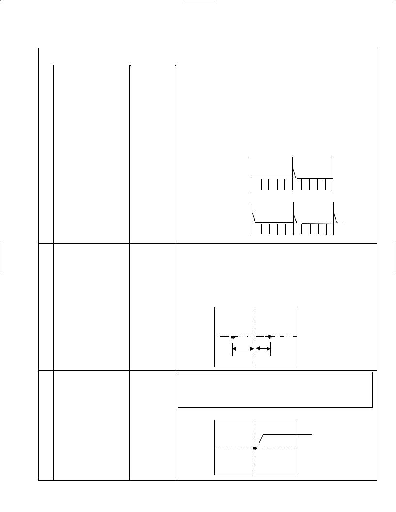
|
|
|
|
|
CS-4125A/CS-4135A |
|||
|
|
|
ADJUSTMENT |
|
|
|
||
|
|
|
|
|
|
|
|
|
|
Item |
Adjustment |
|
|
|
Procedure |
||
|
point |
|
|
|
||||
|
|
|
|
|
|
|
|
|
|
|
|
|
|
|
|
|
|
|
MAG center |
VR303 |
|
|
|
|
|
|
|
|
|
MODE : AUTO |
AC-GND-DC : DC |
|
|
||
|
|
[CS-4125A] |
|
|
|
|||
|
|
|
|
VERT MODE : CH1 |
SWEEP TIME/DIV : 0.1 ms |
|
|
|
|
|
X65-1490 |
|
|
|
|||
|
|
|
|
SOURCE : VERT |
H. VARIABLE : CAL |
|
|
|
|
|
[CS-4135A] |
|
|
|
|||
|
|
|
|
x 10 MAG : ON |
|
|
|
|
|
|
X65-1500 |
|
|
|
|||
1)Input a 0.5 ms marker signal to the CH1 INPUT.
2)Adjust H.POSITION so that the center peak is aligned with the vertical scale center.
3)x 10 MAG switches OFF, and adjust VR303 so that the center
peak of marker signal is aligned with vertical scale center. * Since a gap arises, adjust twice.
26
At the time of x10 MAG ON
At the time of x10 MAG OFF
X. GAIN |
VR151 |
MODE : AUTO |
CH2 AC-GND-DC : AC |
||
|
[CS-4125A] |
||||
|
VERT MODE : CH2 |
CH2 VOLTS/DIV : 10 mV |
|||
|
X65-1490 |
||||
|
SOURCE : VERT |
H. VARIABLE : CAL |
|||
|
[CS-4135A] |
||||
|
X-Y : ON |
|
|
||
|
X65-1500 |
|
|
||
|
|
|
|
|
|
|
|
1) Input a 50 mV square wave signal to the CH2 INPUT. |
|||
|
|
2) VR151 is adjusted so that amplitude may be set to 5 div. |
|||
27 |
|
* Make the adjustment to 5 div., at the CRT center. |
|||
|
|
|
|
|
|
3 div. |
2 div. |
X. POSITION |
VR152 |
|
[CS-4125A] |
|
X65-1490 |
|
[CS-4135A] |
|
X65-1500 |
28
MODE : AUTO |
AC-GND-DC : AC (both CH) |
VERT MODE : CH1 |
V. POSITION : 12 o’clock (both CH) |
SOURCE : VERT |
H. POSITION : 12 o’clock |
X-Y : ON |
|
Adjust VR152 so that spot suits in the horizontal center of a scale.
Adj ust spot to suit the center of a CRT scale.
18
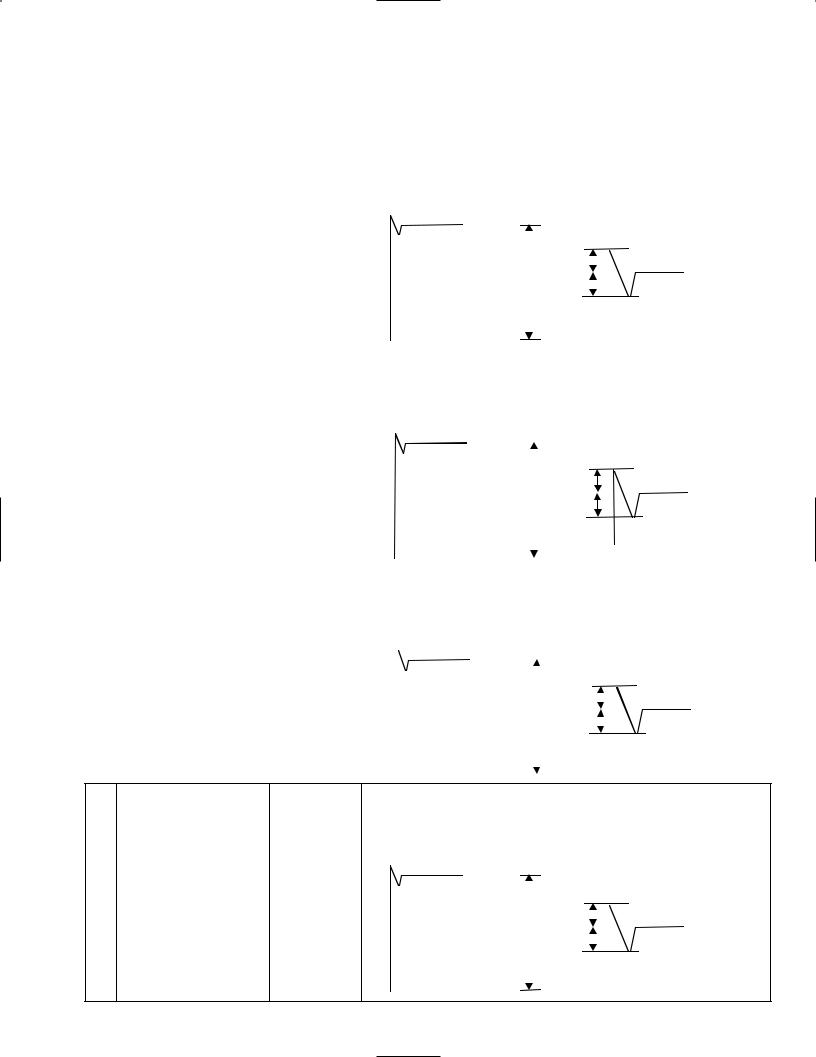
|
|
|
|
|
CS-4125A/CS-4135A |
||||||||||||||||||||||||||||||||
|
|
|
ADJUSTMENT |
|
|
|
|
|
|
|
|||||||||||||||||||||||||||
|
|
|
|
|
|
|
|
|
|
|
|
|
|
|
|
|
|
|
|
|
|
|
|
|
|
|
|
|
|
|
|
|
|
|
|
|
|
|
Item |
Adjustment |
|
|
|
|
|
|
|
|
|
|
|
|
|
Procedure |
|
|
|
|
|
|
|
||||||||||||||
|
point |
|
|
|
|
|
|
|
|
|
|
|
|
|
|
|
|
|
|
|
|
|
|||||||||||||||
|
|
|
|
|
|
|
|
|
|
|
|
|
|
|
|
|
|
|
|
|
|
|
|
|
|
|
|
|
|
|
|
|
|
|
|
|
|
|
|
|
|
|
|
|
|
|
|
|
|
|
|
|
|
|
|
|
|
|
|
|
|
|
|
|
|
|
|
|
|
|
|
|
|
|
|
|
CH2 square wave |
TC56 |
|
|
MODE : AUTO |
|
|
|
|
|
|
AC-GND-DC : DC (both CH) |
|
|
|
|
|
|
|
||||||||||||||||||
|
characteristic |
TC101 |
|
|
|
|
|
|
|
|
|
|
|
|
|
|
|
||||||||||||||||||||
|
|
|
VERT MODE : CH2 |
|
|
|
|
|
|
|
VOLTS/DIV : 10 mV (both CH) |
|
|
|
|
||||||||||||||||||||||
|
[CS-4135A] |
TC 502 |
|
|
|
|
|
|
|
|
|
|
|
|
|
||||||||||||||||||||||
|
|
|
SOURCE : VERT |
|
|
|
|
|
|
|
V. VARIABLE : CAL (both CH) |
|
|
|
|
||||||||||||||||||||||
|
* Use of a 50 Ω |
X65-1500 |
|
|
|
|
|
|
|
|
|
|
|
|
|
||||||||||||||||||||||
|
|
|
|
|
|
|
|
|
|
|
|
|
|
|
|
|
|
|
|
|
|
|
|
|
|
|
|
|
|
|
|
|
|
|
|
||
|
|
|
1) Input a 1 MHz square wave signal to the CH2 INPUT. (5 div. input) |
|
|||||||||||||||||||||||||||||||||
|
terminus machine. |
|
|
|
|
||||||||||||||||||||||||||||||||
|
|
|
|
|
|
|
|
|
|
|
|
|
|
|
|
|
|
|
|
|
|
|
|
|
|
|
|
|
|
|
|
|
|
|
|
|
|
29 |
|
|
|
* |
|
|
|
|
|
|
|
|
|
|
|
|
|
|
|
|
* enlargement |
|
|
|
|
|
|
|
|||||||||
|
|
|
|
|
|
|
|
|
|
|
|
|
|
|
|
|
|
|
|
|
|
|
|
||||||||||||||
|
|
|
|
|
|
|
|
|
|
|
|
|
|
|
|
|
|
|
|
|
|||||||||||||||||
|
|
|
|
|
|
|
|
|
|
|
|
|
|
|
|
|
|
|
|
|
|
|
|
|
|
|
|
|
|
|
|
|
|
|
|
|
|
|
|
|
|
|
|
|
|
|
|
|
|
|
|
|
|
|
|
|
|
|
|
|
|
|
|
|
|
|
|
|
|
|
|
|
|
||
|
|
|
|
|
|
|
|
|
|
5 div. |
|
|
|
|
A |
|
|
|
|
|
|
|
|
|
|
|
|
|
|
||||||||
|
|
|
|
|
|
|
|
|
|
|
|
|
|
|
|
|
|
|
|
|
|
|
|
|
|
|
|
||||||||||
|
|
|
|
|
|
|
|
|
|
|
|
|
|
|
|
|
|
||||||||||||||||||||
|
|
|
|
|
|
|
|
|
|
|
|
|
|
|
|
|
|
|
|
|
|
|
|
|
|
|
|
|
|
||||||||
|
|
|
|
|
|
|
|
|
|
|
|
|
|
|
|
|
|
|
|
|
|
||||||||||||||||
|
|
|
|
|
|
|
|
|
|
|
|
|
|
|
|
|
|
|
|
B |
|
|
|
|
|
|
A |
< |
0.4 |
|
|
||||||
|
|
|
|
|
|
|
|
|
|
|
|
|
|
|
|
|
|
|
|
|
|
|
|
|
|
|
|
|
|
|
|
||||||
|
|
|
|
|
|
|
|
|
|
|
|
|
|
|
|
|
|
|
|
|
|
|
|
|
|
|
|
|
|
= |
|
|
|||||
|
|
|
|
|
|
|
|
|
|
|
|
|
|
|
|
|
|
|
|
|
|
|
|
|
|
|
|
|
|
B |
< |
0.3 |
|
|
|||
|
|
|
|
|
|
|
|
|
|
|
|
|
|
|
|
|
|
|
|
|
|
|
|
|
|
|
|
|
|
= |
|
|
|||||
|
|
|
|
|
|
|
|
|
|
|
|
|
|
|
|
|
|
|
|
|
|
|
|
|
|
|
|
|
|
|
|
|
|
|
< |
|
|
|
|
|
|
|
|
|
|
|
|
|
|
|
|
|
|
|
|
|
|
|
|
|
|
|
|
|
|
|
|
|
|
|
|
|
|
|
|
|
|
|
|
|
|
|
|
|
|
|
|
|
|
|
|
|
|
|
|
|
|
|
|
|
|
|
|
|
|
A + B = 0.6 |
|
||||||
|
|
|
|
|
|
|
|
|
|
|
|
|
|
|
|
|
|
|
|
|
|
|
|
|
|
|
|
|
|||||||||
|
CH1 square wave |
TC6 |
|
|
|
|
|
|
|
|
|
|
|
|
|
|
|
|
|
|
|
|
|
|
|
|
|
|
|
|
|
|
|
|
|
|
|
|
|
|
MODE : AUTO |
|
|
|
|
|
|
|
AC-GND-DC : DC (both CH) |
|
|
|
|
|
|
||||||||||||||||||||
|
characteristic |
TC501 |
|
|
|
|
|
|
|
|
|
|
|
|
|
|
|
||||||||||||||||||||
|
|
|
VERT MODE : CH1 |
|
|
|
|
|
|
|
|
VOLTS/DIV : 10 mV (both CH) |
|
|
|
|
|||||||||||||||||||||
|
[CS-4135A] |
X65-1500 |
|
|
|
|
|
|
|
|
|
|
|
|
|
|
|||||||||||||||||||||
|
|
|
SOURCE : VERT |
|
|
|
|
|
|
|
|
V. VARIABLE : CAL (both CH) |
|
|
|
|
|||||||||||||||||||||
|
* Use of a 50 Ω |
|
|
|
|
|
|
|
|
|
|
|
|
|
|
|
|||||||||||||||||||||
|
|
|
|
|
|
|
|
|
|
|
|
|
|
|
|
|
|
|
|
|
|
|
|
|
|
|
|
|
|
|
|
|
|
|
|
|
|
|
|
|
|
1) Input a 1 MHz square wave signal to the CH1 INPUT. (5 div. input) |
|
||||||||||||||||||||||||||||||||
|
terminus machine. |
|
|
|
|
||||||||||||||||||||||||||||||||
|
|
|
|
|
|
|
|
|
|
|
|
|
|
|
|
|
|
|
|
|
|
|
|
|
|
|
|
|
|
|
|
|
|
|
|
|
|
30 |
|
|
|
* |
|
|
|
|
|
|
|
|
|
|
|
|
|
|
|
|
|
* enlargement |
|
|
|
|
|
|
|
||||||||
|
|
|
|
|
|
|
|
|
|
|
|
|
|
|
|
|
|
|
|
|
|
|
|
|
|
||||||||||||
|
|
|
|
|
|
|
|
|
|
|
|
|
|
|
|
|
|
|
|
|
|
|
|
|
|
||||||||||||
|
|
|
|
|
|
|
|
|
|
|
|
|
|
|
|
|
|
|
|
|
|
|
|
|
|
|
|
|
|
|
|
|
|
|
|
|
|
|
|
|
|
|
|
|
|
|
|
5 div. |
|
|
|
A |
|
|
|
|
|
|
|
||||||||||||||||
|
|
|
|
|
|
|
|
|
|
|
|
|
|
|
|
|
|
|
|
|
|
|
|
|
|
|
|
||||||||||
|
|
|
|
|
|
|
|
|
|
B |
|
< |
|
0.4 |
|
|
|||||||||||||||||||||
|
|
|
|
|
|
|
|
|
|
|
|
|
|
|
|
|
|
|
|
|
|
|
|
||||||||||||||
|
|
|
|
|
|
|
|
|
|
|
|
|
|
|
|
|
|
|
|
|
|
|
|
|
|
|
|
|
|
A |
= |
|
|
|
|||
|
|
|
|
|
|
|
|
|
|
|
|
|
|
|
|
|
|
|
|
|
|
|
|
|
|
|
|
|
|
B |
< |
|
0.3 |
|
|
||
|
|
|
|
|
|
|
|
|
|
|
|
|
|
|
|
|
|
|
|
|
|
|
|
|
|
|
|
|
|
= |
|
|
|
||||
|
|
|
|
|
|
|
|
|
|
|
|
|
|
|
|
|
|
|
|
|
|
|
|
|
|
|
|
|
|
|
|
|
|
|
< |
|
|
|
|
|
|
|
|
|
|
|
|
|
|
|
|
|
|
|
|
|
|
|
|
|
|
|
|
|
|
|
|
A + B = 0.6 |
|
||||||
|
|
|
|
|
|
|
|
|
|
|
|
|
|
|
|
|
|
|
|
|
|
|
|
|
|
|
|
|
|
||||||||
|
|
|
|
|
|
|
|
|
|
|
|
|
|
|
|
|
|
|
|
|
|
|
|
|
|
|
|
|
|
|
|
|
|
|
|
|
|
|
CH2 square wave |
TC56 |
|
|
|
|
|
|
|
|
|
|
|
|
|
|
|
|
|
|
|
|
|
|
|
|
|
|
|
|
|
|
|
|
|
|
|
|
|
|
MODE : AUTO |
|
|
|
|
|
|
AC-GND-DC : DC (both CH) |
|
|
|
|
|
|
|
||||||||||||||||||||
|
characteristic |
TC101 |
|
|
|
|
|
|
|
|
|
|
|
|
|
|
|
||||||||||||||||||||
|
|
|
VERT MODE : CH2 |
|
|
|
|
|
|
|
VOLTS/DIV : 10 mV (both CH) |
|
|
|
|
||||||||||||||||||||||
|
[CS-4125A] |
X65-1490 |
|
|
|
|
|
|
|
|
|
|
|
|
|
||||||||||||||||||||||
|
|
|
SOURCE : VERT |
|
|
|
|
|
|
|
V. VARIABLE : CAL (both CH) |
|
|
|
|
||||||||||||||||||||||
|
* Use of a 50 Ω |
|
|
|
|
|
|
|
|
|
|
|
|
|
|
||||||||||||||||||||||
|
|
|
|
|
|
|
|
|
|
|
|
|
|
|
|
|
|
|
|
|
|
|
|
|
|
|
|
|
|
|
|
|
|
|
|
|
|
|
|
|
|
1) Input a 1 MHz square wave signal to the CH2 INPUT. (5 div. input) |
|
||||||||||||||||||||||||||||||||
|
terminus machine. |
|
|
|
|
||||||||||||||||||||||||||||||||
|
|
|
|
|
|
|
|
|
|
|
|
|
|
|
|
|
|
|
|
|
|
|
|
|
|
|
|
|
|
|
|
|
|
|
|
|
|
31 |
|
|
|
* |
|
|
|
|
|
|
|
|
|
|
|
|
|
|
|
|
|
|
* enlargement |
|
|
|
|
|
|
|
|||||||
|
|
|
|
|
|
|
|
|
|
|
|
|
|
|
|
|
|
|
|
|
|
|
|
|
|
|
|
||||||||||
|
|
|
|
|
|
|
|
|
|
|
|
|
|
|
|
|
|
|
|
|
|
|
|
|
|
|
|
||||||||||
|
|
|
|
|
|
|
|
|
|
|
|
|
|
|
|
|
|
|
|
|
|
|
|
|
|
|
|||||||||||
|
|
|
|
|
|
|
|
|
|
|
|
|
|
|
|
|
|
|
|
|
|
|
|
|
|
|
|
|
|
|
|
|
|
|
|
|
|
|
|
|
|
|
|
|
|
|
|
|
|
|
|
|
|
|
|
|
|
|
|
|
|
|
|
|
|
|
|
|
|||||||
|
|
|
|
|
|
|
|
|
|
5 div. |
|
|
|
A |
|
|
|
|
|
|
|
|
|
|
|
|
|||||||||||
|
|
|
|
|
|
|
|
|
|
|
|
|
|
|
|
|
|
|
|
|
|
|
|||||||||||||||
|
|
|
|
|
|
|
|
|
|
|
|
|
|
|
|
|
|
|
|
|
|||||||||||||||||
|
|
|
|
|
|
|
|
|
|
|
|
|
|
|
|
|
|
|
|
|
|||||||||||||||||
|
|
|
|
|
|
|
|
|
|
|
|
|
|
|
|
|
|
||||||||||||||||||||
|
|
|
|
|
|
|
|
|
|
|
|
|
|
|
|
|
|
|
|
|
B |
|
|
A |
< |
0.2 |
|
|
|||||||||
|
|
|
|
|
|
|
|
|
|
|
|
|
|
|
|
|
|
|
|
|
|
|
|
|
|
|
|
|
|
|
|
||||||
|
|
|
|
|
|
|
|
|
|
|
|
|
|
|
|
|
|
|
|
|
|
|
|
|
|
|
|
|
|
= |
|
|
|||||
|
|
|
|
|
|
|
|
|
|
|
|
|
|
|
|
|
|
|
|
|
|
|
|
|
|
|
|
|
|
B |
< |
0.1 |
|
|
|||
|
|
|
|
|
|
|
|
|
|
|
|
|
|
|
|
|
|
|
|
|
|
|
|
|
|
|
|
|
|
= |
|
|
|||||
|
|
|
|
|
|
|
|
|
|
|
|
|
|
|
|
|
|
|
|
|
|
|
|
|
|
|
|
|
|
|
|
|
|
|
< |
|
|
|
|
|
|
|
|
|
|
|
|
|
|
|
|
|
|
|
|
|
|
|
|
|
|
|
|
|
|
|
|
|
|
|
|
|
|
|
|
|
|
|
|
|
|
|
|
|
|
|
|
|
|
|
|
|
|
|
|
|
|
|
|
|
|
|
|
|
|
A + B = 0.3 |
|
||||||
|
|
|
|
|
|
|
|
|
|
|
|
|
|
|
|
|
|
|
|
|
|
|
|
|
|
|
|
|
|
|
|
|
|
|
|
|
|
CH1 square wave |
TC6 |
characteristic |
X65-1490 |
[CS-4125A] |
|
*Use of a 50 Ω terminus machine.
32
MODE : AUTO |
AC-GND-DC : DC (both CH) |
VERT MODE : CH1 |
VOLTS/DIV : 10 mV (both CH) |
SOURCE : VERT |
V. VARIABLE : CAL (both CH) |
|
|
1) Input a 1 MHz square wave signal to the CH1 INPUT. (5 div. input)
* |
5 div. |
|
A |
* enlargement |
|
|
||||
|
|
|
||||||||
|
|
|
|
|
|
|
||||
|
|
|
|
|
|
|
||||
|
|
|
|
|
|
|
||||
|
|
|
|
|
|
|||||
|
|
|
|
|
|
|
|
|
||
|
|
|
|
B |
|
|
< |
0.2 |
|
|
|
|
|
|
|
|
|||||
|
|
|
|
|
|
|||||
|
|
|
|
|
|
|
|
A = |
|
|
|
|
|
|
|
|
|
< |
0.1 |
|
|
|
|
|
|
|
|
|
|
B = |
|
|
|
|
|
|
|
|
|
|
|
< |
|
|
|
|
|
|
|
|
|
|
|
|
|
|
|
|
|
|
|
|
A + B = |
0.3 |
|
19
Loading...